Design Of Flash Memory Controller
Sanket Jadhav1, Sachin Shinde 2, Mrs. Shruti Oza 3
1&3
Department of Electronics, Bharati Vidyapeeth Deemed University College of engineering, Pune, India
2
PRECISE CONTROLS, MIDC, Satata, India
Abstract— This paper focuses on design of NOR based flash memory controller. Flash memory controller manages data stored in flash memory. There are different commands that to be handled by the controller to operate flash memory. All these signals have been generated through flash memory controller . The results are verified through XILINX ISE simulation tool. Serial communication module is implemented by using Micro-blaze and output is verified on hardware by using LED’s.
Keywords— address and data cycles, commands, command encoding bits, flash memory controller, NOR based flash memory, program address, program data, standard command definitions.
I.INTRODUCTION
There are different types of flash storages available. Depending upon application it is right way to select a flash storage for your application. Basically two types of flash storages are available such as NOR based, NAND based flash memory. There are two types NOR flash memory that is serial NOR and parallel NOR. Also for NAND flash memory serial NAND and parallel NAND flash memories are available.[1]
For reliable code storage such as booting code, application code, operating system NOR based flash storage is preferred. Whereas for NAND flash storage is preferred for high data storage. This paper focuses on implementation of flash memory controller for NOR based flash memory. Flash controller communicates with flash memory to operate flash memory different signals are need to be generated to update the memory contents of flash memory.[4]
Different types of parallel NOR flash memories are available in market. This paper focuses design of flash memory controller for parallel NOR flash memory (M29W128GH). In reference to figure 1, block diagram shows the input and output signals of flash memory. Flash memory controller has to handle all these signals with specified timing parameters to perform operation on flash memory.[4]
The rest of the paper is organised as, section II describes the serial communication module. Control logic is the major part of the flash memory controller which is described in section III. Section IV describes the command decoding formats, algorithms used to implement different blocks which are there in the system. Results are discussed in section V. Section VI concludes the paper.
Fig. 2: Block diagram of Parallel NOR Flash Memory (M29W128GH)
II. SERIAL COMMUNICATION
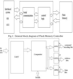
Program address, program data and encoding bits are required by the control logic. As shown in figure 1, these commands or data is sent from an interfaced system or from GUI to the flash memory controller. The communication is serial communication in between GUI and flash memory controller.[2]
Fig.1: General block diagram of Flash Memory Controller
Data from GUI is sent to UART which accepts input serially. Then it is given to the comparator. There is command start bits which are added at the start of each command. Whenever flash memory controller first receiver receive these command start bits it came to know that there is a valid command followed by it. If there no any command start bits at the start of command, then upcoming is discarded because its not an valid command. Since valid command is not received further part of controller is not going to execute. 0xABh are selected as command start bits. For the further operation control logic needs data in parallel form. So three GPIO’s are used to separate the incoming data bits into three parts which are as follows [3]
- Command encoding bits - Program address, - Program data.
Thus, getting these values at the output of serial communication module. Thus serially transmitted data from GUI or from interfaced system is recovered in parallel form in three groups. Command encoding bits are of the size 8 bits, program address is of size 24 bits and program data is of the size of 8 bits.[3]
III. CONTROL LOGIC
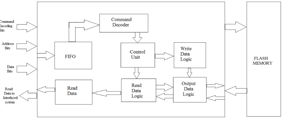
In reference to figure 3, it shows different blocks consists in control logic. It is nothing but the actual part of flash memory controller. All associated are generated at the output of control logic which are required by the flash memory. Function of each block is explained in further part.[3]
A. FIFO:
It stores incoming data bits from the serial communication module. While controller performs program, erase operation memory goes into busy state and controller remains in idle state. At this time incoming commands are need to be stored somewhere, so that incoming commands are not missed.
B. Command Decoder:
It reads commands stored in the FIFO. Command decoder generates commands sequences consisting of address and data cycle which are required by the flash memory. For each command such as PROGRAM command, READ command, ERASE command, there is different command sequence. By using command encoding bits sent from an interfaced system command decoder came to know that which command sequence is to be generated.
C. Control Unit:
It receives address and data cycles from command decoder. There are different states for the controller such as idle state, read state, program state. Whenever controller receives any command there is specified algorithm is executed to execute given command. There are different commands for write data or read data. Accordingly it controls operation of modules such as write data logic module and read data logic module.
D. Write Data Logic and Output Data Logic:
Whenever any command sequence is to be written into command interface of flash memory this block generates required signals such as OE, WE, CE, RST with the help of the block of output data logic. These signals are generated according to timing specifications as mentioned in the data sheet.
E. Read Data Logic and Output Data Logic:
Whenever command is for read data, first of all the command sequence is written into command interface of flash memory. By doing this flash memory goes into read mode. Then read data is available at on the Dout pin of flash memory.
This data is read through output data logic and read data logic and forwarded to interfaced system. Read can be stored in memory if FIFO is used. This FIFO serves as a buffer memory in that case.
IV.IMPLEMENTATION
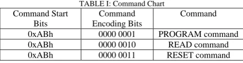
For all the design of flash memory controller Parallel NOR Flash Memory (M29W128GH) is considered in x8 bit mode and its required standard command definitions are mentioned in TABLE II. In reference to table I, it shows the encoding bits used for different commands. 0xABh is the start bit for each command. Start bits are added to each command while sending command from interfaced system. Start bits denotes valid command transmission. If any command is received at the controller without command start bits, then that frame is discarded by the controller. [5]
TABLE I: Command Chart
Command Start Bits
Command Encoding Bits
Command
0xABh 0000 0001 PROGRAM command 0xABh 0000 0010 READ command
0xABh 0000 0011 RESET command
In reference to figure 4, shows the frame format for each command. First field consists of start bits, second field consists of command encoding bits, third fields consist of address bits and forth field consists of data bits.
Command Start Bits Command Encoding Bits Address Bits Data Bits
Fig.4: Frame Format Sent Through Interfaced System
In reference to TABLE II, there are address and data cycles for each command. These address and data cycles, other associated signals are generated at the output of controller. Which address – data cycles are generated for which commands is specified in data sheets. According to which these address – data cycles need to be generated, then and then only flash memory goes into desired mode otherwise not.[5]
TABLE II: Standard Command Definition – Address Data Cycles
Designing of each block which is there in control logic requires implementation of different algorithms to achieve desired output. For each block there is an enable or disable pin which is driven by its previous block from which it gets input. For example when valid command is received in FIFO, to enable command decoder one pin is used named cmnd_start. This goes high after valid reception of command and read operation from FIFO. After decoding of input command decoder generates address – data cycles at its output. With this output it sends enable signal to turn on the control fsm block to perform further operation. Until it gets enable signal controller remains in idle state.[5] While developing algorithms for commands specifications mentioned in data sheet are to be considered for implementation. [6]
A. PROGRAM Command:
It is used to program a value to one address in the memory array. It requires four write operations then flash memory goes into this mode. Fourth write operation latches program address (PA) and program data (PD). Programming operation can be suspended by the PROGRAM SUSPEND command. Then to resume the suspended operation PROGRAM RESUM command is used. After successfully completion of PROGRAM operation device i.e. flash memory returns to read mode.[5]
B. READ Command:
F0h command returns the device to read mode. It requires two bus write operation. In the second cycle read address (RA) is applied to the flash memory. After getting this read address, data from that address is available on DQ pins of flash memory. By using output data logic and read data logic this data is read and forwarded to interfaced system.[5]
C. RESET Command:
Three bus WRITE operations can be used to issue the RESET command. Address – data cycles for this RESET commands are shown in TABLE II. After RESET operation device goes into READ mode. If RESET command is issued during timeout of BLOCK EARSE command it requires 10 µs to abort. During this no valid data can be read.[5]
V. RESULT
For flash memory controller, Output of serial communication module is verified on the hardware by using bank of LED’s. Code is burned into FPGA. Commands are sent from hyper terminal of PC. Data is sent serially through hyper terminal. Serial communication module checks whether valid command received or not. After reception of valid command, Command encoding bits, address bits, data bits are available at the output. For invalid command none of these bits are available at the output.
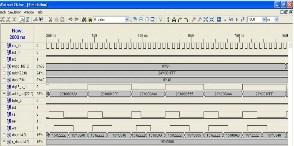
In reference to figure 5, for verification “AB01001FFF40” is sent through hyper terminal.
Where,
ABh = command start bits 01h = command encoding bits 001FFFh = address bits
40h = data bits
Since it is valid command all bits are available at the output of serial communication module. Out of these command start bits and data bits are verified on hardware by using LEDs.
Fig. 5: Command sent through Hyper Terminal of PC
Command A1 D1 A2 D2 A3 D3 A4
D4 PROGRAM
command AAA AA 555 55 AAA A0 A PD READ
command X F0 RA - - - - -
RESET
In reference to figure 6, on the left sided 8 LEDs received command encoding bits (01h) i.e. “0000 0001”. Data bits are received right sided LEDs. Received data bits are (40h) i.e. “0100 0000”.
Fig.6: Encoding bits and data bits received at the output of Serial Communication module
In reference to figure 7, for verification “0A02001FFFAD” is sent through hyper terminal.
Where,
0Ah = command start bits 02h = command encoding bits 001FFFh = address bits
ADh = data bits
Fig. 7: Command sent through Hyper Terminal of PC
Since valid command start bits are not there at the start command, serial communication module is not going give
any output to the control logic module. So, control logic remains in idle state
In reference to figure 8, due invalid command output all LED’s are off.
Fig. 8: No any Output at the output of serial communication module
Fig. 9: RTL Schematic for the Control Unit Module
Fig.11: Signals Generated by the Control unit for READ Command
In reference to figure 9, it shows RTL schematic which is generated for the control unit module. All blocks which are shown in figure 3 are implemented using VHDL. In reference to figure 10 and figure 11, command encoding bits, address bits are and data bits are applied to it. These bits are received from serial communication module only when valid command is received at its input.On the basis of these inputs bits control units generates necessary signals and address – data cycles for the flash memory.
VI. CONCLUSION
When any command is sent through interfaced system the serial communication block check for the valid reception of a command. If valid command is received , it converts incoming bit stream into three parts which are reqquired by the control logic module. After reception of valid command it is first of all saved into FIFO. Then command decoder checks whether there is any command for execution.If any command is present for the execution , it read this command from FIFO and generate necessary address-data cycles. Further reqired signals such as OE, WE,CE etc signals are generated with their timing parameters by using address-data cycles. Thus controller execute command received by it. This paper focuses on implementation of PROGRAM command, READ
command, RESET command for the flash memory controller. For the implementation of serial communication module Microblaze is used. Code for the control unit model is implemented in VHDL language and XILINX simulation tool is used to simulate the design and generate the waveforms.
REFERENCES
[1] Parallel flash memory information http://www.micron .com/products/nor-flash.
[2] Microblaze processor reference guide_pdf http:// www. xilinx.com/support/ Documentation /sw / mb_ref _ guide .pdf [3] Microblaze tutorial implementation http:// www.
smdp2vlsi.gov.in/ smdp2vlsi/ downloads/mb_tutorial.pdf [4] NOR/NAND Flash Guide_pdf http://www. Micron
.com/products/nor-flash/ parallel-nor-flash/Download - guide. [5] Parallel NOR Flash Embedded MemoryM29W128,
M29W128GL -datasheet http://www.micron.com/ Parts/nor-flash/parallel-nor-flash/m29w128gh70n6e
[6] Hoeseun Jung, Sanghyuk Jung, Yong Song “Architecture Exploration of Flash Memory Storage Controller Through a Cycle Accurate Profiling ”Proc. IEEE Transactions on Consumer Electronics,Vol. 57, No. 4, ovember 2011.