Implementation of DRAM Cell Using
Transmission Gate
Pranita J. Giri1, Sunanda K. Kapde2
PG Student, Department of E&TC, Deogiri Institute of Engineering & Management Studies, Aurangabad (MS), India1
Assistant Professor, Department of E&TC, Deogiri Institute of Engineering & Management Studies, Aurangabad
(MS), India2
ABSTRACT: Dynamic random access memory plays very important role in the world of microprocessor. DRAM offers very high density & low cost, due to this DRAM is used by advanced processors for on chip data & program memory. In today’s generation trade off is in low power consumption, low leakage current, low cost & compactness, but design complexity is increased due to reduction in size. Leakage power and delay are most important factors which affects the performance of DRAM cell. In this paper the analysis of DRAM cell by using transmission gate has been shown. In proposed circuit transmission gate is used as access transistor. This circuit offers improved process variation and improved read stability which makes it a promising choice for on chip memory for next generation microprocessor.
KEYWORDS:DRAM, transistor, Leakage power and delay.
I. INTRODUCTION
Memories play an essential role in design of any electronics design; there are two types of memories used in modern day i.e. ROM and RAM (Read Only Memory and Random Access Memory). Again RAM is of two types Dynamic Random Access Memory (DRAM) and Static Random Access Memory (SRAM) [4]. In new generation microprocessors, on chip memories provides high system performance utilizing a significant portion of entire die space. On chip caches based on SRAM cells which are scaled down very well with technology as technology nano-scaling promises increasing transistor density & increasing performance in microprocessors. However, stability, performance & leakage power are major issues in scaling process of SRAM cell; we can avoid scaling limitations of SRAM cell by designing a new circuit.
Dynamic memories give better solution, as it provides good data storage structure in the process core. DRAM is volatile memory, which holds instructions temporarily required by CPU for performing the task. DRAM cell is constructed by using transistor and capacitor, where capacitor is used to produce 1 or 0. As capacitor is used in DRAM cell, information stored in capacitor degraded constantly, because of this DRAM cell need to be refreshed periodically which leads to the power consumption. The design of conventional 3T DRAM cell decreases the power consumption and access delay but it doesn’t provide good stability. We proposed a DRAM cell using transmission gate to improve the stability and compare their performance with 3T DRAM cell.
The rest of this paper organized as: in Section II we discuss the different systems, Section III describes structure of DRAM cell using Transmission gate, and in section IV simulation results are given. Conclusion is presented in section V.
II. LITERATURE SURVEY
ISSN(Online): 2319-8753 ISSN (Print): 2347-6710
I
nternational
J
ournal of
I
nnovative
R
esearch in
S
cience,
E
ngineering and
T
echnology
(An ISO 3297: 2007 Certified Organization)
Website: www.ijirset.com
Vol. 6, Issue 4, April 2017
described. Fig. 1 shows the structure of 3T DRAM cell, here three transistors and one capacitor is used. Transistor M2 is used as access transistor to store information data. Transistor M1 and M3 are used as switches, each switch is turn ON or OFF according to write and read operation respectively
Fig. 1 shows the structure of 3T DRAM cell [1].
Laxmi singh and Ajay Somkuwar [2], presents Dynamic Random Access Memory with Self-controllable Voltage Level to reduce low leakage current in VLSI. This research paper implements the 3T DRAM with Self-controllable Voltage Level technique. In this system three NMOS M1, M2 and M3 are used. M1 and M3 are the access transistor and by using these read and write operation can be controlled. At the time of write operation M1 is on and M3 is off (the data is stored by charging the capacitor) and for the read operation M1 is off and M3 is on. This system used self controllable voltage level to implement the 3T DRAM. Table 1 shows the simulation of 3T DRAM with self controllable voltage level.
Table 1 Simulation result of SVL based 3T DRAM
Circuit Leakage current
3T dram during write operation 0.164ma
3T DRAM with SVL 0.071ma
This system presented a 3T DRAM with self controllable voltage level. To implement 3T DRAM with self controllable voltage level gives the advantageous of reduction up to 57%.
Fig. 2 TG-based fully 8T SRAM cell (TG8T) [3].
TG8T SRAM consist two operation read and write, at the time of write operation both the line are at opposite voltages in which BL is at high then BLB is at low, at the time of read operation both the lines are at high voltage and WL is raised at high voltage WLB at 0. This system improved leakage current of TG8T SRAM cell as compared to Conventional 6T SRAM, shown in table 2.
Table 2. Comparison of parameter of TG8T SRAM cell with 6T SRAM [3].
Parameter Conventional 6T SRAM
Transmission gate 8T SRAM (TG8T)
Write Write
Leakage current 69.22*10-12A 229.2*10-15 A
Leakage power 7.346nW 2.97 nW
Delay 20.57 ns 20.92 ns
SNR 1.58dB 4.77dB
III.PROPOSED SYSTEM
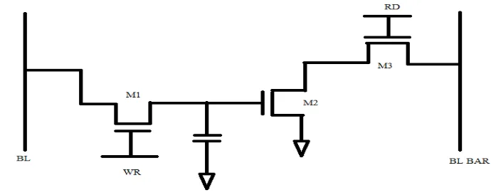
This section describes the proposed structure of DRAM cell using transmission gate. The main objective behind design of this cell is to provide write stability & to improve the performance. Fig 3 shows the schematic of DRAM cell using transmission gate. Here transmission gate is used as switch.
ISSN(Online): 2319-8753 ISSN (Print): 2347-6710
I
nternational
J
ournal of
I
nnovative
R
esearch in
S
cience,
E
ngineering and
T
echnology
(An ISO 3297: 2007 Certified Organization)
Website: www.ijirset.com
Vol. 6, Issue 4, April 2017
There are basically two operations i.e. read and write operation. During write operation, both the bit lines are at opposite voltages, that means if bit line BL is at high voltage then BLB at low voltage and vice versa. When WR becomes high and WRN becomes low this enables transmission gate and the charge on BL is stored in capacitor and data writes on output port Q. During read operation the RD should be high; this enables the transistor M3, both bit line behaves as output, one of bit line starts discharging and that instant data is going to be read.
IV.SIMULATIONRESULTS
The main objective of this work is to improve read stability of memory cell and to meet all challenges in designing of memory cell at nanoscale technology. All simulation have been performed on Tanner EDA tool version 13.0 using 22nm technology with input ranging from 0.4v to 1v.
A. POWER CONSUMPTION
Whenever the PMOS and NMOS transistors are in OFF state, the CMOS inverter is in stable state. No current flows through the power supply to ground. However, small amount of current flow through the OFF state transistor and it gives rise to, leakage power consumption, as shown in equation 1.
P=IL × VDD
Sr. No. Applied Voltage Power Consumption Discharge of Capacitance
1 0.4v 438.94pf 24.26mv
2 0.6v 340.07pf 20mv
3 0.8v 290.24pf 10mv
4 1v 128.65pf 10mv
B. READ STABILITY
Proposed system provides improved read stability. Fig. 3 and Fig. 4 shows the response of proposed system and existing system during read operation. In figure, Q indicates stored value and RBL indicates output value. Fig. 3 shows that stored value and outputted value is logic 1. Fig. 4 shows that stored value is logic 1, but outputted value is logic 0. This shows that proposed system provides read stability as compare to existing system.
Fig.5 Read 1 of Existing System
V. CONCLUSION
We have proposed a DRAM cell using transmission gate in which we present read/write operation at a range of operating supply voltage. In this paper it is observed that by using transmission gate instead of NMOS transistor in the circuit we can improve the read operation and also it has been observed that power consumption is decreased with increase in voltage. It can be considered that high performance and a lesser amount of power consumption as increase in working voltage at 22 nanometer technology in Tanner EDA tool.
REFERENCES
[1] Priyanka Kushwah, Nikhil Saxena, Shyam Akashe and Saurabh Khandelwal, “Reduction of Leakage Power & Noise for DRAM Design using Sleep Transistor Technique”, 2015 Fifth International Conference on Advanced Computing & Communication Technologies, pp. 80-83. [2] Laxmi singh and Ajay Somkuwar, “Dynamic Random Access Memory with Self-controllable Voltage Level to reduce low leakage current in
VLSI”, International Journal of Engineering Research and Applications (IJERA), Vol. 3, Issue 1, January -February 2013, pp.1893-1897. [3] Joshika Sharma, Prof. Saurabh Khandelwal and Prof. Shyam Akashe, “Implementation of high performance SRAM Cell Using Transmission
Gate” , Fifth International Conference on Advanced Computing & Communication Technologies, 201, pp. 257-260.
![Fig. 2 TG-based fully 8T SRAM cell (TG8T) [3].](https://thumb-us.123doks.com/thumbv2/123dok_us/1611387.1199706/3.595.128.442.600.755/fig-tg-based-fully-t-sram-cell-tg.webp)
