Chapter 11
The I
2
C Protocol
• Developed by Philips in late 1980s
• Version 1.0 published in 1992
– Supports standard (100 Kbps) and fast (400 Kbps) mode
• Version 2.0 published in 1998
– High-speed mode (3.4 Mbps) added
• Classifies devices into slave and master
• Allows multiple masters to be attached to the same bus
• The master device uses either a 7-bit or 10-bit address to specify
the slave device as its partner of data communication.
• Supports bi-directional data transfer
I
2
C Signal Level
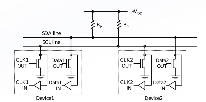
• Float high and driven low
• Use the SCL signal to carry clock signal to synchronize
data transfer
• Use the SDA signal to carry data and address
• The SDA and SCL pins of I
2C devices (masters and
slaves) are open-drain and need external pull up
resistors.
• The resistors 2.2 K
and 1 K
are recommended for
+VDD
RP RP
CLK1 OUT
CLK1 IN
Data1 OUT
Data1 IN
CLK2 OUT
CLK2 IN
Data2 OUT
Data2 IN
Device 1 Device 2
SDA line SCL line
Signal Components
• I
2C data transfer consists of 5 signal
components:
– Start (S)
– Stop (P)
– Repeated Start (R)
– Data
SDA
SCL
Figure 11.2 I2C Start condition
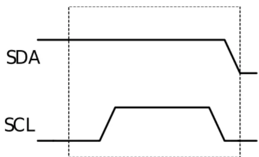
Start Condition
• Used to indicate that a device would like to
transfer data on the I
2C bus
• Represented by the SDA line going low when
the clock (SCL) signal is high
SDA
SCL
Figure 11.3 Stop (P) condition
Stop Condition
• A condition that a device wants to release the I
2C bus
• Is represented by the SDA signal going high when the
SCL signal is high
• Once the stop condition is complete, both the SCL and
SDA
SCL
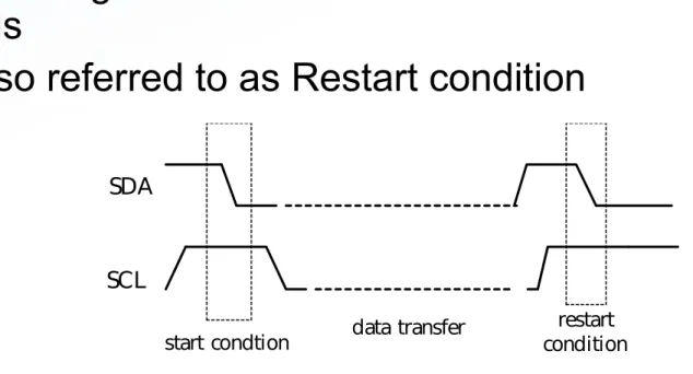
Figure 11.4 Restart condition
start condtion data transfer conditionrestart
Repeated Start (R) Condition
• A Start signal generated without first generating a Stop
condition to terminate the communication
• Used by the master to communicate with another slave
or change data transfer direction without releasing the
bus
SDA
SCL
Figure 11.5 I2C bus data elements
Note. Data bit is always stable when clock (SCL) is high
Data
• It represents the transfer of eight bits of information.
• Data on the SDA line is considered valid only when the SCL signal
is high.
SDA
SCL
Figure 11.6 ACK condition
SDA
SCL
Figure 11.7 NACK condition
Acknowledge (ACK) Condition
• Data transfer needs to be acknowledged either positively (A) or
negatively (NACK).
• A device acknowledges a byte it receives positively by bringing the
SDA line low during the ninth clock pulse of SCL.
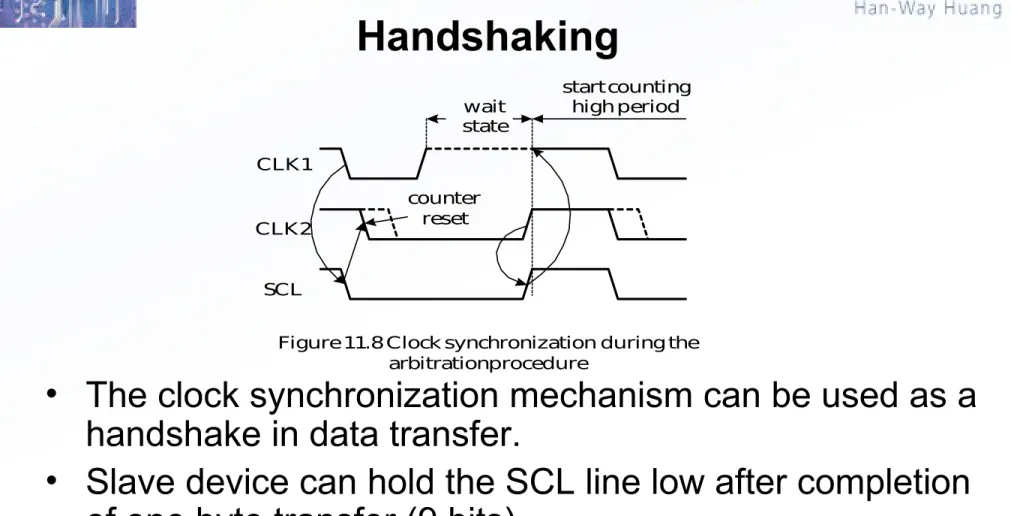
Synchronization
(1 of 2)
• All masters generate their clocks on the SCL line to transfer
messages on the I2C bus.
• A defined clock is needed for the bit-by-bit arbitration procedure to
take place.
• Most microcontrollers generate the SCL clock by counting down a
programmable reload value using the instruction clock signal.
• Clock synchronization occurs when multiple masters attempt to
drive the I2C bus and before the arbitration scheme can decide
which master is the winner.
• Clock synchronization is performed using the wired-AND connection
of I2C interfaces to the SCL line.
Synchronization
(2 of 2)
• A master device that is counting off their low period will hold the
SCL line low until the counter is count down to 0. At this point, the
device will release the SCL line to high.
• If there are other devices holding the SCL low, then the SCL line will
remain low until all master devices have counted down to 0. At this
point, the SCL line will go high and all devices will start to count
high.
• The SCL line will be held low by the device with the longest low
period.
wait state
start counting high period
counter reset CLK1
CLK2
SCL
Figure 11.8 Clock synchronization during the arbitration procedure
Handshaking
• The clock synchronization mechanism can be used as a
handshake in data transfer.
• Slave device can hold the SCL line low after completion
of one byte transfer (9 bits).
master 1 loses arbitration Data 1 SDA
SCL
Data1
Data2
SDA
Figure 11.9 A rbitration procedure of two masters
Arbitration
•
In the event two or more master devices attempt to begin a transfer at the
same time, an arbitration scheme is employed to force one or more masters
to give up the bus.
•
The master devices continue to transmit data until one master attempts to
send a high while the other transmits a low.
•
Since the SDA bus has open drain, the master device that attempts to send
a high will detect a low. At this point, it will stop driving the bus.
A6 A5 A4 A3 A2 A1 A0 R/W
Figure 11.13a 7-bit I2C address
1 1 1 1 0 A9 A8 R/W A7 A6 A5 A4 A3 A2 A1 A0
Figure 11.13b 10-bit I2C address
I
2
C Addressing Methods
• I
2C protocol allows master devices to use either the 7-bit and 10-bit
address to specify the slave device for data communication.
• The 7-bit addressing uses the upper 7 bits of the address byte for
address and the least significant bit to specify the data transfer
direction. The format is shown in Figure 11.13.
• The 10-bit addressing uses two bytes to carry the address
information.
– The bit 0 of the high byte is used to indicate the data transfer direction.
– The upper 7 bits have the pattern of 1111 0xx with xx representing the
S Slave address R/ W A Data A Data A/ A P
data transferred (n bytes + acknowledge) '0' (write)
from master to slave
from slave to master
A = acknowledge (SDA low) A = not acknowledge (SDA high) S = start condition
P = stop condition
Figure 11.10 A master-transmitter addressing a slave receiver with a 7-bit address. The transfer direction is not changed.
Data Transfer Format (7-bit Addressing)
(1 of 2)
• Master transmitter to slave receiver – shown in Figure 11.10
• Master reads slave immediately after the first byte (address byte) –
shown in Figure 11.11
S Slave address R/ W A Data Data P
data transferred (n bytes + acknowledge) '1' (read)
Figure 11.11 A master reads a slave immediately after the first byte A A
S Slave address R/ W A Data Data
read or write
Figure 11.12 Combined format
A/ A R Slave address R/ W A/ A P (n bytes +
ack.) repeated start read or write A
(n bytes + ack.)* direction of transfer may change at this point
* not shaded because transfer direction of data and acknowledge bits depends on R/ W bits
S slave address
1st 7 bits R/ W A1
slave address
2nd byte A2 data A data A/ A P
(write)
Figure 11.16 A master-transmitter addresses a slave-receiver with a 10-bit address 11110XX 0
Data Transfer Format—10-bit Addressing (1 of 3)
•
Master transmitter transmits to slave receiver with a 10-bit address –Figure
11.16
•
Master receiver reads slave transmitter with a 10-bit address –Figure 11.17
•
Restart condition generated in this format
•
Combined format – A master sends data to a slave and then reads data
from the same slave. Shown in Figure 11.18.
•
Combined format – A master sends data to one slave and then transmit
data to another slave. Shown in Figure 11.19.
S slave address
1st 7 bits R/ W A1
slave address
2nd byte A2 R data data P
(write)
Figure 11.17 A master-receiver addresses a slave-transmitter with a 10-bit address slave address
1st 7 bits R/ W A3 A A 11110XX 0 11110XX 1
(read)
S slave address
1st 7 bits R/ W A
slave address
2nd byte A data A data A/ A
P (write)
Figure 11.18 Combined format. A master addresses a slave with a 10-bit address, then transmit data to this slave and reads data from this slave.
R slave address
1st 7 bits R/ W A data A data A 11110XX 0
11110XX 1
(read)
Figure 11.19 Combined format. A master transmits data to two slaves, both with 10-bit addresses.
S slave address
1st 7 bits R/ W A
slave address
2nd byte A data A data A/ A
P (write)
R slave address
1st 7 bits R/ W A data A data A/ A
11110XX 0
11110XX 0
(write)
slave address 2nd byte A
S 7-bit slave
address R/ W A data A data A/ A
P (write)
Figure 11.20 Combined format. A master transmits data to two slaves, one with 7-bit address, and one with 10-bit address.
R 1st 7 bits of 10-bitslave address R/ W A data A data A/ A 0
11110XX 0
(write)
2nd byte of 10-bit slave address A
Overview of the HCS12 I
2C Module
•
Implements a subset of the I2C protocol
•
Provides interrupts on start and stop bits in hardware to determine if the I
2C
bus is free
•
Supports only 7-bit addressing
•
Supports 100 Kbps baud rate but requires the user to limit the slow rate to no
higher than 100 ns if the 400 Kbps baud is to be used
•
Limit the maximum bus capacitance to 400 pF for all conditions.
•
Use PJ7 (SCL) and PJ6 (SDA) pins to support the I
2C communication.
•
Use five registers to support its operation:
– I2C Control Register (IBCR)
– I2C status Register (IBSR)
– I2C data I/O register (IBDR)
– I2C Frequency Divider Register (IBFD)
ADDR_DECODE
CTRL_REG FREQ_REG ADDR_REG STATUS_REG DATA_REG DATA_MUX
input sync
In/ Out data shift register Start/ stop
arbitration control clock
control
address compare
SCL SDA
Address I
2C
interrupt data bus
ADR7 ADR6 ADR5 ADR4 ADR3 ADR2 ADR1 0 0 1
2 3
4 5
6 7
Figure 11.22 I2C address register (IBAD)
Registers for I
2
C Operation
• I
2C Address Register (IBAD)
– Contains an address to which it will respond when the
I
2
C Data Register (IBDR)
• In master transmit mode, a data transfer is
started whenever this register is written into.
• The most significant bit is shifted out first.
IBEN IBIE MS/ SL Tx/ Rx TxAK RSTA 0 IBSWAI 0 1 2 3 4 5 6 7
Figure 11.23 I2C control register (IBCR)
reset: 0 0 0 0 0 0 0 0
IBEN: I2C bus enable
0 = I2C module is reset and disabled
1 = I2C module is enabled. This bit must be set before any other IBCR bits have
any effect.
IBIE: I2C bus interrupt enable
0 = interrupts from the I2C module are disabled.
1 = interrupts from the I2C module enabled
MS/ SL: master/ slave mode select 0 = slave mode
1 = master mode
Tx/ Rx: Transmit/ Receive mode select 0 = receive
1 = transmit
TXAK: Transmit acknowledge
0 = An acknowledge signal will be sent out to the I2C bus on the 9th clock bit
after receiving one byte of data
1 = No acknowledge signal response is sent RSTA: Repeat start
0 = no action
1 = generate a repeat start cycle IBSWAI: I2C bus stop in wait mode
0 = I2C module clock operates normally
1 = stop generating I2C module clock in wait mode
The I
2
C Control Register
(2 of 2)
• When setting the MS/SL bit from 0 to1, a start signal is
generated on the I
2C bus and the master mode is
selected.
• In the master mode, the Tx/Rx bit should be set
according to the type of transfer required.
• The TxAK bit specifies the value driven onto the SDA line
during data acknowledge cycles for both master and
slave receivers.
• I
2C module always acknowledges the address matches
regardless of the value of TxAK.
The I
2
C Status Register (IBSR)
(1 of 2)
• When a byte is being transferred, the TCF bit is
cleared.
• When the I
2C is configured as a slave and the
address matches, then the IAAS bit will be set.
• The IBIF bit will be set under three
circumstances:
– Arbitration lost (IBAL bit is set)
TCF IAAS IBB IBAL 0 SRW IBIF RXAK 0 1 2 3 4 5 6 7
Figure 11.24 I2C status register (IBSR)
reset: 1 0 0 0 0 0 0 0
TCF: Data transferring bit 0 = I2C transfer in progress
1 = I2C transfer complete
IAAS: Addressed as a slave 0 = not addressed
1 = addressed as a slave IBB: Bus busy bit
0 = the bus enters idle state 1 = I2C bus is busy
IBAL: Arbitration lost 0 = arbitration is not lost 1 = arbitration is lost SRW: Slave read/ write
0 = slave receive, master writing to slave 1 = slave transmit, master reading from slave IBIF: I2C bus interrupt
0 = no bus interrupt 1 = bus interrupt
RXAK: Receive acknowledge
This bit reflects the value of SDA during the acknowledge bit of a cycle. 0 = acknowledge received
1 = no acknowledge received
SCL divider
SDA hold SCL
SDA
SCL hold (start) SCL hold(stop)
start
condition conditionstop SCL
SDA
Figure 11.25 SCL divider and SDA hold
Table 11.2 I2C bus timing requirements
symbol
SCL clock frequency SCL hold (start) SCL hold (stop) SDA hold fSCL
tHD;STA tSU;STO tHD;DAT
parameter standard mode fast mode min. max. min. max.
0 4.0 4.0 0 100 -3.45 0 0.6 0.6 0 400 -0.9 unit KHz s s s
I
2
C Frequency Divider Register (IBFD)
• Four timing
requirements to
be met:
– SCL divider
– SDA hold time
– SCL hold time for
start condition
IBC7 IBC6 IBC5 IBC4 IBC3 IBC2 IBC1 IBC0 0 1 2 3 4 5 6 7
Figure 11.26 I2C frequency divider register (IBFD)
Table 11.3 Multiply factor
IBC7~IBC6 Multiply factor 00 01 10 11 01 02 04 reserved
Table 11.4 Prescaler divider IBC5~IBC3 000 001 010 011 100 101 110 111 scl2start (clocks) 2 2 2 6 14 30 62 126 scl2stop (clocks) 7 7 9 9 17 33 65 129 scl2tap (clocks) 4 4 6 6 14 30 62 126 tap2tap (clocks) 1 2 4 8 16 32 64 128
The Use of the IBFD Register (1 of 2)
• IBC7-IBC6: multiply factor (shown in Table 11.3)
• IBC5-IBC3: prescaler divider (shown in Table 11.4)
Table 11.5 I2C bus tap and prescale values IBC2~IBC0 000 001 010 011 100 101 110 111 SCL tap (clocks) 5 6 7 8 9 10 12 15 SDA tap (clocks) 1 1 2 2 3 3 4 4
The Use of the IBFD Register
(2 of 2)
•
Using Table 11.3, 11.4, and 11.5 is a laborious process.
•
These three tables can be combined into the Table 11.6.
– With Table 11.6, finding values to be written into the IBFD register becomes a simple table look up.
•
By
dividing
the intended
baud rate
into the
bus clock
, one can locate one
or multiple rows in Table 11.6 with the same SCL divider value.
• Example 11.1 Assuming that the HCS12 is running with a 24 MHz bus clock,
compute the values to be written into the IBFD register to set the baud rate to 100 KHz and 400 KHz.
• Solution:
• Case 1: baud rate = 100 KHz
SCL divider = 24 MHz 100KHz = 240 From Table 11.6,
SDA hold time = 33 E clock cycles = 1.375 ms < 3.45 ms
SCL hold time (start) = 118 E clock cycles = 4.92 ms > 4.0 ms SCL hold time (stop) = 121 E clock cycles = 5.04 ms > 4.0 ms The computed value satisfies the timing requirement.
Write the value $1F into the IBFD register at 100 KHz baud rate.
• Case 2: baud rate = 400 KHz
SCL divider = 24 MHz 400KHz = 60
From Table 11.6, the corresponding IBC value is $45.
SDA hold time = 18 E clock cycles = 0.75 ms < 0.9 ms
SCL hold time (start) = 22 E clock cycles = 0.917 ms > 0.6 ms SCL hold time (stop) = 121 E clock cycles = 1.33 ms > 0.6 ms The computed value satisfies the timing requirement.
; parameters are passed in accumulator A (baud rate) and B (slave address)
openI2C bset IBCR,IBEN ; enable I2C module
staa IBFD ; establish SCL frequency
stab IBAD ; establish I2C module slave address bclr IBCR,IBIE ; disable I2C interrupt
bset IBCR,IBSWAI ; disable I2C in wait mode rts
void openI2C (char ibc, char i2c_ID) {
IBCR |= IBEN; /* enable I2C module */ IBFD = ibc; /* set up I2C baud rate */ IBAD = i2c_ID; /* set up slave address */ IBCR &= ~IBIE; /* disable I2C interrupt */ IBCR |= IBSWAI; /* disable I2C in wait mode */ }
Configuring the I
2C Module
•
Compute an appropriate value and write it into the IBFD register.
•
Load a value into the IBAD register if the MCU may operate in slave mode.
•
Set the IBEN bit of the IBCR register to enable I
2C module.
sendSlaveID brset IBSR,IBB,* ; wait until I2C bus is free
bset IBCR,TXRX+MSSL ; generate a start condition staa IBDR ; send out the slave address
brclr IBSR,IBIF,* ; wait for address transmission to complete movb #IBIF,IBSR ; clear the IBIF flag
rts
void sendSlaveID (char cx) {
while (IBSR&IBB); /* wait until I2C bus is idle */
IBCR |= TXRX+MSSL; /* generate a start condition */
IBDR = cx; /* send out the slave address with R/W bit set to 1*/ while(!(IBSR & IBIF)); /* wait for address transmission to complete */
IBSR = IBIF; /* clear IBIF flag */ }
Programming the I
2
C Module
• Instruction sequence to send a byte in accumulator A
staa IBDR
brclr IBSR,IBIF,* ; wait until IBIF flag is set to 1 movb #IBIF,IBSR ; clear the IBIF flag
• C statements to send a byte to I
2C bus
IBDR = cx; /* send out the value cx */
while (!(IBSR & IBIF)); /* wait until the byte is shifted out */ IBSR = IBIF; /* clear the IBIF flag */
• Instruction sequence to read a byte and acknowledge it
bclr IBCR,TXRX+TXAK ; prepare to receive and acknowledge ldaa IBDR ; a dummy read to trigger 9 clock pulses brclr IBSR,IBIF,* ; wait until the data byte is shifted in
movb #IBIF,IBSR ; clear the IBIF flag
• C Statements to read a byte from the I
2C bus
IBCR &= ~(TXRX + TXAK); /* prepare to receive and acknowledge */ dummy = IBDR; /* a dummy read */
while(!(IBSR & IBIF)); /* wait for the byte to shift in */ IBSR = IBIF; /* clear the IBIF flag */
buf = IBDR; /* place the received byte in buf and also initiate the next read sequence */
• Instruction Sequence to Read a Byte, Send NACK, and Generate Stop Condition
bclr IBCR,TXRX ; prepare to receive
bset IBCR,TXAK ; to send negative acknowledgement ldaa IBDR ; dummy read to trigger clock pulses brclr IBSR,IBIF,* ; wait until the byte is shifted in
movb #IBIF,IBSR ; clear the IBIF flag
• C statements to Read a Byte, send NACK, and generate a Stop condition
IBCR &= ~TXRX; /* prepare to receive */
IBCR |= TXAK; /* prepare not to acknowledge */
dummy = IBDR; /* a dummy read to trigger 9 clock pulses */ while(!(IBSR & IBIF)); /* wait for a byte to shift in */
IBSR = IBIF; /* clear the IBIF flag */
I
2
C Data Transfer in Slave Mode
• After reset and stop condition, the I
2C module is in slave mode.
• Once in slave mode, the I
2C module waits for a start condition to
come.
• Following the start condition, eight bits are shifted into the IBAD
register.
• The value of the upper 7 bits of the received byte is compared with
the IBAD register.
• If the address matches, the following events occur:
– The bit 0 of the address byte is copied into the SRW bit of the IBSR
register.
– The IAAS bit is set to indicate the address match.
brset IBSR,IAAS,addr_match ; is address matched? …
addr_match brclr IBSR,SRW,slave_rd
bset IBCR,TXRX ; prepare to transmit data
movb tx_buf,IBDR ; place data in IBDR to wait for SCL to shift it out brclr IBSR,IBIF,* ; wait for data to be shifted out
…
slave_rd bclr IBCR,TXAK+TXRX ; prepare to receive and send ACK brclr IBSR,IBIF,* ; wait for data byte to shift in
movb #IBIF,IBSR ; clear the IBIF flag
movb IBDR,rcv_buf ; save the received data
Instruction Sequence to Make Sure the
1 X1 2 X2 3 VBAT 4 GND 8 7 6 5 SDA SCL SQWOUT VCC DS1307 Oscillator and divider X1 X2 square wave out SQWOUT power control VCC VBAT GND serial bus interface SCL SDA control logic address register RTC RAM (56x8)
Figure 11.27 DS1307 pin assignment and block diagram
The Serial Real-Time Clock DS1307
• Uses BCD format to represent the clock and calendar information• Has 56 bytes to store critical information
• Clock calendar provides seconds, minutes, hours, day, date, month, and year information • Operates in either the 24-hour or 12-hour format with AM/PM indicator
• Has built-in power sense circuit that detects power failure and automatically switches to the battery supply
$00 $07 $08 $3F seconds minutes hours day date month year control RAM 56 x 8
Figure 11.28 DS1307 address map $01 $02 $03 $04 $05 $06
CH 10 seconds seconds 10 minutes 0 0 minutes hours 12
24 10 HRA/ P 10 HR
0 0 0 0 0 day 0 0
0 0 0
10 date 10 month date month year 10 year
out 0 0 sqwe 0 0 RS1 RS0 Figure 11.29 Contents of RTC registers
Bit 7 Bit 0
- Bit 6 of the hours register selects whether the 12-hour or 24-hour
mode is used.
- Bit 5 of the hours register selects whether the current time is AM or
PM if 12-hour mode is selected.
Table 11.7 Square wave output frequency
RS1 RS0 SQW output frequency
0 0 1 1
0 1 0 1
1 Hz 4.096 KHz 8.192 KHz 32.768 KHz
DS1307 Control Register
• Bit 7 controls the output level of the SQWOUT pin when
the square output is disabled.
• The SQWE bit enables/disables the SQWOUT pin
output.
Data Transfer
• DS1307 supports standard mode (100 Kbps) of
data transfer.
• The device address (ID) of the DS1307 is
5V
HCS12
SDA SDA
SCL SCL
IRQ SQWOUT
1
2
3 DS1307
5V
GND VCC
32.768 KHz
Figure 11.30 Typical circuit connection between the HCS12 and the DS1307 8
4 5
6
7 3V
5V
2.2K 2.2K 2.2K
• Example 11.3 Write a function to configure the DS1307 to operate with the following setting: - SQWOUT output enabled
- SQWOUT output set to 1 Hz
- SQWOUT idle high when it is disabled - Control byte passed in B
• Solution:
openDS1307 ldaa #$D0 ; place device ID of the DS1307 in A jsr sendSlaveID
brclr IBSR,RXAK,sndRegAdr ; did DS1307 acknowledge? ldab #$FF ; return error code -1
rts
sndRegAdr movb #$07,IBDR ; send out the control register address
brclr IBSR,IBIF,* ; wait until the register address is shifted out movb #IBIF,IBSR ; clear the IBIF flag
brclr IBSR,RXAK,sndok ; did DS1307 acknowledge? ldab #$FF
rts
sndok stab IBDR ; send out control byte
brclr IBSR,IBIF,* ; wait until the control byte is shifted out movb #IBIF,IBSR
char openDS1307(char ctrl) {
sendSlaveID(0xD0); /* send out DS1307's ID */
if (IBSR & RXAK) /* if DS1307 did not acknowledge, send error code */ return -1;
IBDR = 0x07; /* send out control register address */ while(!(IBSR & IBIF));
IBSR = IBIF; /* clear IBIF flag */
if (IBSR & RXAK) /* if DS1307 did not acknowledge, send error code */ return -1;
IBDR = ctrl; /* send out control byte */ while(!(IBSR & IBIF));
IBSR = IBIF;
if (IBSR & RXAK) /* if DS1307 did not acknowledge, send error code */ return -1;
IBCR &= ~MSSL; /* generate a stop condition */ return 0;
• Example 11.4 Write a function to read the time and calendar information from the DIP switches and store them in a buffer to be sent to the DS1307. The DIP switches are driven by Port AD1.
• Solution: The procedure to enter a bye of information:
Outputs a message to remind the user to enter a value.
The user sets up a value using the DIP switches and presses the button connected to PJ0 pin to remind (interrupt) the MCU to read the value.
MCU reads the value of DIP switches and sends it to the DS1307
tready ds.b 1 ; a flag to indicate that data is ready
getTimepshx
pshy
ldy #buf ; Y is the pointer to the buffer
movb #$FF,ATD1DIEN ; enable Port AD1 for digital inputs bclr DDRJ,BIT0 ; enable PJ0 pin for input
bset PERJ,BIT0 ; enable pull-up or pull-down on PJ0 pin
bclr PPSJ,BIT0 ; enable pull-down so that interrupt is rising edge triggered bset PIEJ,BIT0 ; enable PJ0 interrupt
cli ; "
movb #0,tready ; clear the data ready flag to 0
ldx #prompty ; output the prompt "Enter year:"
jsr puts2lcd ; "
waity tst tready ; is new year info. ready?
beq waity ; "
movb PTAD1,1,y+ ; save year info. in buffer movb #0,tready
ldaa #$80 ; set LCD cursor to the upper left corner
jsr cmd2lcd ; "
ldx #promptm ; output the prompt "Enter month:"
jsr puts2lcd ; "
waitm tst tready ; is new month info. ready?
beq waitm ; "
movb PTAD1,1,y+ ; save month info. in buffer movb #0,tready ; clear the ready flag
ldaa #$80 ; set LCD cursor to the upper left corner
jsr cmd2lcd ; "
ldx #prompte ; output the prompt "Enter date:"
waite tst tready ; is new date info. ready?
beq waite ; "
movb PTAD1,1,y+ ; save date info. in buffer movb #0,tready ; clear the ready flag
ldaa #$80 ; set LCD cursor to the upper left corner
jsr cmd2lcd ; "
ldx #promptd ; output the prompt "Enter day:"
jsr puts2lcd ; "
waitd tst tready ; is new day info. ready?
beq waitd ; "
movb PTAD1,1,y+ ; save day info. in buffer movb #0,tready
ldaa #$80 ; set LCD cursor to the upper left corner
jsr cmd2lcd ; "
ldx #prompth ; output the prompt "Enter hours:"
jsr puts2lcd ; "
waith tst tready ; is new hour info. ready?
beq waith ; "
movb PTAD1,1,y+ ; save hour info. in buffer movb #0,tready
ldaa #$80 ; set LCD cursor to the upper left corner
ldx #promptmi ; output the prompt "Enter minutes:" jsr puts2lcd ; "
waitmi tst tready ; is new minute info. ready?
beq waitmi ; "
movb PTAD1,1,y+ ; save hour info. in buffer movb #0,tready
ldaa #$80 ; set LCD cursor to the upper left corner
jsr cmd2lcd ; "
ldx #prompts ; output the prompt "Enter seconds:" jsr puts2lcd ; "
waits tst tready ; is new second info. ready?
beq waits ; "
movb PTAD1,1,y+ ; save second info. in buffer movb #0,tready
puly pulx rts
#include "c:\miniIDE\lcd_util_ SSE256.asm" #include "c:\miniIDE\delay.asm"
prompts fcc "Enter seconds:" dc.b 0
promptmi fcc "Enter minutes:" dc.b 0
prompth fcc "Enter hours:" dc.b 0
promptd fcc "Enter day:" dc.b 0
prompte fcc "Enter date:" dc.b 0
promptm fcc "Enter month:" dc.b 0
prompty fcc "Enter year:" dc.b 0
; interrupt service routine for PJ0 pin
• Example 11.5 Write a function to send the time and calendar information to the DS1307. The time and calendar information is pointed to by X. The device ID and the starting
register address are passed in A and B, respectively. X points to the value of year and the second’s value is located at [X]+6.
• Solution:
sendTime jsr sendSlaveID ; send out device ID of the DS1307 brclr IBSR,RXAK,sndTimeOK1 ; did DS1307 acknowledge? ldab #$FF ; return error code -1 if not acknowledged rts
sndTimeOK1 stab IBDR ; send out register address for seconds
brclr IBSR,IBIF,* ; wait until seconds' address has been shifted out movb #IBIF,IBSR ; clear the IBIF flag
brclr IBSR,RXAK,sndTimeOK2 ; did 1307 acknowledge?
ldab #$FF ; return error code -1 if not acknowledged rts
sndTimeOK2 ldy #7 ; byte count
tfr X,D ; set X to point to second’s value
addd #6 ; “
tfr D,X ; “
sndloop movb 1,x-,IBDR ; send out one byte and decrement pointer brclr IBSR,IBIF,*
movb #IBIF,IBSR
ldab #$FF ; return error code -1 if not acknowledged rts
sndTimeOK3 dbne y,sndloop ; continue until all bytes have been sent out bclr IBCR,MSSL ; generate a stop condition.
char sendTime (char *ptr, char ID) {
char i;
sendSlaveID(0xD0); /* send ID to DS1307 */
if(IBSR & RXAK) /* did DS1307 acknowledge? */ return -1;
IBDR = 0x00; /* send out seconds register address */ while(!(IBSR & IBIF));
IBSR = IBIF; /* clear IBIF flag */ if(IBSR & RXAK)
return -1;
for(i = 6; i >= 0; i--) { /* send year first, send second last */ IBDR = *(ptr+i);
while(!(IBSR&IBIF)); IBSR = IBIF;
if(IBSR & RXAK) return -1;
}
• Example 11.6 Write a C function to read the time of day from the DS1307 and save it in the array cur_time[0…6].
• Solution:
char readTime(char cx) {
char i, temp;
sendSlaveID(0xD0); /* generate a start condition and send DS1307's ID */ if (IBSR & RXAK)
return -1; /* if DS1307 did not respond, return error code * IBDR = cx; /* send address of seconds register */ while(!(IBSR & IBIF));
IBSR = IBIF; /* clear the IBIF flag */ if (IBSR & RXAK)
return -1; /* if DS1307 did not respond, return error code */ IBCR |= RSTA; /* generate a restart condition */
IBDR = 0xD1; /* send ID and set R/W flag to read */ while(!(IBSR & IBIF));
IBSR = IBIF; if (IBSR & RXAK)
IBCR &= ~(TXRX + TXAK); /* prepare to receive and acknowledge */ temp = IBDR; /* a dummy read to trigger 9 clock pulses */
for (i = 0; i < 5; i++) {
while(!(IBSR & IBIF)); /* wait for a byte to shift in */ IBSR = IBIF; /* clear the IBIF flag */
cur_time[i] = IBDR; /* save the current time in buffer */ } /* also initiate the next read */
while (!(IBSR & IBIF)); /* wait for the receipt of cur_time[5] */ IBSR = IBIF; /* clear IBIF flag */
IBCR |= TXAK; /* not to acknowledge cur_time[6] */
cur_time[5] = IBDR; /* save cur_time[5] and initiate next read */ while (!(IBSR & IBIF));
IBSR = IBIF;
IBCR &= ~MSSL; /* generate stop condition */ cur_time[6] = IBDR;
• Example 11.7 Write a function to format the time information stored in the array cur_time[0..6] so that it can be displayed on the LCD.
• Solution:
- Store the converted time and calendar information in two arrays: hms[0…11] and mdy[0…11].
- hms[ ] holds hours, minutes, and seconds - mdy[ ] holds month, date, and year
• Time information display format for 24-hour mode:
hh:mm:ss:xx mm:dd:yy
• Time information display format for 12-hour mode:
hh:mm:ss:ZM xx:mm:dd:yy
void formatTime(void) {
char temp3;
temp3 = cur_time[3] & 0x07; /* extract day-of-week */ if (cur_time[2] & 0x40) { /* if 12-hour mode is used */
hms[0] = 0x30 + ((cur_time[2] & 0x10) >> 4); /* tens hour digit */ hms[1] = 0x30 + (cur_time[2] & 0x0F); /* ones hour digit */ hms[2] = ':';
hms[3] = 0x30 + (cur_time[1] >> 4); /* tens minute digit */
hms[4] = 0x30 + (cur_time[1] & 0x0F); /* ones minute digit */ hms[5] = ':';
hms[6] = 0x30 + ((cur_time[0] & 0x70) >> 4); /* tens second digit */ hms[7] = 0x30 + (cur_time[0] & 0x0F); /* ones second digit */ hms[8] = ':';
if (cur_time[2] & 0x20) hms[9] = 'P'; else
hms[9] = 'A'; hms[10] = 'M';
switch(temp3) { /* convert to day of week */ case 1: mdy[0] = 'S';
mdy[1] = 'U'; break;
case 2: mdy[0] = 'M'; mdy[1] = 'O'; break;
case 3: mdy[0] = 'T'; mdy[1] = 'U'; break;
case 4: mdy[0] = 'W'; mdy[1] = 'E'; break;
case 5: mdy[0] = 'T'; mdy[1] = 'H'; break;
case 6: mdy[0] = 'F'; mdy[1] = 'R'; break;
default: mdy[0] = 0x20; /* space */ mdy[1] = 0x20;
break; }
mdy[2] = ':';
mdy[3] = 0x30 + (cur_time[5] >> 4); /* month */ mdy[4] = 0x30 + (cur_time[5] & 0x0F);
mdy[5] = ':';
mdy[6] = 0x30 + (cur_time[4] >> 4); /* date */ mdy[7] = 0x30 + (cur_time[4] & 0x0F);
mdy[8] = ':';
mdy[9] = 0x30 + (cur_time[6] >> 4); /* year */ mdy[10] = 0x30 + (cur_time[6] & 0x0F);
mdy[11] = 0; /* NULL character */ }
else {/* 24-hour mode */
hms[0] = 0x30 + ((cur_time[2] & 0x30)>>4); /* hours */ hms[1] = 0x30 + (cur_time[2] & 0x0F);
hms[2] = ':';
hms[3] = 0x30 + (cur_time[1] >> 4); /* minutes */ hms[4] = 0x30 + (cur_time[1] & 0x0F);
hms[6] = 0x30 + ((cur_time[0] & 0x70)>>4); /* seconds */ hms[7] = 0x30 + (cur_time[0] & 0x0F);
hms[8] = ':';
switch(temp3) { /* convert to day of week */ case 1: hms[9] = 'S';
hms[10] = 'U'; break;
case 2: hms[9] = 'M';
hms[10] = 'O'; break;
case 3: hms[9] = 'T'; hms[10] = 'U'; break;
case 4: hms[9] = 'W'; hms[10] = 'E'; break;
case 5: hms[9] = 'T'; hms[10] = 'H'; break;
case 7: hms[9] = 'S'; hms[10] = 'A'; break;
default: hms[9] = 0x20; /* space */ hms[10] = 0x20;
break; }
hms[11] = 0; /* NULL character */
mdy[0] = 0x30 + (cur_time[5] >> 4); /* month */ mdy[1] = 0x30 + (cur_time[5] & 0x0F);
mdy[2] = ':';
mdy[3] = 0x30 + (cur_time[4] >> 4); /* date */ mdy[4] = 0x30 + (cur_time[4] & 0x0F);
mdy[5] = ':';
mdy[6] = 0x30 + (cur_time[6] >> 4); /* year */ mdy[7] = 0x30 + (cur_time[6] & 0x0F);
mdy[8] = 0; /* NULL character */
• Example 11.8 Write a function to display the current time and calendar information on the LCD.
• Solution:
void displayTime (void) {
cmd2lcd(0x83); /* set cursor to row 1 column 3 */
puts2lcd(hms); /* output hours, minutes, and seconds */ cmd2lcd(0xC3); /* set cursor to row 2 column 3 */
puts2lcd(mdy); /* output month, date, and year */ }
• Example 11.9 Write the interrupt service routine that reads the time from the DS1307,
format the time and calendar information, and display them on the LCD.
• Solution:
void INTERRUPT irqISR (void) {
readTime(0x00); /* read all time registers starting from seconds */ formatTime(); /* format time info into two strings */
Address and I/ O Control
Configuration Register and Control Logic
Temperature Sensor and ADC
Temperature Register
TH Register TL Register
Digital Comparator/
Logic
TOUT VDD
SCL
SDA
A0 A1 A2 GND
Figure 11.32 DS1631A functional diagram
Digital Thermometer and Thermostat DS1631A (1 of 2)
• Mainly used to warn the possible overheat of the embedded system
to prevent system failure.
Digital Thermometer and Thermostat
DS1631A
(2 of 2)
• DS1631A converts temperature into 9-, 10-, 11-, or
12-bit readings over a range of -55ºC to 125ºC.
• T
OUTis asserted whenever the converted ambient
temperature is equal to or higher than the value stored in
the T
Hregister.
• Once asserted, the T
OUToutput will stay high until the
temperature drops below the value stored in the T
Lregister.
DS1631A Registers
• Config, T
H, T
L, and Temperature are DS1631A
internal registers.
– The Config register is 8-bit.
– The Config register can be read from and written into.
7 6 5 4 3 2 1 0
DONE THF TLF NVB R1 R0 POL* 1SHOT*
*NV (EEPROM) power-up
value 1 0 0 0 1 1 X X
Done: Temperature conversion done (read-only) 0 = Temperature conversion is in progress.
1 = Temperature conversion is complete. Will be cleared when the Temperature register is read.
THF: Temperature high flag (read/ write)
0 = The measured temperature has not exceeded the value in TH register. 1 = The measured temperature has exceeded the value in TH register. THF remains at 1 until it is overwritten with a 0 by the user, the power is recycled, or a software POR command is issued.
TLF: Temperature low flag (read/ write)
0 = The measured temperature has not been lower than the value in TL register. 1 = At some point after power up, the measured temperature is lower than the value stored in the TL register. TLF remains at 1 until it is overwritten with a 0 by the user, the power is recycled, or a software POR command is issued. NVB: Nonvolatile memory busy (read only)
0 = NV memory is not busy.
1 = A write to EEPROM memory is in progress. R1:R0 : Resolution bits (read/ write)
00 = 9-bit resolution (conversion time is 93.75 ms) 01 = 10-bit resolution (conversion time is 187.5 ms) 10 = 11-bit resolution (conversion time is 375 ms) 11 = 12-bit resolution (conversion time is 750 ms) POL: TOUT polarity (read/ write)
0 = TOUT active low 1 = TOUT active high
1SHOT: Conversion mode (read/ write)
0 = Continuous conversion mode. The Start Convert T command initiates continuous temperature conversions.
1 = One-shot mode. The Start Convert T command initiates a single temperature conversion and then the device enters a low-power standby mode.
Converting the Conversion Result to
Temperature
• The conversion result cannot be higher than 0x7D00 or lower than
0xC900.
• Table 11.8 shows the a sample temperature reading.
• Positive Conversion Result
– Step 1
• Truncate the lowest four bits.
– Step 2
• Divide the upper 12 bits by 16.
• Negative Conversion Result
– Step 1
• Compute the twos complement of the conversion result.
– Step 2
• Truncate the lowest 4 bits.
– Step 3
DS1631A Command Set
• Start Convert T (0x51)
• Stop Convert T (0x22)
• Read Temperature
(0xAA)
• Access TH (0xA1)
• Access TL (0xA2)
SDA SCL
5V
5V 5V
SDA SCL TOUT GND
VDD A0 A1 A2 DS1631A 2.2K
2.2K HCS12 MCU
IRQ
....
other I2C slavesSDA SCL
Figure 11.34 Typical circuit connection between the HCS12 MCU and DS1631A
1 0 0 1 A2 A1 A0 R/ W
7 6 5 4 3 2 1 0
Figure 11.35 Control byte for DS1631A
DS1631A Control Byte (Device ID)
• Example 11.10 Write a function to configure the
DS1631A in Figure 11.34 to operate in continuous
conversion mode and set the T
OUTpolarity to active high.
Assume that the I
2C has only one master and there is no
possibility in getting bus collision.
• Solution:
– Call the openDS1631 function on the next slide with the
configuration byte of 0xE0:
ldab
#$E0
openDS1631ldaa #$92
jsr sendSlaveID
brclr IBSR,RXAK,openOK0 ; did DS1631A acknowledge? ldab #$FF ; return error code -1
rts
openOK0 movb #$AC,IBDR ; send the "Access Config" command brclr IBSR,IBIF,*
movb #IBIF,IBSR ; clear the IBIF flag
brclr IBSR,RXAK,openOK1 ; did DS1316A acknowledge? ldab #$FF
rts
openOK1 stab IBDR ; sends configuration data
brclr IBSR,IBIF,* ; wait until the byte has been shifted out movb #IBIF,IBSR ; clear the IBIF flag
brclr IBSR,RXAK,openOK2 ; did DS1316A acknowledge? ldab #$FF
rts
openOK2 bclr IBCR,MSSL ; generate a stop condition
ldab #0 ; normal return code
char openDS1631(char cy) {
sendSlaveID(0x92); /* generate a start condition and send ID */ if (IBSR & RXAK)
return -1; /* error code when DS1631 did not acknowledge */ IBDR = 0xAC; /* send command "Access Config" */
while(!(IBSR & IBIF));
IBSR = IBIF; /* clear the IBIF flag */ if (IBSR & RXAK)
return -1; /* error code when DS1631 did not acknowledge */ IBDR = cy; /* send configuration byte */
while(!(IBSR & IBIF)); IBSR = IBIF;
if (IBSR & RXAK)
return -1; /* error code when DS1631 did not acknowledge */ IBCR &= ~MSSL; /* generate a stop condition */
return 0; /* normal return code */ }
•
Example 11.11
Write a function to command the DS1631A to start
temperature conversion.
•
Solution:
startConv ldaa #$92
jsr sendSlaveID ; generate a start condition and send DS1631's ID brclr IBSR,RXAK,startOK0 ; did DS1631A acknowledge? ldab #$FF ; return error code -1
rts
startOK0 movb #$51,IBDR ; send "Start Convert T" command brclr IBSR,IBIF,* ; wait until the byte is shifted out movb #IBIF,IBSR ; clear the IBIF flag
brclr IBSR,RXAK,startOK1 ; did DS1631A acknowledge? ldab #$FF
rts
startOK1 bclr IBCR,MSSL ; generate a stop condition
ldab #0 ; normal return code
• Example 11.12 Write a function to set the high thermostat temperature. The upper and lower bytes of the high thermostat temperatures are passed in stack.
• Solution:
THhi equ 2
THlo equ 3
setTH ldaa #$92
jsr sendSlaveID
brclr IBSR,RXAK,setTHok1 ; did DS1631A acknowledge? ldab #$FF ; return error code -1
rts
setTHok1 movb #$A1,IBDR ; send out access TH command */ brclr IBSR,IBIF,* ; wait until command is shifted out movb #IBIF,IBSR ; clear IBIF flag
brclr IBSR,RXAK,setTHok2 ; did DS1631A acknowledge? ldab #$FF
rts
setTHok2 ldaa THhi,sp ; get the upper byte of TH from stack staa IBDR ; send out TH high byte
brclr IBSR,IBIF,*
movb #IBIF,IBSR ; clear the IBIF flag
brclr IBSR,RXAK,setTHok3 ; did DS1631A acknowledge? ldab #$FF
setTHok3 ldaa THlo,sp ; get the lower byte of TH from stack staa IBDR
brclr IBSR,IBIF,*
movb #IBIF,IBSR ; clear the IBIF flag
brclr IBSR,RXAK,setTHok4 ; did DS1631A acknowledge? ldab #$FF
rts
setTHok4 bclr IBCR,MSSL ; generate the stop condition ldab #0 ; normal return code
rts
• Example 11.14 Write a subroutine to read the converted temperature and
return the upper and lower bytes in double accumulator D. Assume that the temperature conversion has been started but this function needs to make sure that the converted temperature value is resulted from the most recent “Start Convert T” command.
readTemp ldx #0 ; initialize return error code
rdLoop jsr readConf ; is temperature conversion done yet? cmpb #-1 ; is there any error?
beq rdErr ; "
andb #$80 ; check DONE bit
bpl rdLoop ; conversion not done yet?
ldaa #$92 ; generate a start condition and send out jsr sendSlaveID ; the DS1631A ID
brclr IBSR,RXAK,rdTempok1 ; did DS1631A acknowledge?
ldx #-1
rts
rdTempok1 movb #$AA,IBDR ; sends "Read Temperature command" brclr IBSR,IBIF,* ;
movb #IBIF,IBSR
brclr IBSR,RXAK,rdTempok2 ; did DS1631A acknowledge?
ldx #-1
rts
rdTempok2 bset IBCR,RSTA ; generate a restart condition
movb #$93,IBDR ; send DS1631A's ID with R/W set to 1 brclr IBSR,IBIF,*
movb #IBIF,IBSR
brclr IBSR,RXAK,rdTempok3 ; did DS1631A acknowledge?
ldx #-1
rdTempok3 bclr IBCR,TXRX+TXAK ; prepare to receive and ACK ldaa IBDR ; perform a dummy read
brclr IBSR,IBIF,* ; wait for high byte of temperature to shift in movb #IBIF,IBSR
bset IBCR,TXAK ; prepare send NACK for the last read ldaa IBDR ; place the high byte of Temperature in A brclr IBSR,IBIF,* ; wait for the low byte read to complete movb #IBIF,IBSR ; clear the IBIF flag
bclr IBCR,MSSL ; generate a stop condition
ldab IBDR ; place the low byte of temperature in B
ldx #0 ; correct return code
rts
rdErr ldx #-1
A0 A1 A2 Vss Vcc WP SCL SDA 24 L C 08 B
Figure 11.36 24LC08B PDIP package pin assignment
I/ O Control Logic Memory Control Logic XDEC EEPROM Array Page Latches YDEC Sense Amp R/ W Control SCL
I/ O
SDA
Figure 11.37 Block diagram of 24LC08B
HV Generation WP
Vcc Vss
Serial EEPROM 24LC08B
• 1 KB capacity
• Divided into 4 blocks of 256 bytes
• I
2C interface
• Baud rate 400 Kbps
1 0 1 0 X B1 B0 R/ W 1 0 2
3 4
5 6
7
Figure 11.38 24LC08B Control byte contents
24LC08B Device Address
• The B1 and B0 bits are block addresses of the
location to be accessed.
• For any access, the master needs to send in the
8-bit address in addition to the EEPROM’s
Write Operation
• 24LC08B supports byte write and page write
operations.
• The 24LC08B has an internal address pointer.
• The address pointer increments by 1 after each
Acknowledge Polling
(1 of 2)
• The 24LC08B has a buffer to hold the data to be written
into the memory.
• The 24LC08B initiates the internal write operation after
the stop condition.
• Before the internal operation is complete, the 24LC08B
will not accept any new write command. It will not
acknowledge any control byte transfer.
• The user can send in the restart condition and the device
ID to determine if the internal write operation is complete
by checking the RXAK bit of the IBSR register.
Send write command
Send Stop condition to initiate write cycle
Send Start
Send control byte with R/ W = 0
Did device acknowledge?
Next operation
No
Figure 11.39 Acknowledge polling flow
Read Operation
• There are three possible read operations:
– Current address read
– Random read
Current Address Read
• Allows the master to read the byte immediately
following the location accessed by the previous
read or write operation.
• On receipt of the slave address with R/W bit set
to 1, the 24LC08B issues an acknowledgement
and transmit an 8-bit data byte.
Random Read
• Allow the master to read any memory location in
a random manner.
• The master must send the address of the
The Procedure of Random Read
• Step 1
– Master asserts a START condition and control byte with the R/W bit set to 0 to the 24LC08B.
• Step 2
– The 24LC08B acknowledges the control byte.
• Step 3
– The master sends the address of the byte to be read to the 24LC08B.
• Step 4
– The 24LC08B acknowledges the byte address.
• Step 5
– The master asserts a Restart condition.
• Step 6
– The master sends the control byte with R/W = 1.
• Step 7
– The 24LC08B acknowledges the control byte and sends data to the master.
• Step 8
– The master asserts NACK to the 24LC08B.
• Step 9
SDA SCL 5V 5V 5V SDA SCL TOUT GND VDD A0 A1 A2 DS1631A 2.2K 2.2K HCS12 INT0 SDA SCL
Figure 11.40 Circuit connection of the HCS12 MCU, 24LC08B, and DA1631A SCL SDA 5V A0 A1 A2 Vss VDD WP 24LC08B
Circuit Connection for the 24LC08B
• Example 11.15 Write a function to read a byte from the 24LC08B.
Pass the control byte and address in accumulators A and B to this
subroutine. Return the data byte and error code in A and B,
respectively. This function should check the error that the EEPROM
did not acknowledge (implies that 24LC08B may have failed).
EErandomRead
jsr sendSlaveID ; send out 24LC08B ID and block address brclr IBSR,RXAK,ranRdok0 ; does EEPROM acknowledge?
ldab #$FF ; return -1, if EEPROM does not ack rts
ranRdok0 stab IBDR ; send out EEPROM memory address
brclr IBSR,IBIF,* ; wait until the address is shifted out movb #IBIF,IBSR ; clear IBIF flag
brclr IBSR,RXAK,ranRdok1 ; does EEPROM acknowledge? ldab #$FF ; return -1, if EEPROM does not ack rts
ranRdok1 bset IBCR,RSTA ; generate restart condition
oraa #$01 ; set R/W bit for read
staa IBDR ; resend the device ID
brclr IBSR,IBIF,* ; wait until the EEPROM ID is sent out movb #IBIF,IBSR ; clear the IBIF flag
ranRdok2
bset
IBCR,TXAK ; prepare sent NACK
bclr
IBCR,TXRX
; perform reception
ldaa IBDR
; dummy read to initiate reception
brclr IBSR,IBIF,*
; wait for a byte to shift in
movb #IBIF,IBSR
; clear the IBIF flag
bclr
IBCR,MSSL
; generate a stop condition
ldaa IBDR
; get the data byte
char EErandomRead(char ID, char addr) {
char dummy; SendSlaveID(ID); if (IBSR & RXAK) return -1;
IBDR = addr; /* send out EEPROM address */
while(!(IBSR & IBIF)); /* wait until the address is shifted out */ IBSR = IBIF; /* clear IBIF flag */
if (IBSR & RXAK) return -1;
IBCR |= RSTA; /* generate restart condition */ IBDR = ID | 0x01; /* prepare to read */
while (!(IBSR & IBIF)); IBSR = IBIF;
if (IBSR & RXAK) return -1;
IBCR |= TXAK; /* prepare to send NACK */ IBCR &= ~TXRX; /* perform reception */
dummy = IBDR; /* dummy read to trigger 9 clock pulses */ while(!(IBSR & IBIF)); /* wait for data to shift in */
IBSR = IBIF;
IBCR &= ~MSSL; /* generate a stop condition */ return IBDR;
}
•
Example 11.16
Write a subroutine that writes a byte into the 24LC08B. The
device ID, memory address, and data to be written are passed to this routine in
the stack.
•
Solution:
EE_ID equ 5 ; stack offset for EE_ID
EE_addr equ 4 ; stack offset for EE_addr
EE_dat equ 3 ; stack offset for EE_data
EEbyteWrite psha
ldaa EE_ID,sp ; get the EEPROM ID from stack
jsr sendSlaveID ; generate start condition, send EEPROM ID brclr IBSR,RXAK,bywriteok1 ; does EEPROM acknowledge? ldab #$FF ; return -1 as the error code
pula rts
bywriteok1 ldaa EE_addr,sp ; get the address to be accessed from the stack staa IBDR ; send address to I2C bus
brclr IBSR,IBIF,* ; wait until address is shifted out movb #IBIF,IBSR ; clear the IBIF flag
brclr IBSR,RXAK,bywriteok2 ; does EEPROM acknowledge? ldab #$FF ; return -1 as the error code
Assembly subroutine to perform byte write (continued)
bywriteok2 ldaa EE_dat,sp ; get the data byte to be written from the stack staa IBDR ; send out the data byte
brclr IBSR,IBIF,* ; wait until data byte is shifted out movb #IBIF,IBSR ; clear the IBIF flag
brclr IBSR,RXAK,bywriteok3 ; does EEPROM acknowledge? ldab #$FF ; return -1 as the error code
pula rts
bywriteok3 bclr IBCR,MSSL ; generate stop condition ldab #0 ; return error code 0
char EEbyteWrite(char ID, char addr, char data) {
SendSlaveID(ID);
if (IBSR & RXAK) /* error if EEPROM does not respond */ return -1;
IBDR = addr; /* send out address of the location to be written */ while(!(IBSR & IBIF));
IBSR = IBIF; /* clear the IBIF flag */
if (IBSR & RXAK) /* error if EEPROM does not respond */ return -1;
IBDR = data; /* send out the data byte */ while(!(IBSR&IBIF));
IBSR = IBIF; /* clear the IBIF flag */
if (IBSR & RXAK) /* error if EEPROM does not respond */ return -1;
IBCR &= ~MSSL; /* generate a stop condition */ return 0; /* normal write code */
}
• Example 11.17 Write a function that performs a pagewrite operation. The control byte, starting address of destination and the pointer to the data in RAM to be written are passed to this function.
• Solution:
- It writes a block of up to 16 bytes of data to the 24LC08B. - The block of data to be written is pointed to by X.
- The 24LC08B control byte is passed in A.
- The starting address of the page is passed in B. - The number of bytes to be written is passed in Y. - The error code is returned in B.
EEpageWrite
jsr sendSlaveID ; generate start condition and send out slave ID brclr IBSR,RXAK,pwriteok1 ; does the EEPROM acknowledge? ldab #$FF ; return error code -1
rts
pwriteok1 stab IBDR ; send out the starting address to be written brclr IBSR,IBIF,* ; wait until the byte is shifted out
movb #IBIF,IBSR ; clear the IBIF flag
brclr IBSR,RXAK,w_loop ; does the EEPROM acknowledge? ldab #$FF ; return error code -1
w_loop cpy #0
beq done_EEwrite ; byte count is 0, done movb 1,x+,IBDR ; send out one byte
brclr IBSR,IBIF,* ; wait until the byte is shifted out movb #IBIF,IBSR ; clear the IBIF flag
brclr IBSR,RXAK,okNxt ; receive ACK? ldab #$FF
rts
okNxt dey ; decrement byte count
bra w_loop done_EEwrite
bclr IBCR,MSSL ; generate a stop condition ldab #0 ; return error code 0
char EEpageWrite(char ID, char addr, char ByteCnt, char *ptr) {
SendSlaveID(ID); /* send out EEPROM ID */ if (IBSR & RXAK)
return -1; /* return -1 if EEPROM did not respond */ IBDR = addr; /* send out starting address of page write */ while(!(IBSR & IBIF)); /* wait until the address is shifted out */ IBSR = IBIF; /* clear IBIF flag */
if (IBSR & RXAK)
return -1; /* return -1 if EEPROM did not respond */ while(ByteCnt) {
IBDR = *ptr++; /* send out one byte of data */ while(!(IBSR & IBIF));
IBSR = IBIF;
if (IBSR & RXAK)
return -1; /* return -1 if EEPROM did not respond */ ByteCnt--;
}
IBCR &= ~MSSL; /* generate a stop condition */ return 0;
•
Example 11.18
Write a C function to implement the algorithm described in
Figure 11.38.
•
Solution:
This function will poll the 24LC08B until it completes the internal write
operation before it returns.
void eeAckPoll (char ID) {
SendSlaveID(ID); while(IBSR & RXAK){
IBCR |= RSTA; /* generate a restart condition */ IBDR = ID; /* send out EEPROM ID */
while(!(IBSR & IBIF));
IBSR = IBIF; /* clear the IBIF flag */ } ; /* continue if EEPROM did not acknowledge */