Dissertation by
Marc D. Riedel
In Partial Fulfillment of the Requirements for the Degree of
Doctor of Philosophy
PSfrag replacements
f
1f
2f
3f
4California Institute of Technology Pasadena, California
2004
ii
c
Acknowledgements
It has been said that the better people are at understanding mathematics the worse they are at understanding human behavior. If so, then perhaps it was a compliment when I declared that my father – Prof. Ivo Rosenberg, a mathematician – would make the worst psychologist in the universe. This characterization aside, my father is the most erudite and principled person that I have known. To him I owe my education, my values, and my passion for research.
To my advisor, Prof. Jehoshua Bruck, I owe my entire research career. Through-out these memorable and rewarding years at Caltech, he has provided unwavering guidance, support and inspiration.
iv
Contents
Acknowledgements iii
Abstract vii
1 Introduction 1
1.1 A New Idea . . . 1
1.2 Prior Work . . . 7
1.2.1 The Early Era . . . 7
1.2.2 The Later Era . . . 10
1.3 Overview . . . 12
1.3.1 Theory . . . 12
1.3.2 Practice . . . 13
2 Framework 16 2.1 Circuit Model . . . 16
2.1.1 Functional Behavior . . . 18
2.1.2 Temporal Behavior . . . 19
2.2 Analysis Framework . . . 19
2.2.1 Ternary Extension . . . 20
2.2.2 Fixed Point . . . 22
2.2.3 Explicit Analysis . . . 25
2.2.4 Complexity . . . 30
3.1 Criteria for Optimality . . . 33
3.2 Fan-in Lower Bound . . . 34
3.3 Improvement Factor . . . 37
3.4 Examples . . . 37
3.4.1 Optimality . . . 40
3.4.2 Acyclic Lower Bound . . . 40
3.4.3 A Generalization . . . 42
3.4.4 Variants . . . 43
3.5 A Minimal Cyclic Circuit with Two Gates . . . 45
3.6 Circuits with Multiple Cycles . . . 46
3.6.1 A Cyclic Circuit with Two Cycles . . . 46
3.6.2 Analysis in Arbitrary Terms . . . 47
3.6.3 A Circuit Three-Fifths the Size . . . 50
3.6.4 A Circuit One-Half the Size . . . 53
3.7 Summary . . . 54
4 Analysis 55 4.1 Decision Diagrams . . . 58
4.2 Controlling Values . . . 59
4.3 Analysis . . . 62
4.3.1 Symbolic Analysis Algorithm . . . 62
4.3.2 Examples . . . 66
5 Synthesis 72 5.1 Logic Minimization . . . 74
5.2 Multi-Level Logic . . . 76
5.3 Substitutional Orderings . . . 78
5.4 Branch-and-Bound Algorithms . . . 81
5.4.1 The “Break-Down” Approach . . . 82
5.4.2 The “Build-Up” Approach . . . 85
vi
6 Discussion 93
6.1 High-Level Design . . . 95 6.2 Data Structures . . . 96
Appendix A: XNF Representation 99
Appendix B: Synthesis Results 102
B-1 Optimization of Area at the Network Level . . . 102 B-2 Optimization of Area at the Gate Level . . . 103 B-3 Joint Optimization of Area and Delay at the Gate Level . . . 105
Abstract
A collection of logic gates forms acombinationalcircuit if the outputs can be described as Boolean functions of the current input values only. Optimizing combinational circuitry, for instance, by reducing the number of gates (the area) or by reducing the length of the signal paths (the delay), is an overriding concern in the design of digital integrated circuits.
The accepted wisdom is that combinational circuits must have acyclic(i.e., loop-free or feed-forward) topologies. In fact, the idea that “combinational” and “acyclic” are synonymous terms is so thoroughly ingrained that many textbooks provide the latter as a definition of the former. And yet simple examples suggest that this is incorrect. In this dissertation, we advocate the design ofcycliccombinational circuits (i.e., circuits with loops or feedback paths). We demonstrate that circuits can be optimized effectively for area and for delay by introducing cycles.
1
Chapter 1
Introduction
New ideas pass through three periods:
1. “It can’t be done.”
2. “It probably can be done, but it’s not worth doing.”
3. “I knew it was a good idea all along!”
–Arthur C. Clarke (1917– )
1.1
A New Idea
The field of digital circuit design encompasses a broad range of topics, from semi-conductor physics to system-level architecture. At the logic level, a circuit is viewed as a network of gatesand wiresthat processes time-varying, discrete-valued signals – most commonly two-valued signals, designated as “0” and “1”. Open any textbook on logic design, and you will find digital circuits classified into two types:
• A combinational circuit has output values that depend only on the current values applied to the inputs.
• A sequential circuit has output values that depend on the entire sequence of values, past and current, applied to the inputs.
• Acombinationalcircuit consists of anacyclicconfiguration of logic gates, i.e., it contains only feed-forward paths.
• Asequentialcircuit consists of acyclicconfiguration of logic gates and memory elements, i.e., it contains loops or feedback paths.
This conforms to intuition. Logic gates are, by definition, feed-forward devices, as illustrated in Figure 1.1. In a feed-forward circuit, such as that shown in Figure 1.2,
PSfrag replacements
f
1f
2f
3f
4Figure 1.1: A logic gate is a feed-forward device.
the input values propagate forward and determine the values of the outputs. The out-come can be asserted regardless of the prior values of the wires, and so independently of the past sequence of inputs. The circuit is clearly combinational.
PSfrag replacements
f
1f
2f
3f
4x y z c s
0 0 0 0 0
0 0 1 0 1
0 1 0 0 1
0 1 1 1 0
1 0 0 0 1
1 0 1 1 0
1 1 0 1 0
1 1 1 1 1
Figure 1.2: A feed-forward circuit behaves combinationally.
3
in Figure 1.3 implements a one-bit memory element, called a latch. This circuit is clearly sequential.
PSfrag replacements
f
1f
2f
3f
4s(t) r(t) q(t) q(t+ 1)
0 0 0 0
0 0 1 1
0 1 0 1
0 1 1 1
1 0 0 0
1 0 1 0
1 1 0 ⊥
1 1 1 ⊥
Figure 1.3: A circuit with feedback. With inputss(t) andr(t), and current stateq(t), the next state is q(t+ 1). Here ⊥ indicates an indeterminate value.
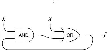
Although counter-intuitive, could a combinational circuit be designed with feed-back paths?
“It can’t be done.”
One might argue that with feedback, we cannot determine the output values without knowing the current state, and so the circuit must be sequential. This view is illustrated in Figure 1.4.
PSfrag replacements
f
1f
2f
3f
4Figure 1.4: A circuit with feedback. How can we determine the output f without knowing the value of y in a feedback path?
PSfrag replacements
f
1f
2f
3f
4Figure 1.5: A (useless) cyclic combinational circuit.
Recall that the output of anANDgate is 0 iff either input is 0; the output of an OR gate is 1 iff either input is 1. Consider the two possible values of x. On the one hand, if x= 0 then the output of the AND gate is fixed at 0; the input from the ORgate has no influence, as shown in Figure 1.6 (a). On the other hand, if x = 1 then the output of the ORgate is fixed at 1; the input from the AND gate has no influence, as shown in Figure 1.6 (b). Although useless, this circuit is cyclic and combinational. The value of the outputf is determined by the current input valuex(actuallyf =x) regardless of the prior state and independently of all timing assumptions.
PSfrag replacements
f
1f
2f
3f
4PSfrag replacements
f
1f
2f
3f
4(a) (b)
Figure 1.6: The circuit of Figure 1.5 with (a)x= 0, and (b) x= 1.
“It probably can be done, but it’s not worth doing.”
5
PSfrag replacements
f
1f
2f
3f
4Figure 1.7: A cyclic combinational circuit due to Rivest [35].
shown in Figure 1.8. We compute
f1 = x1y
f2 = x2 +f1 = x2+x1y
f3 = x3f2 = x3(x2+x1y)
f4 = x1 +f3 = x1+x3(x2+x1y) = x1+x2x3
f5 = x2f4 = x2(x1+x2x3) = x2(x1+x3)
f6 = x3 +f5 = x3+x2(x1+x3) = x3+x1x2.
(Here addition represents OR and multiplication represents AND.) We see that f4, and consequently f5 and f6, do not depend upon the unknown value. Thus, we
compute
f1 = x1f6 = x1(x3 +x1x2) = x1(x2+x3)
f2 = x2+f1 = x2 +x1(x2+x3) = x2+x1x3
f3 = x3f2 = x3(x2 +x1x3) = x3(x1+x2).
Each output depends on the current input values, not on the prior values, and so the circuit is combinational.
PSfrag replacements
f
1f
2f
3f
4) ( 2 3
1 x x
x +
f
1f
2f
3f
4Figure 1.9: With fan-in two gates, two gates are needed to compute x1(x2+x3).
Unlike the circuit in Figure 1.5, this one computes something useful. The six output functions are distinct, and each depends on all three input variables. Moreover, we can show that this cyclic circuit hasfewergates than any equivalent acyclic circuit. To see this, note that any acyclic configuration contains at least one gate producing an output function that does not depend on the output of any other gate producing an output function. (If this were not the case, then every output gate would depend upon another and so the circuit would be cyclic.) With fan-in two gates, it takes two gates to compute any one of the six functions by itself. This is illustrated in Figure 1.9. We conclude that an acyclic implementation of the six functions requires seven gates, compared to the six in the cyclic circuit.
“I knew it was a good idea all along!”
7
1.2
Prior Work
1.2.1
The Early Era
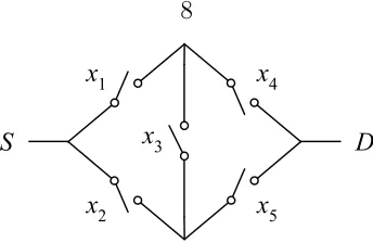
Gates are a convenient abstraction, introduced for digital electronic circuits. In an earlier era, people studied switching circuits, built from electro-mechanical relays. A relay is device that conducts current if it is set to “on” (corresponding to a logical input of 1), and does not conduct current if it is set to “off” (corresponding to a logical input of 0). The device does not have an intrinsic direction; it will conduct current in either direction. The symbol for a relay is shown in Figure 1.10 A switching circuit evaluates to logical 1 if there is a conducting path between a designated “source” point and a designated “drain” point.
PSfrag replacements
f
1f
2f
3f
4Figure 1.10: A contact relay.
Switching circuits were the subject of seminal papers by Claude Shannon: the analysis of such circuits in 1938 [39] and the synthesis of such circuits in 1949 [40]. The circuits of Shannon’s day often had cyclic topologies. Since relays are directionless, cycles do not pose any problem. Consider the bridge circuit shown in Figure 1.11. The logical function implemented between points Sand Dis
f(x1, x2, x3, x4, x5) =x1x4+x1x3x5+x2x5+x2x3x4.
It may be shown this circuit has fewer switches than is possible with an acyclic topology.
It was accepted that cycles were an important feature in the design of switching circuits. In 1953, Shannon described a cyclic switching circuit with 18 contacts that computes all 16 Boolean functions of two inputs, and he proved that this circuit is optimal [41].
PSfrag replacements
f
1f
2f
3f
4Figure 1.11: A switching circuit with a cyclic topology.
switching elements. It is equivalent to a form of binary decision diagram now known as a zero-suppresseddecision diagram [30]. In this context, Short argued that cyclic designs are necessary for the minimal forms.
In recent years, binary decision diagrams have come to the fore as perhaps the most successful data structure for representing Boolean functions [7]. Short’s work suggests that feedback might be useful in optimizing binary decision diagrams, a topic of future research that we return to in Chapter 6.
In the 1960’s, as the research community was shifting its focus to the now-familiar model of of directed logic gates (AND, OR, NOT, etc.), researchers naturally pon-dered the implication of cyclic designs. In 1963, McCaw presented a thesis for his Engineer’s Degree titled “Loops in Directed Combinational Switching Networks” [26]. He begins with an example, the cyclic circuit shown in Figure 1.12 consisting of two AND gates and two ORgates, with five inputs and two outputs. His argument for combinationality is in the same vein as that given above for Rivest’s circuit:
f1 = a+b+x(c+d+ ¯xf1) = a+b+x(c+d)
f2 = c+d+ ¯x(a+b+xf2) = c+d+ ¯x(a+b).
9
PSfrag replacements
f
1f
2f
3f
4Figure 1.12: A cyclic combinational circuit due to McCaw.
In 1970, Kautz (Short’s Ph.D. advisor at Stanford) presented a short paper on the topic of feedback in circuits with logic gates [17]. He described a cyclic circuit consisting of 6 fan-in twoNOR gates with three inputs and three outputs. Although plausible, his circuit is not combinational according to the rigorous model that we propose. (It assumes that all wires have definite Boolean values at the outset.)
In 1971, Huffman discussed feedback in linear threshold networks. He claimed that an arbitrarily large number of input variables can be complemented in a network con-taining a single NOT element, provided that feedback is used [15]. This improved upon an earlier result by Markov, demonstrating that k NOT elements suffice to generate the complements of 2k−1 variables [25]. As with Kautz’s example,
Huff-man’s is not combinational in the sense that we understand it. Still, in an insightful commentary on his and Kautz’s work, he hinted at the possible implications,
“ At this time, these[cyclic]examples are isolated ones. They do, however, provide tantalizing glimpses into an imaginable area of future research.”
we analyze Rivest’s construction, present variants and extensions, and generalize the argument of optimality
1.2.2
The Later Era
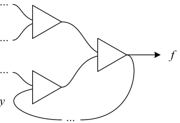
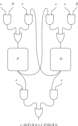
More recently, practitioners observed that cycles sometimes occur in combinational circuits synthesized from high-level descriptions. In such examples, feedback either is inadvertent or else is carefully contrived. For instance, occasionally it is intro-duced during resource-sharing optimizations at the level of functional units [47]. In these circuits, there is explicit “control” circuitry governing the interaction between “functional” units.
Consider the example in Figure 1.13. Here we have an input word X (that is, a bundle of wires carrying several bits of information) and a control input c. There are two functional units, F and G, each of which performs a word-wise operation. If cis 1, then the circuit computes
G(F(X)),
while if it is 0, it computes
F(G(X)).
Suppose that X = (x1, . . . , xn) is an n-bit word, representing the integer
x1+ 2x2+· · ·+ 2n−1xn.
Here F(X) might be an exponentiation
F(X) = 2X mod 2n,
and G(X) might be a left-shift (division by 2),
G(X) =
X 2
.
exponen-11 tiation followed by a left-shift.
)) ( ( ))
(
(F X c F G X G
c⋅ + ⋅
PSfrag replacements
f
1f
2f
3f
4Figure 1.13: Functional units connected in a cyclic topology.
1.3
Overview
In the realm of digital circuits, researchers seems to fall into two camps. On the one hand, there are the theoreticians, working in the field of circuit complexity. They are preoccupied with classifyingand characterizing problems in general terms. They discuss the relationships among complexity classes, and prove bounds on the size of circuits. On the other hand, there are the practitioners, working in the field of electronic design automation. They strive to obtain the best circuits that they can, given the computational resources at their disposal. However, they rarely speak of optimaldesigns. The true optimum according to any criteria – be it area, delay, power – is generally unknowable to them.
1.3.1
Theory
In the first half of this dissertation, we wear the theoretician’s mantle. In Chapter 2 we describe our circuit model, and present a framework for analysis. In Chapter 3, we present theoretical justification for the claim that the optimal form of some circuits requires cyclic topologies. We exhibit families of cyclic circuits that are optimal in the number of gates, and we prove lower bounds on the size of equivalent acyclic circuits. For instance, the cyclic circuit in Figure 1.14 consists of three “complex” gates, each with fan-in 6. We show that this circuit implements three distinct functions, f1,
f2 and f3, each depending on all 12 variables a, . . . , l. We then argue that an acyclic
circuit implementing the same functions requires at least five fan-in 6 gates.
Our lower bound is based on a simple fan-in argument: in order to compute a function that depends on a certain number of variables using gates with a certain fan-in, we require a tree of at least a certain size. This is perhaps the weakest lower bound than one can conceive of on a circuit’s size. This suggests that feedback may be more powerful than we can show.
13
3 1 a(cegi) af
f = ⊕
2 1 2
1
3 kl af b f abf f
f = ⊕ ⊕ ⊕
3 2 b(d fhj) bf
f = ⊕
1
g
2
g
3
g
PSfrag replacements
f
1f
2f
3f
4Figure 1.14: Cyclic circuit with inputs a, . . . , l and outputs f1, f2, f3. (⊕ represents
XOR.)
1.3.2
Practice
In the second half of the dissertation, we wear the practitioner’s mantle. In Chapter 5 we describe a general methodology for synthesizing cyclic combinational circuits, and compare our results to those produced by state-of-the art logic synthesis tools.
Consider the example shown in Figure 1.15, ubiquitous in introductory logic de-sign courses: a 7-segment display decoder. The inputs are four bits, x0, x1, x2, x3,
specifying a number from 0 to 9. The outputs are 7 bits, a, b, c, d, e, f,g, specifying which segments to light up in a display – such as that of a digital alarm clock – to form the image of this number.
With our synthesis methodology, we arrive at the network shown in Figure 1.16, with the ordering illustrated. This network translates into a cyclic circuit with 27 fan-in two gates. In contrast, standard synthesis techniques produce an acyclic circuit with 32 fan-in two gates.
inputs outputs
x3 x2 x1 x0 Digit a b c d e f g
0 0 0 0 0 1 1 1 0 1 1 1
0 0 0 1 1 0 0 0 0 0 1 1
0 0 1 0 2 0 1 1 1 1 1 0
0 0 1 1 3 0 0 1 1 1 1 1
0 1 0 0 4 1 0 0 1 0 1 1
0 1 0 1 5 1 0 1 1 1 0 1
0 1 1 0 6 1 1 0 1 1 0 1
0 1 1 1 7 0 0 1 0 0 1 1
1 0 0 0 8 1 1 1 1 1 1 1
1 0 0 1 9 1 0 1 1 0 1 1
PSfrag replacements
f
1f
2f
3f
4Figure 1.15: 7-Segment Display Decoder.
values of the functions – the circuit delay? We refer to this task as timing analysis. Khrapchenko was the first to recognize that depth and delay in a circuit are not equivalent concepts [18]. There may existfalse paths, that is to say, topological paths that are never sensitized. So-called “exact” algorithms for timing analysis consider the presence of false paths; these provide the requisite tool for the analysis of cyclic circuits. For a cyclic circuit, we can say that it is combinational if all cycles are false; the sensitized paths in the circuit never bite their own tail to form true cycles.
Our synthesis program can routinely tackle designs with, say 50 inputs and 30 outputs. For circuits of this size, a exhaustive approach to analysis – that is to say, checking every input assignment – is not feasible: withn variables there would be 2n
input combinations. In Chapter 4 we describe efficient algorithms for analysis based onsymbolictechniques, using flexible data structures calledbinary decision diagrams. Our analysis considers topological aspects of the design, for instance sub-dividing the problem into strongly connected components.
15
a = ¯x3x¯0¯c+ ¯x1c
b = ¯x0e
c = ¯x3x2x0 + ¯x2(x3x¯1+e)
d = (x3+x2)a+x1e
e = ¯x2(x1+ ¯x0)f+ ¯x3f¯
f = (¯x2+ ¯x1x¯0)g+ ¯x3¯a
g = ¯x3¯b+a
a
g
d f
b c
e
PSfrag replacements
f1 f2 f3 f4
Figure 1.16: A cyclic network for the example in Figure 1.15.
were optimized significantly, with improvements of up to 30% in the area and up to 25% in the delay.
Theoreticians may dismiss optimizations of this sort as inconsequential:
“Saving a few gates in the design of a 7-segment decoder doesn’t prove anything”.
Practitioners may dismiss the theoretical results as contrived:
“Asymptotic bounds don’t help me one bit in designing real circuits.”.
Chapter 2
Framework
Make everything as simple as possible without making anything too simple.
– Albert Einstein (1879–1955)
The concepts discussed in this dissertation are not tied to any particular physical model or computing substrate. For the core ideas in Chapter 4 and Chapter 5, the exposition is at a symbolic level, that is to say, in terms of Boolean expressions. However, we first postulate an underlying structural model, consisting of gates and wires, and discuss analysis in an explicit sense – in terms of signal values.
2.1
Circuit Model
We work with digital abstraction of 0’s and 1’s. Nevertheless, our model recognizes that the underlying signals are, in fact, analog: each signal is a continuous real-valued function of time s(t), corresponding to a voltage level. For analysis, we adopt a ternary framework, extending the set of Boolean values = {0,1} to the set of ternary values ={0,1,⊥}. The logical value of an analog signal is obtained by the
mapping
logical[s(t)] =
0 if s(t)< Vlow
1 if s(t)> Vhigh
17
whereVlow and Vhigh are real values demarcating the range corresponding to Boolean
0 and Boolean 1, respectively. Clearly, Vhigh must be strictly greater than Vlow. The
third value, ⊥, indicates that the signal is ambiguous. For the purposes of analysis, ⊥ is used in a broader sense: it denotes a signal value that is unknown. This signal may be Boolean 0, Boolean 1, or some ambiguous value – we simply do not know.
The idea of three-valued logic for circuit analysis is well established. It was orig-inally proposed for the analysis of hazards in combinational logic [13], [50]. Bryant popularized its use for verification [8], and it has been widely adopted for the analysis of asynchronous circuits [9]. For a theoretical treatment, see [29].
A circuit consists ofgatesconnected by wires. Each gate has one or more inputs and a single output. The symbols for common gates are shown in Figure 2.1. A bubble is used to indicate that an input or output is negated, as illustrated in Figure 2.2. PSfrag replacements
f
1f
2f
3f
4Figure 2.1: Symbols for different types of gates. PSfrag replacements
f
1f
2f
3f
4Figure 2.2: Bubbles on the inputs or the output of a gate indicate negation. Here z =NOT(OR(NOT(x), y)).
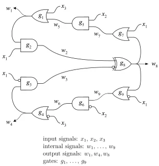
An example of a circuit is shown in Figure 2.3. Even though a wire may split in our diagrams, as is the case with wirew8 in Figure 2.3, conceptually there is a single
instance of it.
• The circuit accepts signals x1, . . . , xm, ranging over {0,1}, called theprimary
• The gates in the circuit produce internal signals, w1, . . . , wn ranging over
{0,1,⊥}.
• A subset of the set of internal signals is designated as the set of primary outputs.
PSfrag replacements
f
1f
2f
3f
4input signals: x1,x2, x3
internal signals: w1, . . . , w9
output signals: w1, w4, w8
gates: g1, . . . , g9
Figure 2.3: An example of a circuit, consisting of gates and wires.
2.1.1
Functional Behavior
In the digital realm, a gate implements a Boolean function, i.e., a mapping from Boolean inputs to a Boolean output value,
19
The set of inputs to a gate are called its fan-in set. When we say a “fan-in k” gate, we mean a gate with fan-in set of cardinality k. The set of gates that are attached to a gate output are called its fan-out set. The truth tables for fan-in two AND, OR and XOR gates, as well as a fan-in oneNOT gate, are shown Figure 2.4.
x y AND(x, y) OR(x, y) XOR(x, y)
0 0 0 0 0
0 1 0 1 1
1 0 0 1 1
1 1 1 1 0
x NOT(x)
0 1
1 0
Figure 2.4: Truth table for common gates.
2.1.2
Temporal Behavior
We characterize the temporal behavior of a gate by a single parameter, a bound on its delay td.
For a gate characterized by a mapping g, if the inputs assume the values y1(t), . . . , yk(t) at timet, and subsequently do not change, then the output
assumes the valueg[y1(t), . . . , yk(t)] at time no later than t+td, and does
not change.
Further, we assume that the wires have zero propagation delay. More realistic models for timing analysis can readily be incorporated within our framework; we neglect such details here in order to focus on the conceptual aspects.
2.2
Analysis Framework
Analysis of anacycliccircuit is transparent. We first evaluate the gates connected only to primary inputs, and then gates connected to these and primary inputs, and so on, until we have evaluated all gates. For instance, in the circuit of Figure 1.2 in the Introduction, we first evaluate g1 and g2, then g3, then g4 and g5. At each step,
we only evaluate a gate when all of its input signals are known. The previous values of the internal signals do not enter into play.
In a cyclic circuit, there are one or more strongly connected components. Recall that in a directed graphG, a strongly connected component is an induced subgraph S ⊆Gsuch that
• there exists a directed path between every pair of nodes in S;
• for every nodesinS and every noden outside ofS, if there exists a path froms ton (fromn tos) then there is no path fromn tos (from ston, respectively).
We analyze each strongly connected component separately.
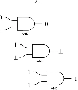
At the outset, with only the primary inputs fixed at definite values, each gate in a strongly connected component has some unknown/undefined inputs (valued ⊥). Nevertheless, for each such gate we can ask: is there sufficient information to conclude that the gate output is 0 or 1, in spite of the ⊥ values? If yes, we assign this value as the output; otherwise, the value ⊥ persists. For instance, with an AND gate, if the inputs include a 0, then the output is 0, regardless of other ⊥ inputs. If the inputs consist of 1 and ⊥values, then the output is ⊥. Only if all the inputs are 1 is the output 1. This is illustrated in Figure 2.5. Input values that determine the gate output are called controlling.
2.2.1
Ternary Extension
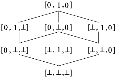
For the set {0,1,⊥}, we define a partial ordering
21
⊥
⊥ ⊥
PSfrag replacements
f
1f
2f
3f
4Figure 2.5: An AND gate with 0, 1, and ⊥inputs.
with 0 and 1 not comparable. For vectors Y = (y1, . . . , yn) and Z = (z1, . . . , zn), we
define the ordering coordinate-wise:
Y vZ if yi vzi for all i= 1, . . . , n.
For instance, if Y = (⊥,1,⊥,0), and Z = (1,1,1,0) then Y v Z. However, if Y = (⊥,1,⊥,0) andZ = (1,1,1,⊥) then Y and Z are not comparable.
We define the partial join V = (v1, . . . , vn) =Y tZ as:
vi =
a if yi =zi =a for some a∈ {0,1},
b if {yi, zi}={b,⊥}for some b ∈ {0,1},
⊥ else.
for all i = 1, . . . , n. For instance, if Y = (⊥,1,⊥,0), and Z = (1,1,1,⊥) then Y tZ = (1,1,1,0).
Within the ternary framework, a gate performs a mapping from ternary values to ternary values,
g0
:{0,1,⊥}k→ {0,1,⊥}.
We call this mapping the ternary extension of g. Given a Boolean mapping g, the
{0,1,⊥}k,
g0(Y) =
0 if g(Z) = 0 for each Z ∈ {0,1}k, where Y vZ,
1 if g(Z) = 1 for each Z ∈ {0,1}k, where Y vZ,
⊥ else.
A similar definition of the ternary extension is found in [9]. The truth-tables for the ternary extensions of fan-in two AND, OR and XOR gates, as well as a fan-in one NOT gate, are shown in Figure 2.6.
x y AND(x, y) OR(x, y) XOR(x,y)
0 0 0 0 0
0 1 0 1 1
0 ⊥ 0 ⊥ ⊥
1 0 0 1 1
1 1 1 1 0
1 ⊥ ⊥ 1 ⊥
⊥ 0 0 ⊥ ⊥
⊥ 1 ⊥ 1 ⊥
⊥ ⊥ ⊥ ⊥ ⊥
x NOT(x)
0 1
1 0
⊥ ⊥
Figure 2.6: Ternary extensions for common gates.
2.2.2
Fixed Point
The goal of functional analysis is to determine what output values a circuit produces in response to Boolean input values. Of course, if the circuit is cyclic, we cannot be sure that it settles to a stable state. Consider the inverter ring shown in Figure 2.7. With x= 1, the ring will probably oscillate, with the output z alternating between 0 and 1, as shown in Figure 2.8. Within the ternary framework, all instability is hidden beneath the ⊥ values. This is illustrated with the inverter chain in Figure 2.9.
23
PSfrag replacements
f
1f
2f
3f
4Figure 2.7: An inverter ring.
outcome – which internal wires are assigned definite values, and what these values are – is the same regardless. The analysis terminates at a fixed point: in this state, every gate evaluation agrees with the value on its output wire, so there are no further changes. Of course, the term “fixed point” is somewhat paradoxical: with ⊥ values, the state includes signals that are potentially unstable.
PSfrag replacements
f
1f
2f
3f
4Figure 2.8: In the Boolean framework, the inverter ring oscillates.
⊥ ⊥ ⊥
⊥
PSfrag replacements
f
1f
2f
3f
4Figure 2.9: In the ternary framework, the values are unknown/undefined.
Theorem 2.1 With all the internal signals assigned an initial value ⊥, for a given
set of Boolean values applied to the inputs and held constant, the analysis terminates
at a unique fixed point.
Proof: Call the values assumed by the internal variables W = (w1, . . . , wn) the
state. Beginning from the initial state W0 = (⊥, . . . ,⊥), the circuit evolves through
a sequence,
W0, W1, W2, . . .
ordered,
W0 vW1 vW2 v. . .
Since the number of states is finite, clearly the computation terminates at some fixed point. This is illustrated in Figure 2.10.
It remains to show that this fixed point is unique. To do so, we argue that the order of updates is irrelevant. Indeed, from a given state W, if we have a choice of immediate successor states Wi and Wj, then the partial join Wk = Wi t Wj
exists and is an immediate successor state to both Wi and Wj. This is illustrated in
Figure 2.11. With the initial state (⊥, . . . ,⊥) as the base case, a simple inductive argument suffices to show that all states have a common successor. This common
successor must be a fixed point. 2
PSfrag replacements
f
1f
2f
3f
4Figure 2.10: The computation terminates at a fixed point.
PSfrag replacements
f
1f
2f
3f
425
2.2.3
Explicit Analysis
The analysis strategy for specific Boolean input values might be termed simulation: we apply inputs and follow the evolution of the circuit. The goal of functional analysis is to determine what values appear; the goal of timing analysis is to determine whenthese values appear.
For functional analysis, Theorem 2.1 tells us that the gates may be evaluated in any order. We simply apply the inputs and follow the signals as they propagate; gates are evaluated when new signals arrive. Once a gate evaluates to a definite Boolean value, it is not evaluated again. Once the analysis terminates, if there are ⊥ values on the outputs, we conclude that the circuit does not behave combinationally.
For timing analysis, we establish an upper bound on the arrival times of definite Boolean values for internal signals. We always evaluate gates in the order that signals arrive, ensuring that we know the earliest time that a signal value becomes known. When evaluating a gate, we use only present and past input values, not future values. We illustrate analysis with a collection of examples: first two (acyclic) circuit fragments; then a non-combinational cyclic circuit; and finally a combinational cyclic circuit. We assume that all gates have unit delay, and that the primary inputs arrive at time 0.
Example 2.1
Consider the circuit fragment shown in Figure 2.12. It consists of four gates: an
AND gate g1, an ORgate g2, an AND gate g3, and anOR gate g4:
g1(x1, y1) = x1y1,
g2(x2, y2) = x2 +y2,
g3(x3, y3) = x3y3,
g4(x1, y4) = x1 +y4.
PSfrag replacements
f
1f
2f
3f
4Figure 2.12: A circuit fragment.
there exists a path from pointAto pointB in this circuit. However, from a functional standpoint, this path is never sensitized. To see this, consider specific input values:
• With x1 = 0, the path is blocked at gate g1.
• With x2 = 1, the path is blocked at gate g2.
• With x3 = 0, the path is blocked at gate g3.
• With x1 = 1, the path is blocked at gate g4.
For any combination of input values, we know what value appears at pointB, and how long it takes for this value to appear, regardless of the signal at point A. Assuming that the gates g1, g2, g3 and g4 have uniform delay bounds of t1, t2, t3, and t4,
respectively, we can assert:
• With x1 = 1, a value of 1 appears after t4 time units.
• With x1 = 0, and x3 = 0, a value of 0 appears after t3+t4 time units.
• With x1 = 0, x3 = 1, and x2 = 1, a value of 1 appears after t2 +t3 +t4 time
units.
• With x1 = 0, x3 = 1, and x2 = 0, a value of 0 appears after t1 +t2 +t3 +t4
time units.
Further assuming a unit delay model (i.e., t1 = t2 = t3 = t4 = 1), we obtain the
27
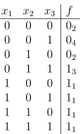
x1 x2 x3 f
0 0 0 02
0 0 1 04
0 1 0 02
0 1 1 13
1 0 0 11
1 0 1 11
1 1 0 11
1 1 1 11
Table 2.1: Analysis of the circuit fragment in Figure 2.12.
Example 2.2
Consider the circuit shown in Figure 2.13, consisting of an AND gate g1, anOR gate g2, and an AND gate g3, in a cycle. By inspection, note that ifx1 = 0 then f1
assumes value 0 after one time unit; ifx2 = 1 thenf2 assumes value 1 after one time
unit; and if x3 = 0 then f3 assumes value 0 after one time unit. But what happens
if x1 = 1, x2 = 0 and x3 = 1? In this case, all the outputs equal ⊥, as illustrated in
Figure 2.14. The outcome for all eight cases is shown in Table 2.2.
PSfrag replacements
f
1f
2f
3f
4Figure 2.13: A non-combinational cyclic circuit.
⊥ ⊥ ⊥
PSfrag replacements
f
1f
2f
3f
4x1 x2 x3 f1 f2 f3
0 0 0 01 02 01
0 0 1 01 02 03
0 1 0 01 11 01
0 1 1 01 11 12
1 0 0 02 03 01
1 0 1 ⊥ ⊥ ⊥
1 1 0 02 11 01
1 1 1 13 11 12
Table 2.2: Analysis of circuit in Figure 2.13.
In general, we would reject this circuit, since its outputs are not defined for the input assignment x1 = 1, x2 = 0 and x3 = 1. However, if this particular assignment
is in the “don’t care” set, then the design would be valid.
Example 2.3
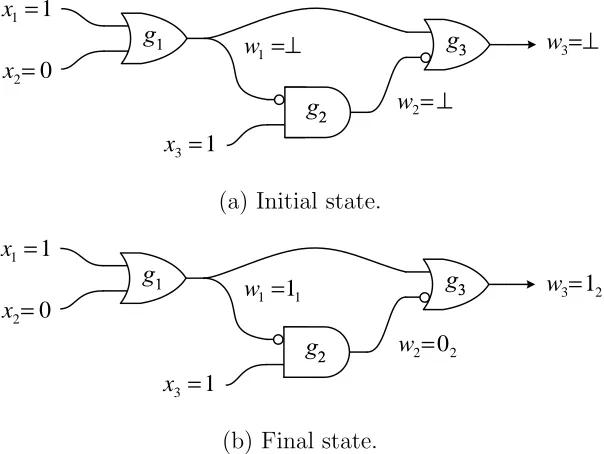
Consider the circuit in Figure 2.15 (a).
• Of the three gates, we see that initially only g1 evaluates to a definite value,
w1 =g1(x1, x2) =OR(1,0) = 1.
We set the arrival time of w1 to be
t1 = 1.
• With w1 defined, we see thatg2 evaluates to a definite value,
w2 =g2(w1, x2) =AND(NOT(1),1) = 0.
We set arrival time of w2 to be
t2 = 1 +t1 = 2.
• At this point in the execution of the algorithm, w1 and w2 have been assigned
29
w3 =g3(w1, w2) =OR(1,NOT(⊥)) = 1.
We set the arrival time of w3 to be
t3 = 1 +t1 = 2.
The final values of w1, w2, w3 are shown in Figure 2.15 (b). Subscripts indicate the
arrival times. ⊥ = 1 w ⊥ = 2 w ⊥ = 3 w 1 1 = x 1 3 = x 0 2= x PSfrag replacements
f
1f
2f
3f
4(a) Initial state.
1 1 =1
w
2 2=0
w
2 3=1
w 1 1= x 1 3 = x 0 2= x PSfrag replacements
f
1f
2f
3f
4(b) Final state.
Figure 2.15: Example 2.3 Subscripts on the values of the internal variables indicate the arrival times.
The salient point of this example is that the algorithm tracks the arrival times of signals, and establishes the earliest possible set of controlling signals. If gate g3 had
been evaluated after bothw1 and w2 had been determined, we might have concluded
that its arrival time was 3 time units instead of 2.
Example 2.4
Consider the circuit in Figure 2.16. Suppose that we apply inputs x1 = 1, x2 =
0, x3 = 1, as shown in Part (a). Gates g1, g3, g5 and g7 produce outputs of 1, 0, 0,
and 1, respectively, after one time unit. Gate g2 produces an output of 1 after two
an output of 0 after four time units. Gateg6 produces an output of 0 after five time
units. Finally, gate g4 produces an output of 0 after six time units. The circuit after
six time units is shown in Figure 2.16 (b).
The analysis for all eight input combinations is summarized in Table 2.3. We see that the maximum delay of the circuit is six time units.
x1 x2 x3 g1 g2 g3 g4 g5 g6 g7 g8 g9
0 0 0 02 01 12 11 01 12 04 03 11
0 0 1 11 01 14 13 01 12 06 05 11
0 1 0 06 01 12 11 05 01 04 03 11
0 1 1 11 01 03 02 16 01 15 14 11
1 0 0 02 03 01 11 01 16 11 14 15
1 0 1 11 12 01 06 01 05 11 03 04
1 1 0 13 14 01 11 12 01 11 05 06
1 1 1 11 12 01 02 12 01 11 03 04
Table 2.3: Analysis summary for the circuit of Figure 2.3. Subscripts on the output values indicate arrival times.
2.2.4
Complexity
In the analysis, we evaluate a gate whenever a new Boolean signal arrives on one of its inputs. In the worst case, we could evaluate a gate with fan-in d as many as d times. Given a circuit with m primary inputs and n gates, each with fan-in d, there are O(d n) gate evaluations. In addition, for timing analysis, we must maintain a sorted list of arrival times. This contributes a complexity factor of O(n log2 n).
We could perform the analysis explicitly for every assignment of input values. However, such an exhaustive approach is simply not tractable for most real circuits: with n variables there would be 2n input combinations to analyze separately. In
31 ⊥ ⊥ ⊥ ⊥ ⊥ ⊥ ⊥ ⊥ ⊥ PSfrag replacements
f
1f
2f
3f
4(a) time t= 0
PSfrag replacements
f
1f
2f
3f
4(b) time t = 6
Figure 2.16: The circuit of Figure 2.3 with inputs x1 = 1, x2 = 0, x3 = 1. Subscripts
Chapter 3
Theory
In theory there is no difference between theory and practice, but in practice
there is. – Yogi Berra (1925– )
Theoreticians are preoccupied with classifying and characterizing problems in general terms. They discuss the relationships among complexity classes, and prove bounds on the size of circuits. However, somewhat to their embarrassment, they offer very little help in proving or disproving the optimality of specific circuits. There have been a handful of papers, dating back to the 1960’s, describing approaches for finding optimal multi-level circuit designs [10], [11], [20], but these have limited applicability: the largest circuits that these methods can hope to tackle have 4 (or perhaps 5) input variables.
Lower bounds on circuit size are notoriously difficult to establish. In fact, such proofs are related to fundamental questions in computer science, such as the separa-tion of the P and N P complexity classes. (To prove that P 6= N P it would suffice to find a class of problems in N P that cannot be computed by a polynomially sized circuit.) Much of the recent work in circuit complexity has been spurred by these open problems [1].
33
Given these limitations, how can we hope to justify our general claim that feedback can be used to optimize circuits? In this section, we assume the theoretician’s mantle and provethat some cyclic designs are smaller than equivalent acyclic ones, based on the best lower-bound techniques that we know.
3.1
Criteria for Optimality
Any assertion of optimality rests on a restricted circuit model. Indeed, with gates of arbitrary size and complexity, any function can be implemented with a single “gate.” We restrict the scope of gates in two ways. The first way is to bound the fan-in, as shown in Figure 3.1 (a). Each gate can have at most dinputs, for some finite d. The second way is to restrict the type of gate. For instance, we can limit ourselves to so-called AON gates: AND gates with the inputs and output possibly negated. An example of such a gate is shown in Figure 3.1 (b). The general form of the Boolean function realized by an AON gate is
g(x1, x2, . . . , xd) = (x1⊕c1)·(x2 ⊕c2)· · ·(xd⊕cd)⊕cd+1,
where c1, . . . , cd+1 are arbitrary choices of 0 and 1. (Multiplication represents AND,
addition represents OR, and ⊕ represents XOR.) The fan-in d may or may not be limited.
PSfrag replacements
f
1f
2f
3f
4
PSfrag replacements
f
1f
2f
3f
4(a) (b)
Figure 3.1: Restricting the scope of gates. (a) Bound the fan-in. (b) Use AND gates (with the inputs and output possibly negated).
we need not concern ourselves with simplifying the expressions. Furthermore, the dependence of a function on its variables is explicit. See Appendix A for a discussion of this representation.
Our general strategy in the following constructions is to present a cyclic circuit that is optimal in the number of gates, and then prove a lower bound on the size of any acyclic circuit implementing the same functions. The argument for the optimality of the cyclic circuit rests on two properties:
Property 3.1 Each of the output functions depends on all its variables.
Property 3.2 The output functions are distinct.
The cyclic circuit is shown to be optimal according to the following trivial claim (true regardless of the gate model):
Claim 3.1 A circuit implementingm distinct functions consists of at least m gates.
3.2
Fan-in Lower Bound
Our lower bound on the size of an acyclic circuit is formulated as a fan-in argument. The essence of the argument was presented by Rivest [35], although we present it in a more general form.
A circuit can only compute a function of a given set of input variables if it “sees” all of them. For example, in Figure 3.2, gate g2 can compute a function ofx1, x2 and
x3; g1 cannot compute a function ofx3 since it does not see x3. In an acyclic circuit,
there is a partial ordering among the gates: if a gategi depends on a gate gj, directly
or indirectly, then gj cannot depend on gi, directly or indirectly. With a partial
35
PSfrag replacements
f
1f
2f
3f
4Figure 3.2: A gate can only compute functions of variables that it “sees”.
Claim 3.2 An acyclic circuit implementing m distinct output functions, each de-pending on v input variables, consisting of gates with fan-in at most d has at least
v−1 d−1
+m−1
gates.
Proof: Consider a connected directed acyclic graph (DAG). Call nodes with no in-coming edges leaves, and all other nodes internal nodes. We show, by a simple inductive argument, that a connected DAG with k internal nodes, each with in-degree at most d, has at most k(d− 1) + 1 leaves. Obviously, a graph consisting of a single such internal node has at most d leaves. Suppose an internal node with in-degree at most d is added to a connected DAG. If the resulting graph is to be a connected DAG, the new node can replace an existing leaf or it can be attached to an existing internal node. The former case is illustrated with node g1 in Figure 3.3,
and the latter with node g2. In both cases there is a net gain of at most d−1 leaves.
We conclude that connected DAG with k internal nodes has at most
d+ (k−1)(d−1) = k(d−1) + 1
PSfrag replacements
f
1f
2f
3f
4Figure 3.3: Adding a node with in-degree d to a connected DAG results in net gain of at most d−1 leaves.
v ≤k(d−1) + 1,
the number of internal nodes k is bounded by
k ≥
v−1 d−1
.
Now, in an acyclic circuit implementingmoutput functions, at least one of the output functions depends on no other. By the argument above, this output function requires at least
v−1 d−1
gates. With distinct output functions, each output function must emanate from a different gate, so at least m−1 gates are required to implement the remaining m−1
37
3.3
Improvement Factor
Suppose that we have a cyclic circuit with m gates, each with fan-in at most d, that implementsm distinct functions, each of which depends on allv input variables. Call the improvement factor the ratio of size of the cyclic circuit to the lower bound on the size of the acyclic circuit:
size of cyclic size of acyclic =
m v−1
d−1
+m−1.
With an improvement factor of C, we can say that our cyclic circuit is C times the size of any equivalent acyclic circuit.
Claim 3.3 The improvement factor is bounded below by 12.
Proof: For a given d, the improvement factor is minimized if the term
v−1 d−1
in the denominator is maximized. Now, the number of variables v in a cyclic circuit is at most m(d−1), and this is achieved if all the gates have fan-in d. For such a circuit,
m
m− 1
d−1
+m−1 = m 2m−1 ≥
1 2.
2
3.4
Examples
PSfrag replacements
f
1f
2f
3f
4Figure 3.4: A cyclic combinational circuit with 3 inputs, due to Rivest [35].
Setting x1 = 0 we have
f1|¯x1 = 0,
f2|¯x1 = f1+x2 = x2, f3|¯x1 = f2x3 = x2x3, f4|¯x1 = f3+ 0 = x2x3, f5|¯x1 = f4x2 = x2x3, f6|¯x1 = f5+x3 = x3.
All outputs assume definite Boolean values. For gate g4, an OR gate, x1 = 1 is a
controlling value. Setting x1 = 1, we have
f4|x1 = 1,
f5|x1 = f4x2 = x2, f6|x1 = f5+x3 = x2 +x3, f1|x1 = f61 = x2 +x3, f2|x1 = f1+x2 = x2 +x3, f3|x1 = f2x3 = x3.
Again, all outputs assume definite Boolean values. Since x1 must either have value 0
39 functions from these two cases:
f1 = ¯x1 ·f1|x¯1 + x1·f1|x1 = ¯x1 ·0 + x1·(x2+x3) = x1(x2+x3) f2 = ¯x1 ·f2|x¯1 + x1·f2|x1 = ¯x1 ·x2 + x1·(x2+x3) = x2+x1x3 f3 = ¯x1 ·f3|x¯1 + x1·f3|x1 = ¯x1 ·x2x3 + x1·x3 = x3(x1+x2) f4 = ¯x1 ·f4|x¯1 + x1·f4|x1 = ¯x1 ·x2x3 + x1·1 = x1+x2x3 f5 = ¯x1 ·f5|x¯1 + x1·f5|x1 = ¯x1 ·x2x3 + x1·x2 = x2(x1+x3) f6 = ¯x1 ·f6|x¯1 + x1·f6|x1 = ¯x1 ·x3 + x1·(x2+x3) = x3+x1x2.
Rivest presented a more general version of this circuit. For any odd integer n greater than 1, the general circuit consists of n two-input AND gates alternating with n two-input OR gates in a single cycle, with inputs x1, . . . , xn repeated, as shown in Figure 3.5. Analyzing the general circuit in the same manner as above, we find that
PSfrag replacements
f
1f
2f
3f
4Figure 3.5: A cyclic combinational circuit with n inputs (for any odd n ≥ 3) due to Rivest.
it implements the functions
f1 = x1(xn+xn−1(· · ·(x3 +x2)· · ·))
f2 = x2 +x1(xn+· · ·(x4x3)· · ·)
...
f2n = xn+xn−1(xn−2+· · ·(x2x1)· · ·).
3.4.1
Optimality
To show that circuit is optimal, we must show that it satisfies Properties 3.1 and 3.2.
1. To show that each function depends on all n input variables, we note that in the parenthesized expression, each variable appears exactly once. Without loss of generality, consider thei-th functionfi in the list, for an oddi, and consider
the j-th variable appearing in its expression, from the left-hand side. To show the dependence on this variable, set each variable preceding a product to 1, and each variable preceding a sum to zero, beginning on the left-hand side, until we arrive at xj. Set the variable following xj to 1 and all variables following that
to 0. The result is
fi = 1(0 + 1(0 +· · ·+xj(1 + 0(0 + 0(· · ·))))) =xj.
2. To show that all the functions are distinct, we exhibit an assignment that sets any chosen function to 0 if it is odd-numbered (to 1 if it is even-numbered), while setting all the other functions to 1 (to 0, respectively). Without loss of generality, consider function fi, for an odd i ≤ n. This function is the output
of anANDgate with inputxi. Setxi to 0 and set all the other the variables to 1. Clearly, fi has value 0 while all the other functions have value 1 in this case.
(Rivest stated these conditions without proof.)
3.4.2
Acyclic Lower Bound
Note that the Rivest circuit hasn input variables and implements 2n distinct output functions with 2n fan-in 2 gates. According to Claim 3.2, an acyclic circuit imple-menting the same functions requires at least
n−1 2−1
41
fan-in 2 gates. For large n, the improvement factor is
size of cyclic size of acyclic =
2n 3n−2 ≈
2 3.
Rivest’s cyclic circuit is two-thirds the size of any acyclic circuit implementing the same functions.
Given a circuit with a single cycle, we can always obtain a corresponding acyclic version by breaking the feedback and doubling the length of the chain, as shown in Figure 3.6. (The input ⊥ indicates any constant value.)
⊥
PSfrag replacements
f
1f
2f
3f
4Figure 3.6: Obtaining an equivalent acyclic circuit from a cyclic circuit.
PSfrag replacements
f
1f
2f
3f
4Figure 3.7: An acyclic circuit implementing the same functions as the circuit in Figure 3.4.
3.4.3
A Generalization
We note that Rivest’s circuit can be generalized toANDandORgates with arbitrary fan-in. The circuit, shown in Figure 3.8, consists of 2n fan-indAND/ORgates, with n(d−1) inputs repeated, for n≥3, n odd, and d≥2.
PSfrag replacements
f
1f
2f
3f
443 This circuit produces outputs
f1 = y1(yn+yn−1(· · ·(y3+y2)· · ·))
f2 = y2+y1(yn+· · ·(y4y3)· · ·)
...
f2n = yn+yn−1(yn−2+· · ·(y2y1)· · ·),
where
y1 = x1· · ·xd−1
y2 = xd +· · ·+x2d−2
.. .
yn = x(n−1)(d−1)+1 +· · ·+xn(d−1).
It may be shown that all 2n functions are distinct, and that each depends on all n(d−1) input variables.
3.4.4
Variants
We note that many different circuits of the same general form as Rivest’s example exist. In Figure 3.9, we show a circuit with 4 variables and 8 gates in a single cycle. As with Rivest’s circuit, this one produces distinct output functions, each of which depends on all the variables.
4 3 2 1
8 (x x )x x
f = +
3 4 2 1
7 (x x x )x
f = + +
4 3 2 1
6 x x x x
f = + +
4 3 2 1
5 x x x x
f = +
4 3 2 1
4 (x x )x x
f = +
3 4 2 1
3 xx x x
f = +
4 3 2 1
2 x x x x
f = + +
( ) 4 3 2 1
1 x x x x
f = + +
PSfrag replacements
f
1f
2f
3f
445
PSfrag replacements
f
1f
2f
3f
4Figure 3.10: A pair of Rivest circuits, n= 5, stacked.
3.5
A Minimal Cyclic Circuit with Two Gates
We provide an example of a circuit with the same property as Rivest’s circuit, but with only two gates. The circuit, shown in Figure 3.11, consists of two fan-in 4 gates of the form
g(w, x, y, z) = wx⊕yz.
connected in a cycle with 5 inputs, a, b, c, d, e. The circuit computes f and g:
f = ab⊕gc g = f¯c⊕de.
To verify that the circuit is combinational, note that if c = 0, f assumes a definite value. We have
f|¯c = ab⊕g0 = ab
g|¯c = f1⊕de = ab⊕de.
Similarly, if c= 1, then g also assumes a definite value. We have
g|c = f0⊕de = de
Assembling the output functions, we obtain
f = ¯c·f|c¯ + c·f|c = ab⊕cde
g = ¯c·g|¯c + c·g|c = ab¯c⊕de.
With the functions thus written in XNF form, we can readily assert thatf and g are distinct and that each depends on all 5 variables. Now, consider an acyclic circuit, also with fan-in 4 gates, that computes the same functions. Since a single fan-in 4 gate cannot possibly compute a function of 5 variables, we conclude that the acyclic circuit must have 3 gates.
PSfrag replacements
f
1f
2f
3f
4Figure 3.11: A cyclic circuit with two gates.
3.6
Circuits with Multiple Cycles
In this section, we present examples of cyclic circuits with multiple cycles, culminating with the main result of this section: a cyclic circuit that is one-half the size of any equivalent acyclic circuit.
3.6.1
A Cyclic Circuit with Two Cycles
Consider the circuit shown in Figure 3.12, written in a general form. The inputs are x1, . . . , xn, grouped together in the figure as X. (A diagonal line across a line
47 configuration consisting of two cycles:
f1 = α1⊕β1f3
f2 = α2⊕β2f3
f3 = α3⊕β3f1⊕γ3f2⊕δ3f1f2
where the α’s, β’s,γ’s, and δ’s are arbitrary functions of the input variables.
3 1 1
1 f
f =α ⊕β
2 1 3 2 3 1 3 3
3 f f f f
f =α ⊕β ⊕γ ⊕δ
3 2 2
2 f
f =α ⊕β
n x x x
X = 1, 2, ,
1 g 2 g 3 g PSfrag replacements
f
1f
2f
3f
4Figure 3.12: A cyclic circuit with two cycles.
3.6.2
Analysis in Arbitrary Terms
We analyze this circuit with the goal of obtaining a necessary and sufficient condition for combinationality, as well as expressions for the gate outputs in terms of the inputs. We proceed on a case basis.
Case I
Suppose that for someX, β1 = 0. In this casef1 assumes the definite valueα1. This
situation is shown in Figure 3.13. Now suppose further that γ3 ⊕δ3α1 = 0. In this
case, f3 assumes a definite value of α3 ⊕β3α1. Given this value for f3, f2 assumes
a definite value of α2⊕β2α3 ⊕β2β3α1. This situation is shown in Figure 3.14. We
1 1 =α
f 2 1 3 3 1 3 3
3 ( )f
f =α ⊕βα ⊕ γ ⊕δα
3 2 2
2 f
f =α ⊕β
1 g 2 g 3 g PSfrag replacements
f
1f
2f
3f
4Figure 3.13: The circuit of Figure 3.12 if β1 = 0.
1 1 =α
f
1 3 3
3=α ⊕βα
f 1 3 2 3 2 2
2 =α ⊕β α ⊕β βα
f 1 g 2 g 3 g PSfrag replacements
f
1f
2f
3f
449
Case II
A symmetrical analysis shows that the functions f1, f2 and f3 assume definite values
if β2 = 0 and β3 ⊕δ3α2 = 0.
Case III
Suppose that for some X, we have β1 = 0 andβ2 = 0. In this case f1 and f2 assume
definite values ofα1andα2, respectively. Given these values forf1 andf2,f3 assumes
a definite value of α3⊕β3α1⊕γ3α2⊕δ3α1α2. This situation is shown in Figure 3.15.
1 1 =α
f
2 1 3 2 3 1 3 3
3 =
α
⊕β
α
⊕γ
α
⊕δ
α
α
f
2 2 =α
f
1
g
2
g
3
g
PSfrag replacements
f
1f
2f
3f
4Figure 3.15: The circuit of Figure 3.12 if β1 = 0 and β2 = 0.
Case IV
Suppose that β3 =γ3 =δ3 = 0. In this case f3 assumes the definite value α3. Given
this value for f3, f1 and f2 assume the definite values α1 ⊕ β1α3 and α2 ⊕ β2α3,
respectively. This situation is shown in Figure 3.16. 2 Let
c1 = β1·(γ3⊕δ3α1), (3.1)
c2 = β2·(β3⊕δ3α2), (3.2)
c3 = β1·β2, (3.3)
3 1 1
1 =α ⊕βα
f
3 3 =α
f
3 2 2
2 =α ⊕β α
f
1
g
2
g
3
g
PSfrag replacements
f
1f
2f
3f
4Figure 3.16: The Circuit of Figure 3.12 if β3 =γ3 =δ3 = 0.
We conclude that the circuit is combinational iff
C=c1+c2+c3+c4
holds. If C holds, then the functions have values
f1 = c1α1+c2(α1⊕β1α3⊕β1γ3α2) +c3α1+c4(α1⊕β1α3) (3.5)
f2 = c1(α2⊕β2α3 ⊕β1β3α1) +c2α2+c3α2 +c4(α2⊕β2α3) (3.6)
f3 = c1(α3⊕β3α1) +c2(α3⊕γ3α2) +c3(α3⊕β3α1 ⊕γ3α2δ3α1α2) +c4α3(3.7)
3.6.3
A Circuit Three-Fifths the Size
Let’s make the circuit of Figure 3.12 somewhat more concrete. Suppose that the inputs are a, b, x1, x2, . . . , y1, y2, . . . , z1, z2, . . .. Suppose that the gates are defined by
α1 = ¯aX, α2 = ¯bY, α3 =Z,
where
51 and
β1 =a, β2 =b
β3 = ¯a, γ3 = ¯b, δ3 = ¯a¯b.
The resulting circuit is shown in Figure 3.17. For this circuit, the conditions defined
3
1 aX af
f = ⊕
2 1 2
1
3 Z a f b f abf f
f = ⊕ ⊕ ⊕
3
2 bY bf
f = ⊕
1 g 2 g 3 g ) (x1x2 X =
) , , (y1 y2
Y =
) , , (z1 z2 Z =
2 1
, xx a
2 1
, xx b
2 , 1
, ,b z z a PSfrag replacements
f
1f
2f
3f
4Figure 3.17: Variant of the circuit of Figure 3.12.
in Equations 3.1– 3.4 evaluate to
c1 = ¯a(b+X)
c2 = ¯b(a+Y)
c3 = ¯a¯b
c4 = ab
It may easily be verified that for every combination of values assigned toaand b, one of c1, c2, c3, c4 is true. The functions defined in Equations 3.5– 3.7 become
f1 = X⊕a(X⊕Y ⊕Z)⊕abY
f2 = Y ⊕b(X⊕Y ⊕Z)⊕abX
With the functions expressed in XNF notation, we can assert that they are distinct and that each depends on all the variables.
To make the situation more concrete, suppose that
X =c e g i, Y =d f h j, Z =k l.
There are a total of 12 variables (a through l). Each gate has fan-in 6. This situation is shown in Figure 3.18.
3 1 a(cegi) af
f = ⊕
2 1 2
1
3 kl af b f abf f
f = ⊕ ⊕ ⊕
3 2 b(d fhj) bf
f = ⊕
1 g 2 g 3 g PSfrag replacements
f
1f
2f
3f
4Figure 3.18: Circuit of Figure 3.17 with 12 variables.
According to Claim 3.2, an acyclic circuit implementing the same functions re-quires at least
v−1 d−1
+m−1
gates, where v = 12 (the number of variables), d = 6 (the fan-in) and m = 3 (the number of functions). Thus
v−1 d−1
+m−1 =
12−1 6−1
+ 3−1 = 5.
53
3.6.4
A Circuit One-Half the Size
Consider the circuit shown in Figure 3.19, a generalization of the circuit in Figure 3.12 tokgates. We argue the validity of this circuit informally. On the one hand, for each
1 1 1 1
1= xY ⊕x fk+ f
1
+
⊕
= k k k k
k x Y x f
f 1 g k g 1 + k g k i y y
Yi =( i,1 i,d 1),for =1, ,
−
) (z1 zd k Z = − 1
, 1 ,, ,
, k kd−
k y y
x
k d
k z z
x
x1, , , 1, , −
1 2 2 2
2 = x Y ⊕x fk+ f 2 g 1 , 2 1 , 2
2,y , ,y d−
x
k k
k Z x f x f x x f f
f 1 1 2 2 1 1
1 = ⊕ ⊕ ⊕ ⊕
+ 1 , 1 1 , 1
1,y ,, ,y d−
x PSfrag replacements
f
1f
2f
3f
4Figure 3.19: A generalization of the circuit of Figure 3.12.
variablexi, ifxi = 0 then the functionfi does not depend onfk+1. On the other hand,
if xi = 1, then fk+1 does not depend on fi. We conclude that none of the k cycles
can be sensitized, and so the circuit is combinational. Now consider the function fi
implemented by each gate. With xi = 0, fi depends on the variables y1,1, . . . , y1,d−1.
Since fk+1 depends on fi, it also depends on these variables. Thus fk+1 depends all
the variables yi,j for i = 1, . . . , k, j = 1, . . . , d−1. With xi = 1, fi depends on fk+1;
hence it also depends on all these variables. We conclude that each function depends on all the variables.
With a fan-in of d, we have a total of
v =k(d−1) +d−2k = (k+ 1)d−3k
variables. We have
gates. According to Claim 3.2, an acyclic circuit implementing the same functions requires at least
v−1 d−1
+m−1
gates. The improvement factor is,
m v−1
d−1
+m−1 =
k+ 1 l
(k+1)d−3k d−1
m +k
gates. Suppose that d= 3k, and that k is large. Then the ratio is
k+ 1 3k2−1
3k−1
+k ≈ k k+k =
1 2.
We conclude that the circuit of Figure 3.19 is at most one-half the size of any equiv-alent acyclic circuit. According to Claim 3.3, this is the best possible improvement factor that we can obtain with the fan-in lower bound of Section 3.2.
3.7
Summary
55
Chapter 4
Analysis
All are lunatics, but he who can analyze his delusions is called a
philoso-pher. – Ambrose Pierce (1869–1950)
For logic design, as with any engineering construct, analysis provides the under-pinnings to synthesis. In Chapter 2, we characterized combinational circuits in terms of explicit signal values (0, 1, and ⊥). For most real circuits, an exhaustive analysis of every input combination is intractable. Instead, we turn to symbolic techniques to analyze and validate cyclic designs.
In what has been described as the most influential Master’s Thesis ever, in 1938 Claude Shannon proposed the use of symbolic logic for the analysis of relay cir-cuits [39]. What had been until then a desultory, ad hoc process was now logical and systematic. His brilliant work brought digital systems into the realm of mathematics. Symbolic analysis derives formulas that describe the logic values of signals in a circuit in terms of its input signals. Instead of working with explicit values, the analysis takes place over a domain consisting of a set of functions. In a Boolean setting, this domain is the set B of Boolean-valued functions of Boolean variables, i.e., of maps
{f :{0,1}n→ {0,1}}.
Boolean operations, such as AND, OR and NOT, are applied to functions. For instance, given functions f and g
f = x1(x2+x3),
g = x1+x2x3,
the XORoperation yields a new function h of these input variables,
h = x1x¯2x¯3 + ¯x1x2x3.
In a sense, symbolic computation is equivalent to processing all input combinations in parallel. For the gate on the left of Figure 4.1, the computation is equivalent to processing the truth tables shown on the right.
PSfrag replacements
f
1f
2f
3f
4x1 x2 x3 f g h
0 0 0 0 0 0
0 0 1 0 0 0
0 1 0 0 0 0
0 1 1 0 1 1
1 0 0 0 1 1
1 0 1 1 1 0
1 1 0 1 1 0
1 1 1 1 1 0
Figure 4.1: An example of symbolic computation.
Throughout, we often make statements such as “if x1+x2x3, then . . . ”
By this we mean, implicitly,
“for (x1, x2, x3) ∈ {0,1}3 such that x1+x2x3 = 1, ...”
57
ternary-valued functions of ternary variables, i.e., maps
{f :{0,1,⊥}n→ {0,
1,⊥}}.
for all positive integers n. For instance, given ternary-valued functions f and g
f =
0 if ¯x1 + ¯x2x¯3
1 if x1(x2⊕x3)
⊥ else g =
0 if ¯x1x¯2+ ¯x1x¯3
1 if x1x¯2+ ¯x1x2x3
⊥ else
the XOR operation yields a new ternary-valued function h
h =
0 i