Tektronix, Inc.
P.O.
Box 500Beaverton, Oregon 97077 MANUAL PART NO. 070-2669-00 PRODUCT GROUP 12
COMMITTED TO EXCELLENCE
Please Check for
CHANGE INFORMA TION
at the Rear of this Manual
4663
INTERACTIVE
DIGITAL Pt.OTTER
'.';1 /(VOLUME 1)
SERVICE MANUAL
~--- - - - - ~
-I
WARNING'
THE FOLLOWING SERVICING INSTRUCTIONS ARE
FOR USE BY QUALIFIED PERSONNEL ONLY. TO
AVOID PERSONAL INJURY, DO NOT PERFORM ANY
SERVICING OTHER THAN THAT CONTAINED IN
OPERATING INSTRUCTIONS UNLESS YOU ARE
QUALIFIED TO DO SO.
Copyright © 1980 by Tektronix, Inc., Beaverton, Oregon. Printed in the United States of America. All rights reserved. Contents of this publication may not be reproduced in any form without permission of Tektronix, Inc
This instrument, in whole0; in part, may be protected by one
or more U.S. 01 foreign patents or patent applications. Information provided on request by Tektronix, Inc., P.O. Box 500, Beaverton, Oregon 97077
PRODUCT:
MANUAL REVISION STATUS
4663 and 46638 Interactive Digital Plotters
This manual supports the following versions of this product: Serial Numbers 8010100 and up.
REV DATE
DESCRIPTION
AUG 1980 Original Issue MAR 1981 Revised: page 2-1.
JUL 1981 Revised: pages ii. iii, vi, vii, 3-27 and 3·35. SEP1981 Revised: pages 3-30 and 3-36
NOV 198\ Revised: pages 3-14 and 3-15. MAY \982 Revised: page 2-8.
JUL 1Cl82 Revised: page 1-1.
JUN 1983 Revised: pages ii, iii, iv, v, vi, vii, viii, 1-3,2-2,2-6,2-8,2-9,3-2,3-25 through 3-63. 4-1 through 4-5, A-3, A-6, A-7. A-9 through A-12, and A-16. JUN 1983 Deleted: pages 3-64 through 3-67,4-6, and 4-7.
4663 SERVICE VOL. 1
Section 1
Section 2
Section 3
CONTENTS
SPECIFICATIONS Page
Introduction 1-1
About This Manual 1-2
General Description 1-2
Specifications 1-2
PREVENTIVE MAINTENANCE AND CALIBRATION
Preventive Maintenance 2-1
General 2-1
Cleaning the Platen and the Case 2-1
Lubrication Information 2-2
Pen Drive Cable Checks 2-2
Adjustment and Calibration Procedures 2-2
Introduction 2-2
Equipment Required 2-2
Preliminary Steps 2-2
X-Axis Cable Adjustments 2-3
Y-Axis Cable Adjustment 2-4
Power Supply Adjustment 2-4
Joystick Sensitivity Adjustments 2-6
X-Axis Limit Switch Adjustment 2-6
Y-Axis Limit Switch Adjustment 2-8
Carriage Height Adjustment 2-8
Measuring Platen Electrostatic Voltage 2-10
Processor Timing Checks 2-10
Pen-to-Pen Registration Check 2-11
Orthogonality Check 2-11
Lamp Test 2-11
Line Quality and Accuracy Check 2-12
Joystick Operational Check 2-12
Media Advance Clutch Tension Check 2-12
Media Advance Adjustments 2-12
THEORY OF OPERATION
System Description . 3-1
Backplane (Central Bus) . 3-3
Inter-Functional Block Communications
Protocol 3-4
Read Cycle Description 3-4
Write Cycle Description 3-5
Interrupt Operation 3-6
Bus DMA Operation 3-8
I/O Addressing 3-9
The Processing of Commands 3-10
Host-Generated Commands 3-10
Pen Movement Commands 3-10
Interface Commands 3-10
Transform-Modifying Commands 3-11
Response-Invoking Commands 3-11
Front Panel Switch Commands 3-11
iii
Section 3 (cont) Page
Circuit Descriptions. .. . .., 3-12
Introduction . . . 3-12
Processor and Memory 3-12
Processor Functional Block 3-12
6800 Processor 3-12
Bus Buffers and Transceivers. . . . .. . 3-14 Timing and Processor/Bus Handshake 3-14 Timing and Processor/Bus Handshake
(Early Version) .. 3-16
IRQ Vectoring... . 3-17
DMA Bus Control . 3-18
Bus Transaction Timer 3-18
Miscellaneous Interface/Parameter
Entry I/O . 3-18
Memory Functional Block 3-20
Bus Interface . 3-20
RAM 3-20
CMOS RAM . 3-20
ROM 3-22
Memory Handshake 3-23
PROM... . 3-23
ROM Memory Size Decode. . . . 3-23 PROM Memory Size Decode . . 3-24 Parameter Entry Functional Block 3-24 ROM Patch "B" Functional Block. .. . 3-25
Communications Interface : 3-26
RS-232-C Interface. . . 3-27 Bus Data and Address Transceivers 3-27
Decode 3-28
GPIBIRS-232 ROM 3-28
Bus Handshake. . .. . 3-28
GPIB/RS-232 Interrupt 3-28
RS-232 Interface 3-29
Terminal-ACtA-Modem Connection 3-29
Baud Rate Generator . . ·3-32
GPIB . 3-32
General Information 3-32
Data Bus (and Read/Write Registers) ·3-34
Management Bus . 3-35
Transfer Bus 3-35
Handshake Sequence ·3-36
RS-232-C Adapter 3-37
4663 SERVICE VOL. 1
Section 3 (cant) Page
Vector Generator 3-37
Front Panel Switches and Lights Interface 3-38
Address Decode 3-38
Bus Handshake 3-38
Bus Transceiver 3-38
Switch Change Logic. . 3-38
Front Panel Interrupt 3-40
Light Enable Latch 3-40
Parallel-In/Serial-Out Shift Register 3-40
Light Data Clock 3-40
Bell Latch 3-40
Motion Generation Interface 3-40
General Operating Scheme 3-42
8X300 Microprocessor 3-42
Right Bank Hardware RAM Copy/Right
Decoder 3-43
Left Memory Bank 3-44
Motor Pen Drive 3-46
Motor Pen Drive Operation Sequence 3-46
Input Latch 3-48
Sine/Cosine ROM 3-48
Buffer 3-48
Digital-to-Analog Converter 3-49
Analog Demultiplexer 3-49
Sequence Control 3-49
Sign Latch 3-49
Sample Buffers 3-49
Motor Pen Drive Amplifiers 3-50
Reference Oscillator 3-50
Pen Activation Drive 3-51
Limit Switch Detector 3-51
High Voltage Platen Power Source 3-51
Front Panel Switches and Lights 3-52
Joystick Rate Generator 3-54
Power Supply 3-56
General Power Supply Operation 3-56
Line In 3-58
Ac to Dc 3-58
Control Power Supply 3-58
Inverter Control Logic/On-Off 3-58
Switching Transistors and Transformer 3-60 +5 V Inverter Output 3-60
Rectifiers/Filters/Internal Supply 3-60 +12, -5, and-12 V Linear Regulators 3-60
Fault Circuit 3-61 60Watt Auxiliary Board 3-62
Fan Regulator Circuit Board 3-62
ROM OverlayCircuit Board 3-63
Page
. .4-1
v
Section 4
Appendix A
Appendix B
Appendix C
CIRCUIT DESCRIPTIONS OF OPTIONS
About This Section . Option 1 - Standard PloHer (Including RS-232)
Plus GPIB .4-1
Option 4 - GPIB Only .4-3 Option 30 - 4081 Interface .4-3 Option 31 - Circular Interpolation and
Macros .4-3
Option 32 - Downloadable Characters
and Math .4-3
Option 36 - Media Advance .4-4 Address Decode .4-4 Joystick Interface .4-4
IRQ .4-4
Motor Drive .4-5 Out-at-Paper Detector .4-6 Option 37 - Additional Parameter Entry
Set-Up Memory .4-7 Option 48 - 220 V@ 50 Hz Operation .4-7
SIGNAL DESCRIPTIONS
COMMAND SUMMARY
ERROR CODES
Table
TABLES
Description Page
4663 SERVICE VOL. 1 1-1 1-2 1-3 1-4 1-5 1-6 1-7 3-1 3-2 3-3 3-4 3-5
3-6 3-7 3-8 3-9 3-10 3-11 3-12 3-13 3-14 3-15 3-16 3-17 3-18 3-19 3-20 4-1
4-2 A-1
4663 Option Summary . . . 1-3
Accessories 1-3
Physical Characteristics . 1-4
Power Requirements 1-4
Environmental Specifications 1-4
Performance Specifications 1-5
Page Sizes (Full Page Aspect Ratio) 1-6 I/O Block Assignments (F7FF to FFFF) 3-9 ROM 0 Interrupt Service Routine Locations 3-17
ROM Content 3-22
EPROM/ROM Comparison 3-22
Communications Interface Board EPROM/ROM
Placement 3-23
RS-232 Registers 3-27
Bit Assignments for RS-232 Registers 3-29
RSCTRL Register (ACIA) . 3-31
D5 and D6 Bits of RSCTRL Register (ACIA) 3-31 D2, D3, and D4 Bits of RSCTRL Register (ACfA) 3-31 DO and D1 Bits of RSCTRL Register (ACIA) 3-31
RSSTUS Register (ACIA) 3-31
BAUDWR (Write-Only) 3-32
U951 Hex Codes for Baud Rate Generation 3-32 GPIB Interface Read/Write Registers . 3-33 Bit Assignments for GPIB Registers 3-33
Management Bus Signal Lines 3-35
Transfer Bus Signal Lines 3-35
8X300 Memory Map . . . .3-43
Front Panel Switch Addresses 3-52
Motor Drive Register Update
Information .4-5
Media Advance Registers 4-6
Signal Definitions A-1
Figure
ILLUSTRATIONS
Description Page
vii
1-1 1-2
1-3
1-4
1-5
2-1 2-2 2-3
2-4
2-5
2-6 2-7 2-8
2-9 2-10
2-11 2-12 3-1
3-2
3-3 3-4 3-5 3-6 3-7 3-8 3-9 3-10 3-11 3-12
4663 Interactive Digital Plotter IX
Horizontal and Vertical Page Orientations
for English Page Sizes (Drafting) 1-7 Horizontal and Vertical Page Orientations
for Metric Page Sizes (Drafting) 1-8 Horizontal and Vertical Page Orientations
for English Page Sizes (Graphing) 1-9 Horizontal and Vertical Page Orientations
for Metric Page Sizes (Graphing) 1-10 Side Panel Quarter-Turn Latches 2-3 Front and Back Panel Thumbscrew Locations 2-3 Front X-Axis Cable Tie-Down Screw and
Loop Detail 2-3
V-Axis and Rear X-Axis Cable Tie-Down Screw and
Loop Detail 2-3
Nuts Holding the Pen Drive Mechanism
Assembly 2-4
Access to the Plotter's Electrical Circuitry 2-5 Joystick Adjustment 2-6 X-Axis Limit Switch Calibration Fixture
Placement 2-7
X-Axis Limit Switch Detail 2-8 V-Axis Limit Switch Calibration Fixture
Placement 2-9
Platen Electrostatic Voltage Test Points 2-10 Test Pattern Produced by Self-Test Feature 2-13 Functional Block Diagram of the 4663 Plotter 3-2 4663 Backplane 3-3 Bus Read Transaction Timing 3-4 Bus Write Transaction Timing 3-5 Bus Interrupt Timing Diagram 3-7 Bus Character DMA Timing Diagram 3-8 Processor/Memory Functional Block Diagram 3-13 Phase 1 and Phase 2 Clock 3-15 Memory Map for the 4663 Plotter 3-21 Terminal-Plotter-Modem RS-232 Connection 3-30 GPIB Connector 3-33 GPIB Handshake Sequence 3-36
Figure Description Page
4663 SERVICEVOL 1 3-13
3-14
3-15 3-16 3-17 3-18 3-19 3-20 3-21 3-22
Front Panel Interface Portion of the Vector
Generator 3-29
Motion Generation Interface Portion of the
Vector Generator 3-41
Motor Pen Drive Block Diagram 3-47
Motor Drive Amplifier Signals 3-49
Motor Drive Amplifier Comparator Inputs 3-50
Joystick Connection 3-55
Power Supply Block Diagram 3-56
+5 V Power Supply Regulation 3-57
Power Supply Waveform Summary . .. 3-59
Soft Start Waveforms 3-61
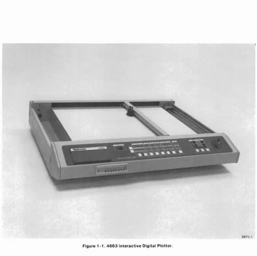
Figure 1 -1 . 4663 Interactive Digital Plotter.
2670-1
Section 1
SPECIFICATIONS
INTRODUCTION
The TEKTRONIX 4663 (and 4663S-see 4663 Opera-tor's Manual) Interactive Digital Plotter, (Figure 1-1) is capable of dual-pen graphic recording from digital source devices. The standard 4663 Plotter is equipped with a RS-232-C Communications Interface, enabling it to be used with Tektronix terminal-based systems. In addition, an optional interface is available to connect the Ploller to devices having a GPIB (IEC)' interface (such as the TEKTRONIX 4050 Series Graphic System).
The X- and Y-axes of the Plotter are controlled by split-phase synchronous ac motors (two motors in the X-axis and one motor in the Y-X-axis). These motors control the movement of a pen carriage containing two pens through a system of cables and pulleys. The internal circuitry converts external commands into appropriate vector movements. The two-pen carriage permits multi-color graphics or graphics with multiple pen types. (Note that only one pen can draw at any instant.) The pen carriage also contains a crosshair cursor, which can be used to optically check or align plolled points and for digitizing.
The 4663 will draw on a variety of media in sheets up to 17 x 22 in (431.8 x 558.8 mm).ln addition, a media advance option is available (Option 36) to automatical-ly advance a roll of paper. This option uses a 200 ft roll of paper up to 18 in wide with 1/2 in tear-off strips (containing sprocket holes) on each side. Sheet paper is held in position by electrostatic attraction generated by the platen and roll paper is held in position
mechanically by the paper advance mechanism.
I The GPIB Interlace Is defined in IEEE Standard 488-1975: IEEE Standard Olgitallnterface for Programmable Instrumentation.
The 4663 offers high quality resolution and plotting capabilities using a variety of pen types, media, and page/viewport sizes. The most basic Plotter operation is graphics - the moving of the pen carriage across the plotting surface, the lifting and lowering of either pen to produce written vectors. The Plotter can also print alphanumeric characters in any resident fonts. In addition, the Plotter can act as a digitizer, transmitting the coordinate position of the active pen along with pen status (up or down). Several user-definable variations of each recording operation can be used to increase the versatility of the Plotter. The variations include the following:
• modification of the size of the plotting area, • scaling the plots,
• manual pen positioning using the joystick, • rotation of the plot,
• alteration of the axes and character dimensions, • point digitizing,
• choice of plotting speeds and pen pressures, • use of programmable macros and,
• the initiation of a self-test.
Actual implementation of these variations differs according to the interface being used. Several user-defined variations can be conveniently introduced via a front panel Parameter Entry card. Parameters selected in this manner remain stored in the Ploller for up to 90 days, even when the PI oller is turned off.
SPECIFICATlONS
ABOUT THIS MANUAL
The service documentation for the 4663 Interactive Digital Plotter consists of two volumes. Volume 1 (this volume) contains the Plotter's specifications, preven-tive maintenance procedures (including detailed cali-bration instructions), circuit descriptions, signal de-scriptions, error codes, and a Plotter interface command summary. Volume 2 contains a short form calibration procedure, assembly/dissembly procedures for replacing parts, interconnecting cable diagrams,
electrical and mechanical parts lists, schematics, strapping tables, instrument and option installation procedures, and diagrams of circuit board component locations.
For detailed troubleshooting procedures, consult the 4663 Diagnostic Test Fixture Instruction Manual (see Section 8 of Volume 2).
GENERAL DESCRIPTION
The 4663's internal circuitry includes a 6800 and an 8X300 microprocessor. The 6800 microprocessor oversees all general aspects of the Plotter's operation. These include storing commands, communicating with the host computer, accepting front panel commands
(including Parameter Entry), etc. The 8X300 micropro-cessor, on the other hand, controls the generation of motor pen drive signals (including the pen lifters) using information supplied by the 6800 microprocessor.
SPECIFICATIONS
The remainder of this section contains a series of tables summarizing the physical properties, the elec-tronic specifications, and the performance characteris-tics of the 4663 Interactive Digital Plotter. The following tables are included:
1-2
Table 1-1 Table 1-2 Table 1-3 Table 1-4 Table 1-5 Table 1-6 Table 1-7
4663 Option Summary Accessories
Physical Characteristics Power Requirements
Environmental Specifications Performance Specifications
Page Sizes (Full Page Aspect Ratio)
Option Summary
The standard instrument contains an RS-232-C interface with Full Duplex capability. Table 1-1 lists the options which can be added to the instrument. Notice that the Plotter can be equipped with only one serial interface at a time.
Table 1 -1
4663 OPTION SUMMARY
Option Name Description
1 GPIB Provides communications with
Interface GPIB instruments, such as the TEKTRONIX 4050 Series Con-troller.
4 GPIB Same as Option 1, except that Interface the standard RS-232 interface
Only is removed.
30 RS-232 Permits the Plotter to be con-Interface nected to the TEKTRONIX to Tektronix 4081 Graphic System. 4081
31 Circular Permits the Plotter to draw Interpolation arcs and circles and to use and programmed moves and draws Program mab Ie (macros).
Macros
32 Downloadable Permits the host computer to Characters program the Plotter to draw and Math user-defined, math, and Greek Character Set characters.
36 Media Advance Permits the Plotter to be equipped with roll paper (in-stead of sheets), which can be advanced under host computer control.
37 Additional Allows more than one operat-Parameter ing configuration to be stored Entry Setup in the Plotter.
Memory
48 220 V, 50 Hz Permits the Plotter to be operated with a 220 V line source. SPECIFICATlONS Table 1-2 ACCESSORIES Standard Accessories Power Cord
Pens, Fiber Tip (for paper) Red (3 each)
Black (3 each) Blue (3 each) Green (3 each) RS-232-C Interface Cable
Sheet Paper (17 x 22 in, 100 sheets/box) 4663 Interactive Digital Plotter Operator's Manual 4663 Interactive Digital Plotter Reference Guide Optional Accessories
Wet Ink Pen Assembly
With PL3 point (dia= .01 in, 0.3 mm) PL5 point (dia= .02 in, 0.5 mm) PL8 point (dia= .03 in, 0.8 mm) Pen Replacement Parts Kit
1 cap
1 body section 1 barrel 1 locking nut 6 ink reservoirs Ink Reservoir (6 per pkg)
Ink
For Film (3/4 oz Squeeze bottle) Black (each)
Red (each) Green (each) Blue (each) Brown (each)
For Paper (3/4 oz Squeeze bottle) Black (each)
Ball Point Pens Black (3 each) Red (3 each) Green (3 each) Blue (3 each)
Fiber Tip Pens (water soluble for acetate) Black (3 each)
Brown (3 each) Red (3 each) Orange (3 each) Yellow (3 each) Green (3 each) Blue (3 each) Magneta (3 each) Purple (3 each) Dust Cover (soft vinyl) GPIB Cable
Roll Paper (18 in x 200 ft for Option 36) Sheet Paper (17 in x 22 in 100 sheets per box) Mylar (17 in x 22 in 100 sheets per box) 4663 Service Manual (two volumes) 4663 Diagnostic Test Fixture Manual
SPECIFICATlONS
Table 1-3
PHYSICAL CHARACTERISTICS
Table 1-5
ENVIRONMENTAL SPECIFICATIONS
Line Frequency 48 - 440 Hz
Input Power 115 Vac. 3.5 A maximum; 2.4 A typical
Weight Outside Dimensions
Length Width Height
80lbs 38.0 in 30.1 in 6.8 in
(36.4 kg) (965 mm) (765 mm) (173mm)
Line Voltage, Switch Selection
110V
220V
Table 1-4 POWER REQUIREMENTS
Voltage Range Line Fuse Size
90 - 130 V 5 A Fast-Blo
180 - 250 V 2.5 A Fast-Blo
Characteristic Non-operating Operating
Temperature -67to 167° F 32 to 104° F (-55 to+75° C) (0 to 40° C)
Altitude To 50,000It To 15,000It
(15240 m) (4572 m)
Vibration Upt040Hz -
-
-@01 in (.03 cm) total displacement
Shock To 30 Gs,'12sine,
-
-11 ms duration
Transportation Meets National Safe Transit Committee type of test when packaged as shipped by factory. Test procedure 1A, Category II with a 12indrop.
Humidity Mil-T-28800B per test conditions 81 OB at 50.71 procedure IV (5 day operating and non-operating, 90 to 95% Relative Humidity).
Table 1-6
PERFORMANCE SPECIFICATIONS
SPECIFICATIONS
Characteri stic Specifications
Default Paper Size A Size - 8 '12 x 11 in (216 x 279 mm) B Size - 11 x 17 in (279 x 432 mm) C Size - 17 x 22 in (432 x 559 mm) A4 Size - 8.3 x 11.7 in (210 x 297 mm) A3 Size - 11.7 x 16.5 in (297 x 420 mm) A2 Size - 16.5 x 23.4 in (420 x 594 mm) Paper Control (Sheets) Electrostatic Hold-Down
(Roll) Mechanical Hold-Down with Option 36
Paper Drive Speed :34.5 in/s (114 mm/s) (Option 36)
Paper Drive Resolution 0.016 in (0.4 mm) (Option 36)
Plotting Area Y-Axis"" 17.25 in (438 mm) X-Axis"" 23.5 in (597 mm)
-Plotting Speed 16.4 7 in/s along either axis. 23.3 in/s at a 45° angle
Acceleration 600 in/s2(15240 mm/s2)in
PREVIEW
400 in/s2 (10160 mm/s2)in
NORMAL
300 in/s2(7620mm/s2)in
ENHANCED 1
240 in/52(6096 mm/52) in
ENHANCED 2
Characteristic Specifications
Point Plotting Rate 30 Points/s (max)
Plotting Accuracy 0.15% of Vector Length± 0.0025 in (0.0635 mm)
Repeatability Returns any previously plotted point to within± 0.0025 in (0.0635 mm)
Resolution (Addressable) 0.001 in (0.0254 mm) Pen Pressure
Coarse Pressure,± 25% Pen Height (Up)
0.058 in± 0.013 (1.47± 0.33 mm) Linearity
Geometry Mean vector shall not deviate more than ± 0.015 in from a straight line between two points.
Line Aberrations Short term non-linearity shall not deviate more than ± 0.003 in from mean vector.
Orthogonality ± 0.015 in (0.38 mm) across the plotting surface.
SPECIFICATIONS
Table 1-7
PAGE SIZES (FULL PAGE ASPECT RATIO)
Page Page Size & Measurements (width x height) Figureb
Format Orientation Media Dimensions English-inch Metric-mm No.
Drafting Horizontal C 22 x 17 in 21.00x 15.5 533.4 x 393.7 1-2
Drafting Horizontal B 17 x 11 in 15.76 x 10.24 400.3 x 260.1 1-2
Drafting Horizontal A 11 x 8.5 in 10.50 x 7.74 266.7 x 196.6 1-2
Drafting Horizontal A2 594 x 420 mm 22.72 x 15.75 574.0 x 400.0 1-3
Drafting Horizontal A3 420 x 297 mm 15.75 x 10.91 400.0 x 277.0 1-3
Drafting Horizontal A4 297 x 210 mm 10.91 x 7.48 277.0 x 190.0 1-3
Drafting Vertical C 17 x 22 in 15.50 xa 393.7X a 1-2
Drafting Vertical B 11 x 17 in 10.24 x 15.76 260.1 x 400.3 1-2
Drafting Vertical A 8.5 x 11 in 7.74 x 10.50 196.6 x 266.7 1-2
Drafting Vertical A2 420 x 594 mm 15.75 xa 400.0X a 1-3
Drafting Vertical A3 297 x 420 mm 10.91 x 15.75 277.0 x 400.0 1-3
Drafting Vertical A4 210 x 297 mm 7.48 x 10.91 190.0 x 277.0 1-3
Graphing Horizontal C 22 x 17 in 20.50 x 16.00 520.7 x 406.4 1-4
Graphing Horizontal B 16.5 x 11 in 15.00 x 10.00 381.0 x 254.0 1-4
Graphing Horizontal A 11 x 8.5 in 10.00x 7.00 254.0 x 177.8 1-4
Graphing Horizontal A2 594 x 420 mm 22.20 x 15.75 564.0 x 400.0 1-5
Graphing Horizontal A3 420 x 297 mm 15.35 x 10.91 390.0 x 277.0 1-5
Graphing Horizontal A4 297 x 210 mm 10.91 x 7.28 277.0 x 185.0 1-5
Graphing Vertical C 17 x 22 in 16.00 xa 406.4X a 1-4
Graphing Vertical B 11 x 16.5 in 10.00 x 15.00 254.0 x 381.0 1-4
Graphing Vertical A 8.5 x 11 in 7.00 x 10.00 177.8 x 254.0 1-4
Graphing Vertical A2 420 x 594 mm 15.75 xa 400.0X a 1-5
Graphing Vertical A3 297 x 420 mm 10.91 x 15.35 277.0 x 390.0 1-5
Graphing Vertical A4 210 x 297 mm 7.28 x 10.91 185.0 x 277.0 1-5
aThe page dimension Is clipped since It would extend beyond the platen boundary.
bAli ligures are shown with FULL PAGE initial aspect ratio.
SPECIFICATIONS
r---.
: C AREA CLIPPED :
I I
I I
C HORIZONTAL
B HORIZONTAL
A HORIZONTAL
...J ...J ...J
<C <C <C
0 0 ~
i= l-
I-ll: ll: a:
w w w
>
>
>
0 ll:I <C
PAPER BOUNDARY
NOTE: The slight shifts of the page boundaries are due to differences in top and bottom margin widths.
For Roll Mode, the page boundaries are moved up'12".
Figure 1 -2. Horizontal and Vertical Page Orientations for English Page Sizes (Drafting).
4663 SERVICE VOL. 1
\
INDEX ARROW2669-27
SPECIFICATIONS
,---,
I
I
I
I
I
CLIPPED AREAI
I
I
I
I
I
I
1-8
A2 HORIZONTAL
A3 HORIZONTAL
...J ct
0 ...J
i= ct
a: 0
A4 HORIZONTAL
w i=
> a:
('II w
ct > ...J
M ct
ct 0
i= a: w >
'ot ct
PAPER BOUNDARY
For Roll Mode, the Page Boundaries are moved up '/2'.
Figure 1 -3. Horizontal and Vertical Page Orientations for Metric Page Sizes (Drafting),
"-MEDIA CORNERINDEX
2669-28
'\
INDEX ARROW
SPECIFICATIONS
A VERTICAL, A HORIZONTAL, B HORIZONTAL COMMON LINE
1
-I
I
I
I
I
I
I
C VERTICAL AREA CLIPPEDI
I
I
I
I
I
I
PAPER BOUNDARY
C HORIZONTAL
....
<
(,) i=B HORIZONTAL a::
w
> (,)
....
<
(,) A HORIZONTAL
i= a::
w
>
lD
....
<
B VERTICAL, (,)C VERTICAL, i=
a:: C HORIZONTAL
w
COMMON LINE >
<
~
t
Shaded Area indicates increased Margin Area.
2669-29
Figure 1-4. Horizontal and Vertical Page Orientations for English Page Sizes (Graphing).
SPECIFICATIONS
r---~
I
:
I
I
I
A2 VERTICAL AREA CLIPPEDI
I
I
I
I
I
I
A2 HORIZONTAL ...J0(
0 j:
a::
w
>
NA3
os:
HORIZONTAL
A4 HORIZONTAL
...J ...J 0(
os:
0 0
j: j:
a:: a::
w w
>
>
C')
..,
os:
os:
PAPER BOUNDARY
'"
INDEX ARROW
1-10
Shaded Area indicates increased Margin Area.
2669-30
Figure 1 -5. Horizontal and Vertical Page Orientations for Metric Page Sizes (Graphing).
PREVENTIVE MAINTENANCE
Section 2
PREVENTIVE MAINTENANCE AND CALIBRATION
NOTE
Part number 006-2398-000 is for one pad only. A box of
50
can be ordered by usinga
quantity of 50.3. The most acceptable way to clean a platen is to use water, because it will not leave a residue on the platen's surface.
4. If more extensive cleaning is necessary, use a plain detergent or alcohol pad (Tektronix PIN 006-2398-00). A plain detergent is one that contains no bleach, scents, fabric softeners, or colored crys-tals. Either detergent or alcohol pad method will leave a residue which must be removed.
General
Preventive maintenance consists of cleaning, visual inspection, adjustment, etc. Performed on a regular basis, preventive maintenance may improve the relia-bility of this instrument. The frequency and severity of the instrument's use will determine the required maintenance interval. It is, however, recommended that the Plotter's three pen drive cables be checked and adjusted at least every 500 hours of Plotter operation. Perhaps this might become the basis for performing preventive maintenance checks and calibration on the instrument. A convenient time to perform preventive maintenance is preceding calibration.
Cleaning the Platen and the Case
Occasional cleaning helps retain the electrostatic paper hold-down ability of the platen and preserves the appearance of the 4663. The frequency of cleaning varies with the instrument's environment. use the following procedure to clean the plotter:
1. Pull the Parameter Entry card out to the Media Form line and press the switch over SHEET. 2. Press the front panel MEDIA CHANGE switch. (If
the Plotter was not in SHEET mode previously, it will be necessary to press MEDIA CHANGE twice more to move the pen carriage to the upper right corner,) Then, turn the POWER switch off and disconnect the power cord. Remove any paper present on the platen.
5. If alcohol was used, remove the thin alcohol residue on the platen surface by wiping the platen with a soft, moist (with water) cloth. Turn the cloth frequently to avoid smearing the residue.
6. To remove any detergent residue, use step five, and repeat at least three times to remove all the residue.
1. Dry the platen with a clean, dry cloth.
8. Clean the Plotter case with a cloth lightly dam-pened with a mild detergent solution.
9.
Connect the power cord to the power source, and if necessary, change the Parameter Entry card's Media Form line back to ROLL mode. The Plotter may again be operated.
~
Do not use abrasive and strong chemical clean-ers on the platen, as these can scratch or remove layers of the thin insulating film on the platen's electrostatic surface. Conductive cleaners must also be avoided. These include products contain-ing ammonia, oils, liniments, or scents which leave an electrically conductive film if not entirely removed. This film causes the electrostatic paper hold-down to fail due to the conductivity of the film residue.
Viscous Oil Dampers
On the end of each pen drive motor capstan, there is a viscous oil damper. It is normal for this damper to contain an air bubble in the oil resevoir and to have a thin residue of oil on its outer surface. The damper is not defective when these items appear. The air bubble helps compensate for tolerances and heat expansion. The thin oil residue is inherently present on the surfaces of the damper, though it serves no purpose.
PREVENTIVE MAINTENANCE and CALIBRATION
Isopropyl alcohol is a partial solvent for silicone oil such as that used in these dampers. It is the only cleaning agent used to clean up oil residues. Most other solvents effective for remov-ing silicone oil will also attack the polycarbonates used in 4663 parts such as the damper covers.
~
Silicone oils have insulating properties. Do not touch circuit boards or plug connectors without first washing your handsif the dampers have been handled. Oil may prevent electrical contact or result in excess capaci-tance on circuit boards and plugs.
Lubrication Information
The Plotter requires no periodic lubrication since all cable pulley bearings, motor bearings, fan bearings, and the bearings for the Y-axis arm rollers are all permanently lubricated. In addition, the rubber treads for all Y-axis arm rollers have lubrication impregnated in them.
Pen Drive Cable Checks
The Plotter uses a system of three cables, each driven by a separate motor, to move the pen carriage.
Although the cables are coated with plastic and made of multiple strands of steel wire, they may eventually become worn and break, especially when used after extensive periods of time without adjustment. Periodically (at least every 500 hours), the entire length of the three cables should be checked for broken wire strands, kinks, worn spots, or other failures. If any of these conditions are found in a cable or its coating, replace the cable. Check and adjust the cable tension, if necessary. This procedure is covered in the instrument calibration procedures later in this section.
Introduction
ADJUSTMENT AND CALIBRATION PROCEDURES
Two X-Axis Limit Switch Calibration Fixtures (003-0840-00) .
A thorough cleaning and inspection for loose, damaged, or worn parts should precede any adjustments. It is especially important to check the three pen drive cables for broken strands, worn spots, etc., at this time. After a 30-minute warm-up period, perform the adjust-ment procedures in a +68 to+860
F(+20 to +300 C)
environment.
Equipment Required
Large screwdriver.
7/16 in nutdriver (or screwdriver listed above). Fish-weighing scales (0-6 Ibs capacity). Pozidrive screwdriver.
PBUS Extender Circuit Card 067-0813-00 (670-5235-00) .
Voltmeter (DVM). Range, 0 to
+
20 Vdc minimum; accurate within± 0.05%. Also a range to+
1000 Vdc. Short screwdriver with a narrow flat blade.5/64 in Allen wrench bent at a 900angle.
Pen Carriage Height Gauge 003-0957-00.
Pozidrive screwdriver, very short.
Y-Axis Limit Switch Calibration Fixture (003-0849-00). Oscilloscope. (A Tektronix 465 or equivalent.) Single trace with a vertical deflection factor of at least 5 mV per division and a sweep rate of at least 10 ns per division. Bandwidth should be from dc to at least 100 MHz.
C size plotting paper. Square.
Preliminary Steps
1. Turn off the power to the Plotter and disconnect the power cord.
2. Lower the two end panels by turning the large quarter-turn end panel latches'/4 turn CCW. There are two latches on each end panel (see Figure 2-1 ).
3. When both end panels have been lowered, lower the front and back panels. To do this, unscrew each of four knurled thumbscrews that hold the front and back panels in place (see Figure 2-2).
PREVENTIVE MAINTENANCE and CALIBRATION
2669-20
FRONT X-AXIS CABLE TIE-DOWN
SCREW.
FRONT OF INSTRUMENT LOOP IN CABLE
(to attach fish-weighing scale)
""
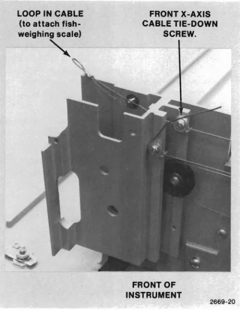
Figure 2-3. Front X-Axis Cable Tie-Down Screw and Loop Detail.
OPPOSITE PANEL IS SAME AS NEAR PANEL
/
X-Axis Cable Adjustments
TURN QUARTER TURN CCW TO OPEN (TURN QUARTER TURN CW TO CLOSE)
1. Attach a scale (like a fish-weighing scale) to a loop (you may have to tie one, preferably a Bowline) on the end of the front X-axis cable (see Figure 2-3). While loosening the cable tie-down screw next to the loop, maintain six pounds (2.7 kg) of tension in the cable.
2. Continue to maintain six pounds of cable tension while moving the Y-axis arm back and forth across the platen several times.
3. Tighten the cable tie-down screw (loosened in Step 1) while the scale continues to indicate six pounds of cable tension.
4. Repeat steps 1-3 for the rear X-axis cable (refer to Figure 2-4).
For replacement of these cables, refer to Volume 2.
LOOP IN REAR X-AXIS CABLE
LOOP IN V-AXIS CABLE
Figure 2-1. Side Panel Quarter- Turn Latches.
BACK PANEL
SWINGS DOWN
267D-4S
Figure 2-2. Front and Back Panel Thumbscrew Locations.
REAR
X-AXISCABLE nE-DOWN
SCREW
V-AXIS CABLE nE-DOWN
SCREW
REAR OF INSTRUMENT
Figure 2-4. V-Axis and Rear X-Axis Cable Tie-Down Screw and Loop Detail.
PREVENTIVE MAINTENANCE and CALIBRATION
Y-Axis Cable Adjustment
For replacement of this cable, refer to Volume 2.
1. Attach the scale, used in the previous steps, to a loop on the end of the Y-axis cable (see Figure 2-4). (Again, you may have to tie a loop, preferably a Bowline.) While loosening the Y-axis cable tie-down screw, maintain three pounds (1.4 kg) of tension in the cable.
2. Continue to maintain three pounds of cable tension while moving the pen carriage back and forth along the Y-axis arm several times.
3. Tighten the cable tie-down screw (loosened in Step 1) while the scale continues to indicate three pounds of cable tension.
Power Supply Adjustment
A.
Front of Instrument.
1. Unscrew the eight nuts (on studs) which hold the pen drive mechanism assembly to the Plotter base (Figure 2-5).
~
Before tilting up the pen drive mechanism
assem-bly in the next step, make sure the rear panel has been opened and swung down out of the way. Also, exercise care to avoid damaging or stretch-ing the pen drive cables.
2. Grasp the front of the pen drive mechanism assembly under the corner brackets and lift the front of the assembly only, back to about a 45° angle. A support rod is stored along the right side of the circuit card cage to hold this assembly up. Insert the free end of the support rod into the hole located about three inches (75 mm) to the right of the front cable capstan (see Figure 2-6).
3. Remove the circuit card holding bracket (retainer). Then, insert the PBUS Extender circuit card into any of the unoccupied circuit card cage
connectors on the right side of the circuit card cage.
2-4
B.
Rear of Instrument.
2870-48
Figure 2-5. Nuts Holding the Pen Drive Mechanism Assembly.
PEN DRIVE MECHANISM ASSEMBLY
CIRCUIT CARD ~~
CAGE
PREVENTIVE MAINTENANCE and CALIBRATION
HOLE FOR SUPPORT ROD
SUPPORT ROD (SWINGS UP)
POWER SUPPLY
. - : . _ - - - - . LINE VOLTAGE
SELECTION SWITCH
L - ~_ _.."...2669-31
Figure 2-6. Access to the Plotter's Electrical Circuitry.
4, . Plug the Plotter's power cable in and turn the POWER switch to ON. After about a five-second wait, the pen carriage moves to the upper-right corner of the platen. If the INIT light is still on, move the Parameter Entry card slightly (tully in) until the light goes out.
4663 SERVICE VOL. 1 @
5. Connect the positive lead of the digital voltmeter to Pin 71 (+12 Vdc) of the Extender card. The other lead should be connected to GND (Pin 1,2,79, or 80). Adjust R1 on the back of the power supply (use a short screwdriver with a narrow, flat blade) to obtain a
+
12 V±60 mVdc reading.6. Observe that the cooling fan is working. It is located between the circuit card cage and the power supply.
Figure 2-7. Joystick Adjustment.
PREVENTIVE MAINTENANCE and CALIBRATION
Joystick Sensitivity Adjustments
Y-Axis Adjustment
1. Insert the 5/64 in Allen wrench into the Y-axis adjustment hole shown in Figure 2-7.
2. Turn the wrench slowly until the Y-axis motor starts to turn. Note this wrench position.
3. Turn the wrench back the other direction until the :notor begins to turn the other direction. Note this wrench position also.
4. Set the final adjustment near the center of these two extreme wrench positions.
X-Axis Adjustment
1. Repeat the Y-Axis Adjustment procedure for the X-axis adjustment.
2. See Figure 2-7 for the X-axis adjustment location. This will affect both of the X-axis motors together in the same manner as for the Y-axis motor.
REAR (OR BOTTOM)
OF JOYSTICK
HOUSING
Ii
Y·AXIS ADJUSTMENT
FRONT PANEL
CIRCUIT BOARD
X-AXIS ADJUSTMENT
2669-22
X-Axis Limit Switch Adjustment
When you power up the Plotter, the pen carriage and the Y-axis arm move into the light beam of three carefully positioned photo-detectors (referred to as limit switches). These limit switches establish the initial pen position, and all subsequent plotting is done with reference to this position. Therefore, if any problems are noticed in the positioning of plots, calibrate these limit switches as follows:
1. Unplug J7, J8, and J9 from the Motor Pen Drive circuit card.
2. Connect the positive lead of the DVM to Pin 6 of the extender card (X L1M-1) and the negative lead to ground (Pin 1,2,79, or 80).
3. Attach the two X-axis limit switch calibration fixtures in place (see Figure 2-8). Both fixtures go on the right end (front and rear) of the instrument. 4. Move the Y-axis arm up against these two fixtures
as shown in Figure 2-8
5. Loosen (but do not remove) the locking screw on the underside of the front limit switch (see Figure 2-9).
6 Adjust the knurled thumbscrew to change the voltage observed on Pin 6 back and forth from a TTL high to a TTL low.
7 Tighten the locking screw on the underside of the front limit switch.
8 Repeat Steps 5-7 for the rear limit switch. This time, observe the voltage on Pin 8 of the Extender card. It may be necessary to use a short Phillips screwdriver to reach the locking screw on this limit switch.
9. Remove the X-axis limit switch calibration fix'ures.
PREVENTIVE MAINTENANCE and CALIBRATION
X-AXIS LIMIT SWITCH FRONT X-AXIS LIMIT SWITCH CALIBRATION FIXTURES
~
REAR X-AXIS LIMIT SWITCH
REAR X-AXIS LIMIT SWITCH
2669·23
Figure 2-8. X-Axis Limit Switch Calibration Fixture Placement.
PREVENTIVE MAINTENANCE and CALIBRATION
PEN CARRIAGE
2669·58
~j
~I~
~~
SECURING SCREWS
Figure 2-9A. Pen Carriage Height Adjustment.
Carriage Height Adjustment
(Plotters with serial numbers 8062075
and up)
Check the pen carriage height by using the Pen
Carriage Height Gauge Lay the gauge flat on the platen surface. Attempt to slide either end of the gauge under the pen carriage as shown in Figure 2-9A. The shaved end of the gauge should slide under the carriage easily. The thick end should not.
Y-Axis limit Switch Adjustment
Figure 2-9. X-Axis Limit Switch Detail.
2669-24
1. Attach the positive lead of the DVM to Pin 10 of the PBUS Extender circuit card.
2. Attach the Y-axis limit switch calibration fixture to the back edge of the platen (see Figure 2-10) . . 3. Move the pen carriage so that it presses firmly
against the fixture as shown in Figure 2-10. Also ensure that the fixture is seated tightly against the back edge of the platen.
4. Loosen the locking screw under the Y-axis limit switch (see the insert in Figure 2-10).Itmay be necessary to use a short Phillips screwdriver. 5 Turn the adjusting screw (see Figure 2-10) until
the observed voltage on Pi n 10 of the Extender card changes back and forth from a TTL high to a TTL low.
6. Tighten the locking screw under the limit switch (loosened in Step 4).
7. Remove the Y-axis limit switch calibration fixture 8. Reconnect J7, J8, and J9 to the Motor Pen Drive
circuit card. (These were removed in Step 1 of the X-Axis Limit Switch Adjustments.)
Figure 2-10. V-Axis Limit Switch Calibration Fixture Placement.
Raise or lower the carriage height as follows: 1, Loosen the two setscrews at each end of the
carriage (Figure 2-9A),
2, Adjust the adjustment screws in the rail adjusters until the pen carriage height is between 0.085 and 0.105 inches from the platen surface as measured with the Pen Carriage Height Gauge. The height should be checked at several locations on the platen surface,
3. When the pen carriage is set at the proper height, tighten the two setscrews in each rail adjuster to secure the adjustment screws at the proper setting.
PEN CARRIAGE AGAINST FIXTURE
2669-32
~
I V.AXIS LIMIT' - - - - SWITCH CALIBRATION
FIXTURE
PREVENTIVE MAINTENANCE and CALIBRATION
LOCKING SCREW ADJUSTING
SCREW
FIXTURE AGAINST PLATEN
V·AXIS LIMIT SWITCH
Figure 2-11. Platen Electrostatic Voltage Test Points.
Processor Timing Checks
1. Attach an oscilloscope lead to Pin 77 (MASTER CLOCK) of the Extender card. Set the oscilloscope to 10 ns/DIV and 2 V/DIV. Check that the MASTER CLOCK has a period of 67.8 ns (or 6.8 DIV on the scope).
2. Attach the oscilloscope lead to Pin 27 (INTER-RUPT TIMER) of the Extender card. Set the oscilloscope to 1 ms/DIV and 2 V/DIV. Check that the period of the INTERRUPT TIMER is 8 ms (or 8 DIV on the scope). Tolerance is± 10% or± O.Bms. 3. Turn the Plotter's power OFF.
4. Remove the Extender circuit card. 5. Replace the circuit card retainer.
6. To return the Plotter back to its normal mechanical configuration, perform Steps 1-5 of Appendix C (Volume 2) in reverse order.
2669-33
o
~PIN6
(GROUND) PIN 5
(no connection)
MOTOR PEN DRIVE BOARD
jT:~~ ~~
J11 . . . .
I-II-. .
Ifan attempt is made to measure this voltage on Pins 1-4 of J11, the input impedance of evena 10 Mil voltmeter will placeasizable load on the High Voltage Platen Power Supply. This will lower the voltmeter reading and provide an inaccurate check.
NOTE
PREVENTIVE MAINTENANCE and CALIBRATION
Measuring Platen Electrostatic Voltage
I
WARNINGt
Dangerous voltages are measured in this proce-dure. While making these measurements, make sure that you are not touching the voltmeter probe tip and that the probe tip does not touch other components or the Plotter chassis. In addition, use only one hand to hold the voltmeter probe and make sure that no part of your body is touching the Plotter chassis.
1. Place the Plotter in SHEET mode (if not already in this mode). To do this, pull the Parameter Entry card out to the Media Form line and press the switch over SHEET. Then press the MEDIA CHANGE front panel switch twice.
2. Set the voltmeter to read the
+
1000 Vdc scale. 3. Attach the negative voltmeter lead to Pin 6 ofJ11on the Motor Pen Drive circuit card (see Figure 2-11) .
4. Carefully attach or touch the positive voltmeter lead (probe) to each of the four load resistors directly behind J11 as shown in Figure 2-11. A reading of
+
880 Vdc± 10% should be measured at each resistor. The input impedance of the voltmeter will affect this reading. The technician should interpret this reading with the input im-pedance of the voltmeter in mind.Pen-To-Pen Registration Check
1. Turn the Plotter's power back ON.
2. With a pen in each pen holder (preferably each pen should have a different color) and a sheet of C size paper on the platen, press PEN SELECT 1, unless that light is already on.
3. Move the pen carriage near the middle of the platen.
4. Press the UP/DOWN switch, turning that light on. The pen carriage should move toward the rear of the instrument slightly and to the left (nearly a 45° angle). Then the pen should lower to the paper. 5. Press the UP/DOWN switch again, turning that light
off. The pen should move back to its original position, leaving a dot on the paper.
6. Press PEN SELECT 2, turning that light on and the PEN SELECT 1 light off.
7. Press the UP/DOWN switch again, turning that light on. The pen carriage should move toward the front of the instrument slightly and to the left (nearly a 45° angle) before lowering to the paper.
8. Press the UP/DOWN switch again, turning that light off. The pen should move back to its original position, leaving a dot on the paper.
9. Verify that these two dots are on top of each other.
4663 SERVICE VOL. 1
PREVENTIVE MAINTENANCE and CALIBRATION
Orthogonality Check
1. Pull the Parameter Entry card out and make the following entries:
INITIAL PAGE SIZE: C
PAGE ORIENTATION: HORIZONTAL INITIAL ASPECT RATIO: FULL PAGE AXIS ORIENTATION: Column 1
2. Press OUTLINE VIEWPORT. Remember to press the lower of the two left SHIFT switches prior to pressing the PLOT CONTROL switch. The Plotter should draw a rectangular box which has the dimensions shown in Table 1-7. Measure these to verify size accuracy and use a square to verify orthogonal ity.
Lamp Test
1. Pull the Parameter Entry card out to the EXECUTE SELF TEST line and press the switch over col-umn 2. All of the front panel lights (except the Parameter Entry light) should come on.
2. Replace any lights that are not on (see Volume 2). 3. Press the switch again to extinquish the lights.
PREVENTIVE MAINTENANCE and CALIBRATION
Line Quality and Accuracy Check
1. Press the switch over column 1 (on the EXECUTE SELF TEST line). The Plotter should draw a plot similar to that shown in Figure 2-12.
2. Examine this plot for line quality and accuracy. Early in the plot, the Plotter draws the right side of the center "X" in the box; finally, after permitting the technician to briefly exercise the joystick, the Plotter completes this center "X." Verify that the Plotter has not lost any positional accuracy by examining the center of the "X."
3. If the line quality checks indicate non-straight lines, the three dampers might be suspect. There is one damper on the end of each pen drive motor capstan, except on early model Plotters which do not use dampers. The damper is an oil-filled, inertia-absorbing device. Check to see if oil has leaked out. Notice that the damper is not entirely filled with clear-colored oil; there should be a bubble of about 1/4 to 1/3 of the damper's volume.
Joystick Operational Check
1. Move the joystick control.
2. Verify that the pen carriage moves in the direction that the joystick handle is pressed and that its speed is dependent upon the deflection angle of the joystick handle.
2-12 @
Media Advance Clutch Tension Check
1. If the Plotter is equipped with Option 36, check the paper roll clutch assembly tension. To do this, first disengage the paper from the paper drive tractors. Then, pull the paper from the roll at least six inches (150 mm) and release. The paper roll should rewind at least '12to3/4 revolution. If it does not,
refer to Appendix A of Volume 2 for the clutch adjustment (under Option 36 Installation). 2. Thread the paper back into the paper drive
tractors.
Media Advance Adjustments
1. Refer to Section 2 of the Operator's Manual for adjustments of the paper drive mechanism. There are two adjustments: one to accommodate different paper widths, and the other to adjust the paper laterally. Adjust both as necessary.
2. Turn the Plotter's power off.
This completes the adjustment and calibration procedures for the 4663 Plotter.
PREVENTIVE MAINTENANCEand CALIBRATION
Please exercise the joyst ICK
2670-11
r,-.---./
l///",
Plot ends here after Joystick use. One half of the intersection is drawn early in the plot, while the remainder of the intersection is drawn at the end to verify repeatability.
Figure 2-1 2. Test Pattern Produced by Self- Test Feature.
SYSTEM DESCRIPTION
THEORY OF OPERATION
Section 3
icates primarily with the Vector Generator. Physically, however, the Motor Pen Drive circuit card connects into the backplane to obtain its power. Figure 3-1 shows the functional piggy-back relationships.
The 4663 Plotter contains two microprocessors. The 6800 residing on the Processor circuit card controls the overall operation of the Plotter. The second micro-processor (an 8X300) resides on and controls the operation of the Vector Generator functional block. The Plotter is electrically organized such that the 6800 microprocessor views all other functional blocks as peripheral devices, including the Vector Generator and its microprocessor.
The basic electronics structure of the 4663 Plotter is composed of functional blocks residing on a central bus. A diagram of this structure is shown in Figure 3-1. The central bus is an 80-pin backplane circuit card cage and most functional blocks, representing circuit cards, connect directly into this backplane. There are a few exceptions, however, where a functional block does not connect directly to the bus. First, the Parame-ter Entry, Front Panel Switches and Lights, and the ROM Patch blocks "piggy-back" onto other modules, which in turn, are connected to the central bus. Second, the Motor Pen Drive block is functionally piggy-backed, or indirectly connected, to the Vector Generator module, simply because this block
PROCESSOR/ MEMORY ECB
BACK PLANE COMMUNICATIONS
MC 6812H21 INTERFACE ECB
MICROPROCESSOR
... GPIB
...
BUS
...
...
I/OCONTROLLER
"
...
(ROM)...
SERIAL
RAM
...
...
...DrY
I/OQ
...
"
ROM ...ROM
~
FRONT PANEL LIGHTS
AND SWITCHES
X-AXIS MOTOR
X-AXIS MOTOR HOST
t
...
INTERFACE.,
ADAPTER... RS232
"
ADAPTERTEtM MOtEM
t+---l~ JOYS TIC K BIPOLAR
PROCESSOR ROM RAM
I/O
...
...
"
DMA... FRONT PANEL I/"'~----~ ... ., CONTROLLER ...
f - - - i VECTOR GENERATOR
DMA CONTROLLER PRODUCT
BUS (PBUS)
"I ,.
~
...
00
¢
MOTORPEN ~DRIVE
00
...
L
PARAMETER ENTRY MISC.I/O
PARAMETER ENTRYI v - - - ' / I I/O
,'--- ROM PATCH ' - - - DIAGNOSTICS
I
SENSOR:
F=
ADVANCEMEDIA IV----"I'J(OPT! ONALl ...
MEDIA
TRACTOR
0
MOTOR
THEORY OF OPERATION
POWER
SUPPL YI - - - i - . l
PEN SOLENOIDS
AXIS LIMIT SENSORS
2669-34A
Figure 3-1. Functional Block Diagram of the 4663 Plotter.
THEORY OF OPERATION
BACKPLANE (CENTRAL BUS)
CIRCUIT CARD EJECTOR
NOTE
The right and left sides of the Backplane areNOT
symmetrical. Therefore, itisnot possible to interchange circuit cards from the left side to the right side and vice-versa. However, itispossible to interchange any of the cards within a side.
A detailed description of the electrical signals on the Backplane is located in Appendix A of this volume. A pin/signal list is included in Volume 2.
MOTOR PEN DRIVE
MEDIA ADVANCE (OPT. 36) INTERFACE (serial)
CIRCUIT CARD CAGE (front view)
The 4663 Backplane is a circuit board with eight 80-pin connectors, each of which is designed to connect to a circuit card. This arrangement forms a bus
structure between the other functional blocks. On most cases, each functional block represents one circuit card.) A diagram of the 4663 Backplane and the functional blocks that connect directly to the Backplane are shown in Figure 3-2.
PROCESSOR VECTOR GENERATOR
3453-50
Figure 3-2. 4663 Backplane.
THEORY OF OPERATION
INTER-FUNCTIONAL BLOCK COMMUNICATIONS PROTOCOL
STROBE (ASTB-O), also sent from the Processor. One bus clock cycle later, at 2, the address value has settled and can be considered valid. Notice that the WRITE-O control line is not asserted with the address in this example; this indicates a Read transaction is occurring. Several bus clock cycles (at a frequency of 14.7456 MHz) later, at 3, the device being read (a RAM, ROM, or I/O register) places BUS DATA on the lines BDO-1 to BD15-1. BUS DATA is simultaneously quali-fied as valid by DATA STROBE (DSTB-O), which is also sent from the device being read. One bus cycle later, at 4, the data value has settled and can be considered valid.
The delay between address assertion by the Processor and data response by the device being read is the device access time; it may range from one bus clock cycle (67.8 ns) up to when the total read transaction is completed (within 3.8 /As, which is the bus timeout period). The assertion of ASTB-O must precede
DSTB-o
by at least one bus clock cycle. If DSTB-O is not asserted before the bus timeout period, the Processor assumes the device being read is non-existent and automatically terminates the transaction by releasingI
I
I
BA"-1
~
:
:>
BUS ADDRESS TO
6A15-1
- I
I
AOORESS STROBE ASTB-"~
I
Iff
I
I
II
I.ok'
ADDRESS VAL IO:>
60"-1
-I
k
BUS DATA TO
I B015-1
-~
~
I
DevIce beIng re.dI
DATA STROBE DSTB-"
---7$
I
V/
PROCESSO~
I
I
I
r.-
DATA VALIDI
I
WRITE-"
I
I
I
I
I
(NOTII ThIs
Is h1Shl I I I I I
CD
®
@
0
®
®
I
ASSERTI
RESPONDI
OPTIONALI
RELEASEI
RELEASEI
ADDRESS WITH RECEIVER DATA DATA
I
CO~~OL
I
DATAI
TRANSACTIONI
STROBEI
AD~~~SSI
HOLD
ADDRESS CONTROL
BEGIN VALID END
TRANSACTION TRANSACTION
~ 87.BNS ~
BCK-l
For the purposes of this manual, "Processor" refers to the main Plotter microprocessor (i.e., the 6800).
NOTE
The rest of this section gives detailed circuit descrip-tions.
Following is a description of the communications protocol between the functional blocks in the 4663. The basic transactions are the following:
Read Write Interrupts
DMA (Direct Memory Access) I/O Addressing On/Out)
Read Cycle Description
The Read transaction begins when the Processor places the BUS ADDRESS on lines BAO-1 to BA 15-1. (This is labeled as 1 in Figure 3-3.) The address is simultaneously qualified as valid by ADDRESS
Figure 3-3. Bus Read Transaction Timing.
both BUS ADDRESS and ASTB-O. The Bus Control causes the BUS TIMEOUT INTERRUPT to be generated to the Processor whenever the bus timeout period has been exceeded.
One clock cycle after the device being read has asserted DSTB-O (at 3), the device releases it (at 4, when data is defined as valid). If the Processor requires a longer hold time for the data, it must now assert DSTB-O. This ensures that the Processor has control of the transaction and can delay the termination if necessary. At 5, the Processor releases DSTB-O, indicating that it has read the BUS DATA. Finally, one bus clock cycle later, at 6, the Processor releases BUS ADDRESS and ASTB-O, which also causes the device being read to release BUS DATA. This completes the entire Read transaction. On the next falling edge of the bus clock, a new transaction can begin with the assertion of a new BUS ADDRESS by the Processor.
Write Cycle Description
The Write transaction begins when the Processor places the BUS ADDRESS on the lines BAO-1 to BA 15-1. (This is labeled 1 in Figure 3-4.) The address is simultaneously qualified as valid by ADDRESS
~ l!l7.l!lNS ~
THEORY OF OPERATION
STROBE (ASTB-O), which is also sent from the Proces-sor. One bus clock cycle later, at 2, the address value has settled and can be considered valid. Notice that the WRITE-O control line is also asserted with the address in this example. This indicates that a Write transaction is occurring. Several bus clock cycles later, at 3, the Processor places BUS DATA on the lines BDO-1 to BDBDO-15-BDO-1. The BUS DATA can be considered valid one bus clock cycle later, at 4, when the data value has settled. The delay between address assertion by the Processor and data assertion may range from one bus clock cycle up to when the total write transaction is completed (within 3.8ILs,which is the bus timeout period). The assertion of ASTB-O must precede
DSTB-o
by at least one bus clock cycle.All information is now valid, and at 4 the Processor releases DSTB-O, since it was held for one bus clock cycle. The device being written to must now assert DSTB-O for a minimum of one bus clock cycle until at least 5. If the device being written to requires a longer hold time for the data, it must continue to hold DSTB-O. This ensures that the device has control of the
transaction and can delay the termination, if necessary (in case the device has a slower memory, for example). If the device does not hold DSTB-O, the Processor assumes that the device being written to is
non-BCK-l WRITE-0 BUS ADDRESS ADDRESS STROBE eus DATA DATA STROBE BA0-1 TO BA15-1 ASTB-0 BDIIl-l TO 15015-1 DSTB-1Il I 1
~--+---
--:...
- ---_---+---1
~
I 1- I
~
1---1---1----.1
I I ADDRESS V_A-L-ID--I---_~--___l_---_I..
I
1
1<...
- 1 - - - - 1 - - - - 1 - - - 4 '___1~!~7C7ES~S~O_R_~ _
I I I
//OEVICE BEING I
WRITTEN TO
~
: :~
DATA J A L I D VI: '\.\"'--+-1--+1- - + - 1- - + - 1
- - + - - - - /
m
®
@
@
®
@
0
IADDRESSASSERT I ASSERT IRECEIVER RECEIVERIOPTI ONAL1RELEASE I RELEASEDATA DATA 1 ICONTROLAND IADDRESSDATA IACKNOWL-ITRAHSACTIONI STRoeEEDGE HOLD I ADDRESSCO~~~OL
I
BEGIN VALID END
TRANSACTION TRANSACTION
2669-41
Figure 3-4. Bus Write Transaction Timing.
THEORY OF OPERATION
existent and automatically terminates the transaction by releasing both BUS ADDRESS and ASTB-O. The Bus Control causes the BUS TIMEOUT INTERRUPT to be generated to the Processor if the bus timeout period has been exceeded. This might occur, for example, if a memory location has failed.
When the device being written to has stored the BUS DATA, it releases DSTB-O, at 6. This signals the Processor to end the write cycle. On the next bus clock cycle, at 7, the Processor releases BUS ADDRESS, ASTB-O, WRITE-O, and BUS DATA. Then, on the next falling edge of the bus clock, a new transaction can begin when the Processor asserts a new BUS AD-DRESS.
Interrupt Operation
The Plotter is an interrupt-driven device. This means that each module has a predetermined interrupt level visible to the 6800 Processor. Before a functional block receives or generates some activity, it must first
interrupt the Processor. The Processor completes its present activity and then services the interrupt, unless a higher priority interrupt comes along. The interrupt is serviced according to a set of instructions stored in ROM (the system firmware). This means that if a functional block generates (or transmits) a request for action to another block(s), it must first convert the request (or data) into an 8-bit data byte(s) before interrupting the Processor. Some typical requests that generate interrupts include pressing a front panel switch, host-generated commands, joystick commands, generating output responses to the communications interface, turning the front panel lights on or off, etc.
The Plotter uses eight levels of priority-vectored inter-rupts to identify the functional block requesting the interrupt. The Processor can then access the system firmware for instructions on servicing that interrupt, since each interrupt level has its own interupt vector in the system firmware (ROM).
3-6
eN
The eight levels of priority interrupt are used with a serial poll scheme, which is controlled with a three-bit counter (Interrupt Poll Counter, located on the
Processor circuit card). This counter runs continuously on the bus at one-half the bus clock frequency (or 7.3728 MHz). The three counter lines are INTERRUPT POLL 0-1 to INTERRUPT POLL 2-1 (IRPO-1 to IRP2-1). When a functional block with a pending interrupt sees its preassigned (strapped) interrupt level appear, it asserts INTERRUPT REQUEST (IRQ-O). This signals the Processor to begin its interrupt sequence. If, however, the Processor is busy at that time and can not immediately service the interrupt, the Interrupt Poll Counter continues to count. However, the limits of the count are modified to eliminate counts of a lower priority. This means that the counter counts only between 0 (the highest priority) and the level of the pending interrupt, but no lower. Each time the counter counts to a lower priority level, the functional block with a pending interrupt drops the IRQ-O signal. The poll count therefore continues, scanning only for higher priority interrupt levels. When the Processor finishes its present activity and reaches the vectoring stage of the interrupt cycle, the current pending interrupt having the highest count is used to locate the next interrupt vector.
A higher level (priority) interrupt, if one occurs before the Processor's vectoring in the interrupt sequence has started, may subsequently update a lower priority limit. This means that a functional block with a higher interrupt level can come along and also assert IRQ-O when it sees its strapped interrupt poll count. Then, all subsequent poll counts wilt be between the highest priority and the new interrupting device's level. There-fore, the device with the first interrupt will not be included in the poll count. After the Processor has serviced the highest priority interrupt, the poll will expand again to include the lower priority levels (or down to the next highest priority level with a pending interrupt). This expansion occurs when the interrupt service firmware handler writes a new interrupt control byte to the interrupt poll hardware.
A table of the plotter's assigned interrupt levels is shown in Appendix E of Volume 2.
A timing diagram of the interrupting process is shown in Figure 3-5; the following discussion explains the key points in this diagram.
The INTERRUPT REQUEST POLL (IRPO-1 to IRP2-1) occurs synchronously with bus clock (but at one-half the frequency) but asynchronously with any bus trans-actions, (shown by 1). A level 2 module with a pending interrupt sees the level 2 poll count at 2 and asserts INTERRUPT REQUEST (IRQ-D). This action now estab-lishes the lower priority limit at 2, resets the poll counter, and initiates the Processor's interrupt service cycle.
The interrupt request poll continues over the range 0-2. Notice that whenever the poll count is anything but 2, the level 2 interrupting device releases IRQ-D. Then, before the Processor can clear the level 2 interrupt, a level 1 module with a pending interrupt appears, at 3. This level 1 interrupting device sees the level 1 poll count appear and asserts an INTERRUPT REQUEST (IRQ-D), which establishes 1 as the new lower priority level at 4.
THEORYOF OPERATION
With two interrupts now pending, the Processor finishes the current transaction while the poll contin-ues to count within the new limits 0-1. After the Processor has completed the prior transaction and the poll counter has counted to the level number of the interrupting module (in this case 1), the Processor locates the interrupting vector and transfers to the appropriate service routine in system firmware to clear the interrupt at 5. Since the poll counter is now limited to level 0 and 1 interrupts, the pending level 2 interrupt must wait until the Processor is finished with higher priority transactions. After the level 1 interrupt is cleared, the poll counter is allowed to count again until it reaches the next highest priority interrupt level (which is now level 2) at 6.
The level 2 interrupt establishes the upper scan register at 2 and initiates another interrupt cycle by asserting IRQ-O, and the process is repeated until this interrupt is also cleared. Then, with no other interrupts pending, the interrupt poll counter proceeds to count between 0 and 7, waiting for another interrupt from one of the 4663 functional blocks.
BCK-l
1 I
I
I1
I
I
IIRPI!l-l
X
X
X
XJ][)(
X
X
2X
I2lTO
::](
,
X
2 I2l I2l I2lIRP2-1
1 1 1 1 I 1
1 1 1 1
I
1~JII
~~\~~~\
If.
IRQ-Ill I
~~\\\,
Iffff
~\\\\\
$fff$
I
I I 1 1 I 1
I
I
1 1I
1I"
II
ON LEVEL 2 DEVICEINTERRUPT PENDING 1I
I
1 1 11 I" INTERRUPT PENDING ~I 1
1 ON LEVEL ,1DEVICE
I 1 1 1
1 I 1 I.. ~I I" ~
1 I 1 IIPROCESSOR INTERRUPTSERVICE CYCLE IPROCESSOR INTERRUPTSERVICE CYCLE
1
I
1 FOR LEVEL 1 DEVICE IFOR LEVEL 2 DEVICECD
®
@@
®
®
2669-42
Figure 3-5. Bus Interrupt Timing Diagram.
THEORY OF OPERATION
Bus DMA Operation
In the interest of speed, the Vector Generator through its DMA (Direct Memory Access) Control receives all of its data from the "circular queue:' a 64-byte portion of the main system RAM. The DMA Bus Control in the Processor module transfers data to the Vector Genera-tor's DMA Control during the Processor's Phase 1 clock time (when the Processor is inactive). (Phase 1 and Phase 2 descriptions are given later in the Processor circuit descriptions.) The DMA Bus Control transfers the data one character at a time. Once the Vector Generator DMA has received the data, the 8X300 Processor can read it to compute a subsequent Move or Draw. During Phase 2, the 6800 resumes its normal activity. On the following Phase 1, the two DMA ports can transfer another character from the circular queue. So, the main Processor operates during Phase 2, and the Vector Generator gets its data during Phase 1. Once a move or draw vector is computed, the Vector Generator generates pen drive motor signals. The Motor Pen Drive circuit card uses these signals to produce currents and voltages for the three pen drive motors and the two pen solenoids.
The structure of the bus is such that there is a single master Processor (the 6800) and up to eight DMA (Direct Memory Access) devices. However, in reality, only one DMA device is actually present. This is the 8X300 microprocessor in the Vector Generator module. The DMA scheme uses a 3-bit counter, the Bus
Request Poll Counter, which is similar to the Interrupt Poll Counter described previously. The Bus Request Counter runs continuously on the bus at one-half the bus clock frequency (7.3728 MHz). The three lines used by this counter are BUS REQUEST POLL (BRPO-1, BRP1-(BRPO-1, and BRP2-1).
A DMA operation can take place anytime that the bus is free (for example, during the Processor's Phase 1 clock cycles). First, the Vector Generator DMA Control as-serts BUS REQUEST (BRQ-O) when it sees its address (001) on the BUS REQUEST POLL lines. However, unlike the Interrupt Poll Counter, BRQ-O halts the Bus Request Poll count at 1. After the Processor has completed its present transaction, and Phase 1 has started, the Processor's DMA control asserts BUS GRANT (BGRNT-O) on the first falling edge of bus clock. This indicates that the bus is free and the Vector Generator's DMA Control may use the bus for one character transfer.
3-8
BCK-l
1
I
1 BaRNT-tI I
1\
I
(BUS GRANTl - 1
I
1ASTB-tI
~
n
(ADORESS
I
HI
STROBEl
I
I
I
1BRP9-1TO
=*6
I
:
:
BRP2-1
X7
X
eX
X[
(BUS REQlEST
I
POLLl
I
I
I
BRQ-8
I
•
I
11/
(BUS REQlEST)
I
II
I
I 1 11 ~8X38I1J PROCESSOR REQlESTED BUS ACCESS
I
1
I
I
I
I
~I~ SINGLE CHARACTER---.\
I~ PROCESSOR TRANSFER
OHA TRANSFER
I 1
CD
®
@
@
2669-43
Figure 3-6. Bus Character DMA Timing Diagram.