-THE CENTRAL COMPUTER
OF THE UNIVAC SYSTEM
MANUAL OF OPERATION FOR
UNIVAC SYSTEM
--~. -- - - - -~--.
MANUAL OF OPERATION FOR UNIVAC SYSTEM
Table of Contents
CHAPTER TITLE
-
PAGEI Description of UNIVAC and 1
Introduction to Programming
II Introduction to Computer 13
Operation
III Introduction to UNIVAC Logic 57
IV Input-Output Orders 67
V Supervisory Control and 78
Checking Circuits
VI Manual Operating Procedures 95
PREFACE
The purpose of this manual is to serve as a reference text for personnel learning operational procedures of the UNIVAC System. It was not intended as an encyclopedl c reference to the System, and in actuality provides operational information for the central computer only. No prior knowledge of UNIVAC or other large scale digital computers is presumed.
The first four chapters provide a general introduction to the central computer and may be of interest to readers other than operators. The elements of pro-gramming, logical design, and the order code are described. Since the logical design of the UNIVAC is exceedingly complex it would be quite outside the
scope of this manual. A knowledge of logic is essential to meaningful under-standing of the operation of the computer however, and is the reason for describing a Simple computer in Chapter II. The elements of UNIVAC are then introduced by analogy with the components of the Simpler computer.
The final three chapters comprise a description of the Supervisory Control Console and normal and error diagnostic procedures. Only the more cOlllllon
SECTIOO I
CHAPTER I
DESCRIPTlOO OF UNIVAC AND INTR(l)UCTlaJ TO PROGRAMMING
Concepts of a Computer
The UNIVAC is a large electronic device designed to perform repetitive cler-ical or mathematcler-ical operations at a high rate of speed and accuracy. In order to make clear the function of each component of the computer and its relationship to other components, let us consider the operation of a payroll clerk.
The clerk has a stack of time cards showing the number of hours a company's employees have worked during the week. She has a second stack of cards which show for each employee certain bits of fundamental information such as the hourly rate of pay, dependents, etc. As a work aid she uses a calculating machine which performs addition, subtraction, and multiplication for her.
In addition, she herself provides a factor of control or procedure, she se-lects the time card and hourly rate card for a particular employee. By means of the calculator she computes the man's gross pay, subtracts his income tax, old age insurance tax, etc., and ends up with the man's net pay which she enters in her ledger book.
This payroll process can be thought of in terms of four basic operationsa Input, Output, Arithmetic, and Supervision. As shown in figure 1, the time cards and hourly rate cards are the input data, the calculator is the arith-metic unit, and the output is the net pay entered in the ledger. The whole operation is supervised and executed by the clerk.
If we think a bit more about the position of the clerk in this process, we recognize that her ability to turn the input of time cards and hourly rate cards into the ledger entries of net pay depends upon her remembering the in-dividual steps of the operation -- the rules; that is, she must remember that she is to subtract the income tax from the gross pay, and that the income tax is computed by multiplying the number of dependents by $600 and so forth. Her
supervision then actually consists of memorizing the necessary steps and~
trolling the order of their execution. This memory function becomes more ap-parent if the clerk has other duties to perform as well. For instance, she may be expected to maintain the hourly rate cards, adding or removing depend-ents upon notice, or changing the hourly rate when a man is given a raise.
z
o
-<I>
-
\-::>
The UNIVAC is such a General Purpose Computer. Its five components and their interrelations are shown in figure 2. The memory occupies a central position. It holds for processing the information which has been read by the input ~e
vice. It also holds the instructions that tell what to do with this input in-formation. The control unit selects each instruction from the memory and ex-ecutes it.
An
instruction might call for the hourly rate and total hours worked to be sent to the arithmetic unit for multiplication, and return the product to the memory. As the net wages are computed, they are sent to the output device for permanent recording.In order to secure high operating speeds these five components are of electronic construction, and to assure complete accuracy many of the units are duplicated and cross checked. There are other checking methods used when it is not fea-sible to duplicate equipment.
There is yet another method of categorizing computers which is intimately related to the concept of memory. The basic element being processed by a com-puter is ~ number. We are all familiar with two methods of representing num-bers.
1) The digital method, probably the oldest, uses a special symbol or mark to represent each number. For example, we use the Arabic symbols with the posi-tion concept when we indicate that a dozen is "12" and a dozen dozen,gross,is "144".
2) The analog method is familiar to us in the slide rule, where numbers are represented by different distances along a stick.
An
ammeter represents the number of amperes of current flow by the angle of a pointer. Other commonly used representations are electric current flow, rotation of a gear or shaft, and extension of a spring.Computers may then be of two general types, special purpose or general purpose, depending on whether or not they have a stored program of instructions. Within each type a computer may be digital or analog depending upon the manner of re-presenting numbers.
The UNIVAC is a General Purpose Digital Computer. SECTIaJ 2
Organization of UNIVAC Memory
To understand the operation of the UNIVAC we start with the central element of the five, the memory. Delaying until later a description of the physical make-up of the memory, we will describe its general characteristics as concern the user of the computer. The basic unit of memory in the UNIVAC is the "word". A word always consists of twelve characters or digits. There are 63 characters available; any combination of twelve of these constitutes a word. The 63
CONTROL
UNIT
to
,
INPUT
DEVICE
~MEMORY
OUTPUT
~ ~
,
DEVICE
•
,
012345678906 -00125000000 ABCDEFG986KL JOHNNY-JONES
The main memory of UNIVAC has the capacity to "store" or "remembeI" 1000 such words. The memory may be visualized by thinking of 1000 boxes and in each box is a slip of paper with a UNIVAC word written on it (figure 3). In order to locate a particular word, we number or Ii address" the boxes. In UNIVAC the boxes are numbered consecutively from 000 to 999. Thus we can speak of the word in box 001 as being Johnny-Jones.
Earlier we mentioned that a General Purpose Computer stores the procedure or program it is to, follow in the memory. The program consists of a number of elementary operations which are combined in ~uch
a
way as to produce the de-sired anSwer. These elementary operations are called instructions. There are43 different instructions to which the UNIVAC will respond. Each instruction requires six characters for its speCification, for example:
BOO 934
The six characters are designated from left to right as "first instruction digit", "second instruction digit", "third instruction digit", ••• "sixth in-struction digit". Generally, the fourth, fifth, and sixth inin-struction digits are the address of a particular box or memory cell, and the first and second instruction digits tell what operation is to be performed on the word in that cell. The third instruction digit plays no part in the operation of the in-struction. Since each instruction consists of six characters, a UNIVAC word can consist of two instructions. The six characters on the left-hand side of a word are called the left instruction, and the right-hand six are called the right instruction.
In addition to the 10OO-word main memory there are some special memory regis-ters. These registers may be divided into three groups: 1) Arithmetic Regis-ters, 2) Control Registers and 3) Transfer Registers.
Arithmetic Registers
Control Registers
Transfer Registers
{Register A, rA, which holds one word Register x, rX,
"
"
"
"
Register L, rL, ""
"
" Register F, rF,"
"
"
"
{contrOl Counter,
ce,
a one-word register Control Register, CR,""
""
Static Register, SR, " half-word register
{
Register V, Register Y,
Register I, Register 0,
rV,
rY,
rI, rO,
t-o..
UJ
( J Z
o >
( J a:::
o
...J % C( l&J
;:) %
en
- ( J
> C(
>
c _
UJ z
-
;:)~ - La.. ...J 0 0..
%
SECTIa.J 3 Mode of Qperation
The basic principle of operation of a General Purpose Computer, that is, a computer whose operating instructions or program are stored in the memory, consists of two general parts: a) Locate the instruction to be executed, and b) Execute it.
In UNIVAC, the Control Counter, a one-word register, contains the address (i.e. location) of the next instruction word. The three address digits are on the extreme rights OOOOOOOOOXXX, the XiS stand for any number between 000 and 999. Since each word may hold two instructions, each look-up in the memory extracts two instructions.
The basic cycle of operation in UNIVAC consists of four stages. Each stage is assigned a letter of the Greek alphabet to identify it. The four-stage cycle is executed in the order:
Stage 0( (Stage I)
(.3
(Stage 2)o
(Stage 3)<i) (Stage 4)
This cycle then repeats itself.
Description
Send the right-hand six digits of the word in the Control Counter to the Static Reg-ister.
Extract the word from the memory location specified by the right-hand three digits in the Static Register and place it in the Control Register, CR.
Send the word in the Control Counter to the adder, add one to it, and return the sum to CC.
Send the left-hand six digits of the word in the Control Register to the Static Reg-ister and, treating it as an instruction, execute it.
Send the right-hand six digits of the word in CR to SR and execute it as an instruct-ion.
As can be seen, if the Control Counter initially reads 000000000000 the in-structions will be executed sequentially, first the left-hand instruction in cell 000, then the right-hand one. The next instruction is the left-hand one in cell 001, then the right-hand one in that cell, then the left-hand one in 002, .etc.
Register can hold only half a word, the Control Register is required to store the right-hand instruction while the left one is being executed. The operating speed of a computer is largely governed by the amount of memory look-up; thus, by having a Control Register we need only one look-up to select two instruc-tions.
SECTI~ 4
Elementary UNIVAC Instructions
At this point it will be helpful to introduce som~ basic instruction prders) and prepare a few sample problems. This will tie together the foregoing concepts. Generally speaking each of the 43 UNIVAC instructions can be thought of as belonging to one of three groups:
A) Instructions which transfer information from one memory location to another or from one media to another.
B) Instructions which perform the arithmetic operations of addition, subtraction, multiplication and division.
C) Instructions which allow a choice between fQllowing one of two se-quences of instructions.
Most of the UNIVAC instructions are redundant. That is, many of the instruct-ions can be done by combinatinstruct-ions of other instructinstruct-ions. The particular in-structions for the UNIVAC were selected after studying many applications to determine which would most enhance the operating speed. Under Group A we will make use of the three instructions B m, C m, and L m.
B m instruction: This instruction when it is in the Static Register* causes the UNIVAC to extract the word in memory cell m and place it in rA and rX, wipi~g out the previous contents of those two registers. The word will still be present in memory cell m. This last statement is true for all UNIVAC orders which transfer information out of the main memory.
As an aid in memorizing the code it will be noted that the orders are of mnemonic character. Thus liB rrt' can be read as "Bring the contents of memory location minto rA and rX."
The complete six digit appearance of the B m instruction is: BOOXXX where the, X's refer to some memory location between 000 and 999. Some, but not all, in-structions require specification of the second instruction digit. Those that do not usually have a zero in this digit position. No instruction requires specification of the third instruction digit and this position usually is
written as zero also. To save effort in writing the instructions, these digits are usually omitted when they needn't be specified.
L m instruction: This is very similar to B m. It causes UNIVAC to transfer the word in memory location m to rL and rX, erasing the previous contents of those two registers.
Reg-C m instruction: In executing this instruction the UNIVAReg-C erases the contents of memory location m and places in this location the contents of rAe After the transfer, the contents of rA are replaced with decimal zeros.
The only instruction in group B we shall consider at this time is the A m.
6
m instruction: This is executed in two steps:1) The word in memory location m is transferred to rX, the previous con-tents of rX being erased.
2) Then the contents of rA, and rX are sent to the algebraic adder, ad-ded, and the sum returned to rAe
The additio~ in step 2 is algebraic. The signs of the two numbers being in the left-most digit positions. For example, the proper sum of 012345 678905* and -01 III III III is 001 234 567 794. Also any alphabetic character is passed on to the sum unchanged:
012 456 014 892 032 A69 Cll 54G
044 1(25 CZ6 43G
AOO 006 COO 125 007 BO;3 198 OOZ A07 809 C98 l2Z Among the group C instructions are the
00 m instruction: This requires a zero as the second instruction digit. This is the skip order. It tells UNIVAC to pass directly to the next instruction without altering any registers or memory cells. Address m is ignored.
9 m instruction: This is the stop order. It causes UNIVAC to stop executing instructions, leaving the registers and memory unaltered.
U m instruction: The orders previously discussed could be performed as either right- or left-hand instructions. This is true for all UNIVAC instructions except the U m, Q m, and T m orders. These should be right-hand instructions to perform properly. U m is an unconditional transfer of control instruction.
It tells the UNIVAC to erase the three right-hand digits of the word in the Control Counter (the address of the next instruction pair.) and put in their place the three digits of the memory location part of the U order. That is, if the order is UOO 325 and the Control Counter contains 000 000 000 114, the "114" is erased and replaced by the "325". This and the Q order below are two means of breaking the sequential execution of orders.
Q m instruction: This is a conditional transfer of control. If the contents of rA and rL are identical the Q instruction is interpreted as a U order. That is, if (rA)-(rL)** the memory address digits m replace the address digits in the Control Counter. If (rA)~(rL) the Q m is interpreted as a skip.
SECTICN 5 Simple Problems
As our beginning problem in simple coding, let us assume that memory location 100 contains a quantity A and memory location 101 contains a quantity B. Let us design a program that permits the computer to interchange A and B and then stops the computer. We shall start our program in memory location 000 for convenience. Let us also not concern ourselves as to how the program is placed
in the memory, but assume instead that everything we need will be placed in the cells indicated.
Memory Cell Left Instruction Right Instruction
000 BOO 100
coo
102001 BOO 101 COO 100
002 BOO 102 COO 101
003 900 000 000 000
This program is elementary, yet it shows how the instructions are strung to-gether to obtain the desired results. Here a temporary storage place for the contents of cell 100 (A) are needed while we place B, the word in 101, in cell 100. Then we can take A out of temporary storage and place it in cell 101. All we need do to execute the program is to start the computer on ex time with 000 000 000 000 in the Control Counter.
A more advanced program is the following: memory cells 100 - 999 contain a set of numbers. We wish to add these 900 numbers together, place the sum in memory location 099 and stop the computer. Here the numbers to be added are deliberately chosen to be too large to be written out in detail, that is, to code 899 additions. A method of doing the problem is illustrated in the fol-lowing program: (The left-hand instruction and right-hand instruction are staggered to allow space for explanatory remarks.)
Memory Cell L H I R H I Remarks
000 COO 099
COO 099 Zeros 099
001 BOO 099
AOO 100 Add first number to 099
002 COO 099
BOO 001
003 LOO 007 Go to cell 006 if the number in QOO 006 cell 999 has been added
004 AOO 008
COO 001 Increase the instruction in cell 001 to add the next number
005 000 000
UOO 001
006 900 000 stop the computer
000 000
007 BOO 099
AOO 999
This example illustrates an important concept of programming, the iterative routine. Initially we place zeros in cell 099 and then put down the instruct-ions necessary to add the first of our 900 numbers. Next we alter these in-structions so that they will be able to add the second number to the partial sum. Then by repeating the addition process we will have added the second number, then the third, and so forth. In order to stop the computer we must know when the last number has been added. We will have added this last number when cell 001 contains the instruction BOO 099 AOO 999.
By examining cell 001 after adding a number to the partial sum we can stop when the last number has been added.
This problem illustrates one of the most useful characteristics of a stored program computer - the ability to subject its instructions to the same arith-metic operations as it does its data, that is, the power to alter its instruct-ions.
SECTION 1
CHAPTER 11
INTRODUCTION TO COMPUTER OPi:RATIONS
Preliminary Discussion
The purpose of this Chapter is to present information which will lead to an understanding of the fundamental operation of UNIVAC. It should be clear that the scope of this development will be on an elementary level. In pursuance of this idea it is planned to discuss in some detail a simple computer which uses components contained in UNIVAC, but, it must be emphasized, this computer will not be UNIVAC. The following chapter will point out the similarities and differences that exist between UNIVAC and the computer herein developed. However, before describing the computer and its relationship to the operation of UNIVAC, it is advisable to review some elementry concepts of electricity.
SECTION 2
~ Electrical Concepts
,--_ _ B_A_T_T_E_R_y-l
~_S_W_IT_C_H
_ _ _ _ _ ---..R
A B
FIG. 1 VOLTMETER
The simplest form of electrical circuit is a battery with a resistance con-nected to its terminals as shown in Fig. 1. A complete circuit must have an unbroken path so that current ~an flow out of the battery, througn the elements connected to it and back into the battery. The circuit is broken or opened if some part of this path is removed. A switch is a device for opening or closing the circuit and, hence, for preventing or allowing cur-rent to flow.
This can be written as an equation by introducing a constant of proportional-ity R. The constant R (measured in ohms) is called the resistance of the circuit and measures the resistance to the flow of current through any given circuit. The expression for difference of potential between two points can be written as V(volts)
=
I(arnps) x R(ohms) and this relationship is called (;hm's Law.Thus in Fig. 1, the VOltage difference between points A and B can be deter-mined by Ghm's Law if the current in amperes flowing between A and B and the resistance in ohms of this part of the circuit are 'known, or the vol tage dif-ference between points A and B can be measured directly by connecting a device called a voltmeter as shown in Fig. 1.
Suppose that, when the switch is closed, the battery forces a current flow of 2 amperes and that the resistance R is known to be 5 ohms. Then by Ohm's Law i t will be known that the voltmeter will register 2 amp x 5 ohm
=
10 volts. However, if the switch is opened the circuit is broken and no current flows. The difference of voltage between points A and B would now be 0 amp x ;) ohm=
0 volts.Thus, by opening and closing the switch, the voltmeter can be made to reg-ister either zero or ten volts. Because the battery produces a constant potential difference and the resistance, R, does not vary the voltmeter can assume only one of these two values depending upon the position of the switch.
It is possible to hold point A at a constant potential level, and use this as a reference level. If this is chosen as zero, reference can be made directly to the voltage at point B. For, if the switch is closed, the difference of potential between A and B is ten volts. But since A is fixed at zero then point B must be at ten volts. Considering the circuit in Fig. 1, the voltage of point B will fluctuate between zero and ten volts as the switch is opened or closed.
SECTION 3
Representation of Information
The two possible voltage levels of point B provide a means of representing information. For example, the ten volt condition might represent true, the zero condition false, or the choice yes or no, or the number one or zero. It would seem, however, that the type and quantity of information that can be represented in this manner is limited. This is certainly true if point B is
~xamined at only one instant of time. However, if point B is sampled one
second after some reference time and then two seconds after the reference time, making the restriction that the person operating the switch cannot change its position more than once per second, four conditions can be represented.
VOLTAGE
OF
POINT
B
o
o
o
o
o
Voltso
Voltsto
Volts- - - I
o
Voltso
Volts10 Volts
I
10 Volts
r - - - ---,
I
I
10 Volts
1
2
Time in Seconds
---~~FI G. 2
o
2
Sampling each of three successive time periods would produce one of 23 or eight possible patterns representing the decimal numbers zero through seven. By sampling n successive time periods one of 2n possible patterns would exist. Thus, by choosing the number of time periods sufficiently large, any decimal number can be represented.
It is important to realize that the pattern of voltages of point B represent-ing a number does not appear instantaneously but appears serially. This is necessary because point B can have only one of two possible voltages at any instant of time.
It is advantageous at this point to review the structure of the decimal number system. It is called the decimal system because it uses the ten integers 0, 1, 2 • • • 9. Furthermore, a number such as 239 is really a short hand method of writing 2 hundreds plus 3 tens plus 9 units. This may also be written as 2 X (102)
+
3 X (101)+
9 X (100 ), recalling that 100=
1, 101=
10, 102=
10 X 10 • 100, 103
=
10 X 10 X 10=
1000, etc. The digits 2, 3, and 9 are really the coefficients of three different powers of ten which is called the base of the system. Again 2,134 is really a short way of writing 2 X (103) ~ 1 X (102) ~ 3 X (101)+
4 X (100 ).There is no reason why ten must be the only base that can be used. briefly the binary number system which uses only two integers 0 and can be expressed in the same general form as in the decimal system. in the binary system is really a short hand notation for writing.
1 X (23 ) t 1 X (22)
+
a
X (21)+ 1
x
(20). Its decimal equivalent would be.8
+
4 f 0 f 1=
13.Examine 1. Numbers
Thus llOl
To represent the number expressed decimally as 17 wo~ld require one sixteen and one unit and would be written in binary as
It is interesting to note the similarity in the short hand notation for the binary representation of numbers and the voltage patterns representing numbers in the circuit in Fig. 2. In the binary system numbers are represented by a serial pattern of zeros and ones, and in the circuits by a serial pattern of no voltage and voltage. Thus, there is a direct correspondence between an easily produced characteristic of an electrical circuit and the binary system
df representing numbers. This and the fact that the rules of binary arith-metic are very simple make it practicable to use simple voltage patterns to represent information for computational purposes.
The obvious remedy would be to decrease the time required to represent a bina-ry digit and hence reduce the overall time to represent a given amount of information. If the time interval mentioned above is reduced from one second to 1/100 of a second, any ten binary digit number can be represented in 1/10 second instead of ten seconds.
It is impossible, however, to manually operate a switch this rapidly or to observe voltmeter readings changing so frequently. It is possible to replace the switch with an electrical device which will open or close the circuit rapidly for accurately measured time intervals. With such a rapidly operating device, voltmeter readings would be impossible to observe but interest exists generally in operating additional electric circuits with the voltage pattern produced and not in directly observing information so represented.
The number of binary digits that can be represented per second is called the frequency. In the initial consideration of the circuit in Fig. 1. it was assumed that the voltage at point B could change only once per second. A binary digit, therefore, lasts for one second; hence, the frequency would be one. In reducing the time required to represent information, it was assumed that the voltage at point B could change once per 1/100 second. Thus, the frequency would be 100, since 100 binary digits could be represented in one second.
The period of time required to represent a binary digit (= 1
frequency is called a pulse time. A pulse is said to be present if a binary one is represented during a particular pulse time. Thus, the binary number 1011 would be represented electrically, least significant digit first, as pulse, pulse, no pulse, pulse. This is shown graphically in Fig. 3 at a frequency rate of 100 pulses per second. When denoted in this manner, frequency is
sometimes called the pulse repetition rate, or the "rep rate."
PULSE PULSE PULSE I
I
10 I I I
I I
...J I
La.I I
I
>
I ILa.I
...J La.I z I
I
La.I ...J I I
C!)
Z I
I
ex I
~
0I
I
0 I I
>
I NO PULSE II
~
0 1
0
-'-
...L
...L
.L
100 100 100 100
Voltage changes which persist for relatively long periods of time are called signals. In general, signals will be used for control purposes while pulse patterns are used to represent information.
SECfION 4
~acteristics Of ~ Simple Computer
We are now ready to define the characteristics of the computer mentioned in the first paragraph of this chapter. The reader is again reminded that the description to follow is not that of the UNIVAC, but nevertheless helpful in the understanding of the operation of UNIVAC.
In the simple computer to be considered, the "rep rate" is assumed to be 1,000,000 pulses per second or a frequency of 1 megacycle, (1,000,000 cycles per second). The time required to generate a single pulse or to represent a single binary digit will be 1/1,000,000 second or 1 microsecond (l~s). It shall be assumed, further, that thirty binary digits will be sufficient to represent the range of numbers that will be used. In order to standardize the timing of the computer, every number shall be represented by thirty binary digits whether or not all thirty positions are necessary_ This basic unit of
information is called a computer ~ or~. It has been shown that only one binary position can be represented at one instant of time; binary one with a high voltage or presence of a pulse or binary zero with.a low voltage or absence of a pulse. Hence, the entire ~ must be represented by a serial pattern of pulses. It is possible to represent the
.!!2!5!
(with respect to time) with the most significant digit (MSD) first or with the least significant digit (LSD) first. To facilitate arithmetic operation the least significant digit will be represented first followed first followed by succeeding digits in order of significance up to the most significant digit.An additional pulse position will be added after the MSD to indicate the sign of the quantity. No pulse in the sign position will indicate a negative quan-tity; a pulse in this position will indicate a· positive quantity.
In order to allow a fixed interval of time between successive ~ on a line, additional pulse positions will be assigned which will never contain pulses. There will be seven such pulse positions before the LSD and four following the sign position and will be called the space between words (SBW.)
The final structure of the word consists of 42 pulse positions. The first of the seven pulse positions preceeding (time wise) the LSD will be designated as Po. The remaining positions are numbered consecutively through p4l which is the last of the four pulse positions of the SBW following the sign position. This structure is illustrated in-Fig. 4.
sew
SIGN NUMERICsew
~
___________
A ___________
~I
_111 __ 1111111111111 pil PJ8rJljP3b I I I 11111111P7j~
polThe basic pulse frequency of 1 Mg. fixes the time to represent one pulse at IfLsec. Since the word contains 42 pulse positions, the time to represent one wo~d, or the ~ ~, is 42 microseconds.
SECTION 5
Component ~ Of
Th!
ComputerAt this point, descriptions of certain component units and certain operations of the computer will be introduced. Specifically, the discussion below will attempt to describe the operations of flip-flops, gating and buffing, the comparator, delay mechanisms, adders, complementing, counting. registers, shifting, distribution and collection, function tables.
~namic Versus Static Signals And Storage
A radio message may be thought of as dynamic. During the reception of infor-mation some of it has already been given, some of it is immediately available, while still more is yet to arrive. In contrast, the message once rec'~ived and written down is static: The message may be examined in whole or in part at any time after reception.
If the radio message were to be repeated continuously, then the information contained in the message would be dynamically remembered. Anyone desiring the information would merely tune in at any time and listen once during through the entire message. (Obviously, the message would only be received in its correct arrangement if the listener tuned in just at the beginning.)
Much of the information in the computer is in dynamic form; it circulates around loops containing electrical delays. Such information can be observed serially as it passes some pOint in the path, yet all the information is not available simultaneously.
In contrast there are static storage devices in the computer which retain in-formation in static form. All the inin-formation stored in static form is immedi-ately available, but it may be realized only by sampling or probing the static device with some Signal in order to learn its present state.
One of the most common forms of static memory is the flip-flop (FF). It is indicated on block diagrams by the symbol:
FF
S R
I
It is a memory for one binary digit; it has two stable states, one represent-ing zero and the other representrepresent-ing one. These two states are indicated by 5 (. set) and R (= restore). Its use is sufficiently broad that the binary notation is not always appropriate. For example, it can, in a binary compu-ter, store the sign digit, that is, either a ~ (which is equivalent to a one) or a - (which is equivalent to a zero). The flip-flop is also useful for converting from a pulse to a static signal. For example, one pulse may in-dicate when a static signal is to start and an other pulse when it is to stop. The FF can be used for generating such a static signal. The duration of the signal is fixed by the interval between pulses.
When a pulse is applied to the "set" input, the FF is said to be set; when a pulse is applied to the Urestore" input, the FF is said to be restored or cleared.
If the flip-flop is in the "set" state, the set output will be at the signal level and the reset output at the no signal level. The opposite is true for the "restore" condition. In some logical circuits, we shall be interested in only one of the outputs. In this case only the necessary output will be shown.
FF
5 R
FIG. 6
Cf course, the restore output line is still present in this case, but is not shown.
Gating And Buffinq
Circuits known as gates are the chief form of switching used in the UNIVAC. As their name implies, gates permit or prohibit passage of signals from one point to another. Gates are indicated by the following symbol:
5
FIG. 7
rangements of signals is sufficient to prohibit signal S. Signal 3 is often called an inhibiting signal (note the small circle at the point of connection) while signals I
!n9
2 are called permissive signals (without the circle connec~ions).
The indications within the large circles always imply the existence of some other device which generates the required gate signals. Typically, another gate can generate such gate signals.
s
G1FIG. 8
Signal S can pass through Gl if G2 developes no signal. G2 can only develop a signal if I AND 2 are present AND signal 3 is absent. Gate circuits are sometimes called "and" circuits because they require the presence of this AND this signal in order to operate. Gates may be "opened", "activated" or
"excited" in order to permit signals to pass. They may also be "inhibited", or "Closed", or they may "prohibit" SignalS from passing.
It is important to realize that every gate passes ONE signal under the in-fluence of OTHER signals. In general, the control signals must overlap in time the signal being gated. The word "alerted" is applied to a gate to de-scribe the condition when one or more but not all of its SEVERAL control signals are present.
A "pulse" signal is one which has a time duration of approximately one pulse time. Longer signals are generally referred to as static type signals. For example, if a word is passing some point and the sign position is to be examined, then a gate with the desired pulse signal, say p37, is connected to the point.
A
WORD...
If a pulse is present at point A during the sign time of a word, it is also gated through G by the p37 pulse. The p37 pulse for the gate is generated elsewhere in the computer.
The converse of gating is buffing. The buffer is indicated by a symbol B. A typical buffing circuit is shown as:
o
FIG. 10
The purpose of buffing is to combine several signal sources into a single line without interaction among the sources. Thus signal 51 cannot pass into S2 but only through its buffer B to the output 0. Either signal Sl or signal S2 can pass into the output O. For this reason the buffing circuit is sometimes called an "or" circuit.
Gating signals can be applied through buffers, thus:
s
G
FIG. 11
Signal 1 or signal 2 may open or activate the gate to permit signal S to pass through the gate. At least one signal must be present; when both signals are present no new situation has been created.
5
G
FIG. 12
To determine at some time after p37 if the flip-flop is set or reset and, hence, whether the word was positive or negative we must sample one of the output lines.
If we need the information at time Pl to operate some other circuit we can sample a gate fed by the flip-flop with a PI as pulse as in figure 13.
P35
FF
FIG. 13
A combination of gates and flip-flops can illustrate some basic circuits of a computer. A gating arrangement which is tested for the presence of a sign pulse was shown earlier. If the information obtained from the test (or the
'iampling as i t is sometimes called) must be remembered then a circuit like this can be used:
A WORD --4~ _ _ _
S R
FF
If a sign pulse is present, it is gated by the p37 pulse to the S-input of the FF. The FF will remain set until the p35 pulse resets it. The p35 occurs two pulse times before the p37 during each word time. Therefore, the behavior of the FF is as follows: at all times the "_It or restored side of the FF is excited except when a sign pulse (plus sign) passes point A. When the sign pulse occurs the FF is set. (If there are 42 pulse times per word then the FF remains set for 40 pulse times each time a sign pulse passes point A.)
The Comparator (Magnitude)
A binary magnitude comparator is a simple combination of gates and flip-flops. Its purpose is to compare the magnitude of two unsigned binary combinations. First, it is important to realize how to compare two binary quantities. Suppose the two quantities are:
A - 0 1 101 1 OIl 1
B - 1 1 1 0 1 0 1 0 0 1,
With the LSD's shown on the right. Begin by comparing the LSD's. They are both one's, therefore, the numbers so far are equal. Compare the second digits; A has a one, B has a zero; therefore, A is now larger. The third comparison is in favor of A and so forth, until the MSO is reached when the decision finally falls to B.
The circuit for this comparison is as follows:
Reset
Pulse
"--'~""'-~R
FF
t---'!~S
A>B
FIG. 15
B is assumed larger than A unless proved other wise; therefore, the restoring pulse removes the A>B before the comparison ~tarts. As the first or LSD pulses of A and B reach their respective inputs, both gates, Gl and G2 are closed by the opposite input. No pulse reaches FF.
vn
the second pair of digits the pulse on A inhibits G2 and passes through Gl to set FF. A now is greater than B. The third pair of digits follows the same procedure. V/henthe fourth pair of digits arrive, the pulse in B inhibits Gl but passes through G2 to restore the FF, and so forth. When the MSO's are compared, the FF is left in restored condition and the fact is determined that, A is not greater than B.
A more accomplished comparator is shown in Fig. 16.
A< B"'---I
A
=
B
+ - - - - + - - - 1G3
FF
S
2 R
Reset
R FF
I---~S t I - -....
A>B
FIG. 16
When the restoring pulse restores FFl and FF2, G3 is open and the A : B signal is given. This signal persists as long as identical zeros and ones appear at both A and B. If a one appears at input A with a zero at input B then FFl is set. If the opposite event occurs then FF2 is set and FFl is restored if it had been previously set and G4 is opened giving an A<B signal. Whatever state exists after the MSD's have been compared indicates the proper conclusion as to the magnitudes of the two quantities, A and B. This sign pulse suppression on Gl and G2 prevents a comparison of sign which can be compared by another type of circuit.
Delay Mechanism
If signals can exist in dynamic form, then an electrical delay constitutes a type of memory or storage facility. The common acoustic eche illustrates this storage phenomenon. For a period of time after generating a sound, the sound is stored in the form of acoustic waves which travel from the sound source to-ward a reflector. The reflector is unessential to the phenomenon but makes it easier to appreciate the storage principle. Suppose, instead of a reflector, there were some receiving device at a distance from the sound source. The same principle holds true. By the fact that the sound has experienced a delay, that is, requires a finite transit time for travel between source and receiver, it has been stored or remembered for a length of time equal to the transit time. Ordinarily, the transit time for propagation of an electrical effect, through,
of acoustic propagation. The mercury memory with its transducing crystals at each end is typical of this type of storage device. The acoustic propagation through the mercury between the transmitting and receiving crystals is exactly analagous to the acoustic transmission described above.
Another type of delay is' the electric delay line. Any coaxial cable with its distributed capacitance and inductance represents a delay line in which transit time for signals is longer than over ordinary wires. A convenient equivalent device requiring less physical space for a given delay time, is a lumped para-meter delay line in which coils and capacitor are wired together as follows:
-
....
--
-~ -~ -~FIG. 17
The total delay of such a line is fixed by the number of sections. It is the pulse rate which determines how much storage such a line represents. The higher the pulse rate, the more pulses can be sent into the line before the first pulse reappears at the opposite end of the 1ine.
The important concept of timing now becomes a matter of inserting and removing the correct amounts of delay in order to bring about the synchronous arrival of various pulses and signals at a given point.
In the logical diagrams, both acoustic and electro-magnetic delays will be rep-resented by boxes containing a number to indicate the delay time in pulse time units. Thus, figure 18 represents the delay of two pulse times.
--A-·
-+t~1
°2
1-1--8-"~
FIG. 18
If a pulse is fed i~to this line as a P2, it will control the voltage of point A for the time P2' but will not control the voltage of point B until time P4 or two pulse times after its introduction to point A.
Adders
0+0
=
00*1 • 1 0
=
1 (sum pulse)l~l
=
0 (sum puls~ and 1 (carry pulse.) A half adder is shown in figure 19.SUM
AUGEND
B
A ...--.~---. CARRY
FIG. 19
The two inputs are marked addend and augend. If no pulses enter either input, no pulses are emitted. If a pulse appears on either input, it reaches Gl and also passes through the delay
(D),
to a buffer to G2. Since Gl had only one input signal it did not open and, therefore, did not inhibit G2. Therefore, a sum pulse was produced.If two pulses are applied to a half adder, one to each imput simultaneously, then Gl does operate. The two pulses become one pulse in Gl. The output ofGl becomes a carry pulse and also inhibits G2. The two input pulses pass through the delays and buffers to G2 but are prevented by G2 from passing to the sum output. The two delays are inserted in the path to G2 in order to delay the pulses for the amount of time required for Gl to develop its inhibition on G2 if both inputs of Gl have been excited. The half adder thus follows all the rules laid down for it above. The half adder will be shown on the logical diagrams by the following symbol:
SUM CARRY
HA
ADDEND AUGEND FIG. 20
must be devised to provide for the triple input conditions when there is a one at both the addend and the augend inputs and also a carry pulse to be added in from the previous addition. For this operation a full binary adder is required. The full binary adder can be constructed from two half adders, which is how the half adder received its name. An arrangement of two half adders which forms a full binary adder is shown in figure 21.
ADD.
AUG.
ADDER 1
o
o
c
G
ADDER
2
s
G
o
G
o
G
~--~"~B~---~
FIG. 21
Adder 1 combines the input digits to form the proper sum. If a sum pulse occurs it passes directly into and through adder 2 to become a final sum
pulse. If a carry pulse occurs from adder 1, it enters a one pulse delay, DI, for storage until the next pair of digits are added in adder 1. If they
produce a sum pulse from adder 1, then the sum pulse and the carry pulse form-ed from the previous addition operation are combinform-ed in adder 2. This situa-tion, incidentally would produce a carry pulse from adder 2 and no final sum pulse. If the carry pulse occurs when zeros enter the addend and augend input at the next digit time, then the carry pulse passes through adder 2 to become a final sum pulse.
Gn the logical diagrams a full binary adder will be represented by the follow-ing symbol:
ADD
AUG
CARRY
.
....
rBA
r
-01
"
-SUM
CARRY
~
A typical register for a binary computer is shown in figure 27. The direction of circulation in the register is determined by the polarization of the PFR's and presence of buffers (B). If the word length is 42 pulses then the register must represent exactly 42 pulse times delay. The main delay element (which could be an electric delay line or a mercury acoustic line) is 38 pulse times long. Each pulse former represents 1 pulse time of delay and the compensating delay (Dc) represents 2 pulse delay or a total of 42 pulse times for a complete circulation.
There are three gates, Gl, G2 and G3. GI is the output gate and G3 is the in-put gate. G2 is called the clear gate. Its function is to interrupt the path of circulation so that any pulses in the register are cleared out. The clear gate is controlled by signal S2; when S2 is present G2 is inhibited and the
register is cleared. The duration of S2 is important, for the signal S2 must certainly last at least as long as the time required for a word to pass the clear gate.
The output gate, Gl, is controlled by Sl. When Sl is present, the pulses pass-ing the output gate connection can be communicated to another register or other elements of the computer. The operation of Gl has no effect on the pulses in the register.
The input gate, G3, is controlled by S3. Usually S2 and S3 occur together be-cause each transfer to a register such as here illustrated, requires that the previous contents of the register be cleared out before the new word enters. Actually the duration and existence of signal S2 and S3 can be identical. Since G2 and G3 are at the same time point within the register (there being riO significant delay between these two gates) the input can be opened at the same time that the clear gate is closed or inhibited. If G2 and G3 are at the same point in time, and the direction of circulation within the register is as shown, then there must be exactly one word delay between G3 and G2 from the standpoint of an entering word. The existence of the buffer prevents the entering or in-coming word from reaching G2 except by the long route.
Now, if the two gates are operated together, clearing of the first pulse po-sition of the previous word begins just as the first pulse of the new word passes through input gate G3. Furthermore, G3 should close just after the last pulse of the incoming word. But at the same time, the last pulse of the old word in the register has just reached the clear gate.
Since the first and last pulses of the information portion a word in a register are separated by the space between words (SBW), there are several pulse times available during which to close the input gate and open the clear gate. The clear gate, G2, must certainly open before the first pulse of the new word reaches it. Due to the precise timing throughout the computer, the time re-lation between the old word in the register and the new word entering a register is identical.
The timewise separation of GI and G2 by the D2 delay will be explained later. Shifting
by moving the accumulator dials on the carriage with respect to the input key-board, The shifting operation is required in multiplication and division. Effectively, shifting Is simply multiplying a quantity by a power of the base of the number system. Thus a decimal calculator multiplies by powers of 10
(positive and negative) as the carriage is moved to the left or right.
In a binary device a shift of one digit position to the right is effectively multiplying the :rantity by 1/2 or 2-1• Shifting left two places is multipli-cation by 4 or 2. The method of shifting in a dynamic Circulating register is accomplished by adding or removing unit pulse times of delay. Thus in fig-ure 28, shifting circuits have been added toa register. The normal path of circulation is through gate GO.
r - - - - I 0 1 ~---I
PFR
FIG. 28
HSB
Distribution And Collectigp
The flip-flop and binary counter were shown to be a form of static binary memory. The circulating register is a form of dynamic memory. If both types of devices exist within the computer, there must be some means of converting from dynamic to static storage and from static to dynamic storage. The former process is called distribution and the latter is called collection.
Figure 29 shows the schematic arrangement for distribution. First, there is an electrical delay line shown on the left. There is a delay of one pulse time between each tap. The connection from the delay line to the gates are called
0
G4
M4
..
-
..
01
j~
C
G3
-
M3
.
--....
•
r-L....-01
"-- r--'"
•
B
G2
..
M2
..
..
r
-Ot
'
-•
A
G 1
Mt
--..
~...
INPUT
s
When a sequence of pulses enters the delay line, the signal S can be so timed that each gate (all gates are sampled at the same instant of time by S) will be operated by the presence of a pulse at its tap. If a pulse exists at any tap, it is transferred through the gate to the elementary binary memory (M). These memories (M), for example, can be flip-flops. They might be binary counters, in which case the special clearing inputs of the BC's would be used and not the stepping inputs.
Suppose we wish to set up the P7'
Ps,
P9' and PlO' positions of the computer word inM4,
M3, M.2 and MI. P7 controls the voltage at point A during P7, but does not control the voltage at point B until time PS. DuringP8
time,P8
controls the voltage at point A. Two pulse times later at time PlO, the P7 pulse will control the voltage of point D,
P8
the voltage of point C,P9
the voltage of point Band PIO the voltage of point A. Hence, if we sample the gates at PIO (S=
PIO)' pulses present in any or all of these four positions will be transferred lnto the desired memory, MI • • • •M4.
Although the sequence of pulses continues to move through the delay line, no other pulse positions of the computer word can be transferred to the binary memories, since the gates are sampled only during time PlO.Therefore, a word circulating in a register can be converted into static storage by using a distribution line, a gating system and a set of flip-flops or other binary memories. The time length of the delay line must equal the numbers of pulses being converted; the number of gates and binary memories must likewise equal the number of pulses in the sequence.
The process of collection is the opposite of distribution. Figure 30 shows the schematic arrangement for collection. Information is stored in the binary memo-ries Ml, Ml,
MJ,
and M4. One output of each memory element is fed to a gate. Signal S samples each gate during successive pulse t~es, producing an output pulse on the transmission line, for each gate alerted by its memory element. If the PIO position of a word is stored inM4,
P9 in ~, P8 inM2
and P7 in Ml, we can convert this to a sequence of pulses by making S •P7.
Then Gl issampled at P7 and will produce a pulse if the state of Ml indicates a binary one. G2 is sampled at PS' G3 at P9 and G4 at PIO.
Only one output of each memory element is used to alert its gate. Hence, a gate will have an output only i f the" 1" output line of its memory element is excited, even though all gates are sampled by signal S.
Function Tables
-A function table (FT) is a device which can decode many input lines into a single output line or encode a single input line into many output lines. The former type function table is called a decoding FT while the latter is called an encoding FT.
Because of the nature of the decodlngfunct10n table, which provides the input 1n figure 32, only one input line can be excited at any instant of time. Thus,
1f the "00- l1nt is exc:1ted, the 5h ~ and 56 l1nes w11l be picked up. The "la' line w111 pict up 53. ~ and 57. but Mothers. This makes it possible
SECTIOO 6
Operation of the Computer
The Instruction Code
-
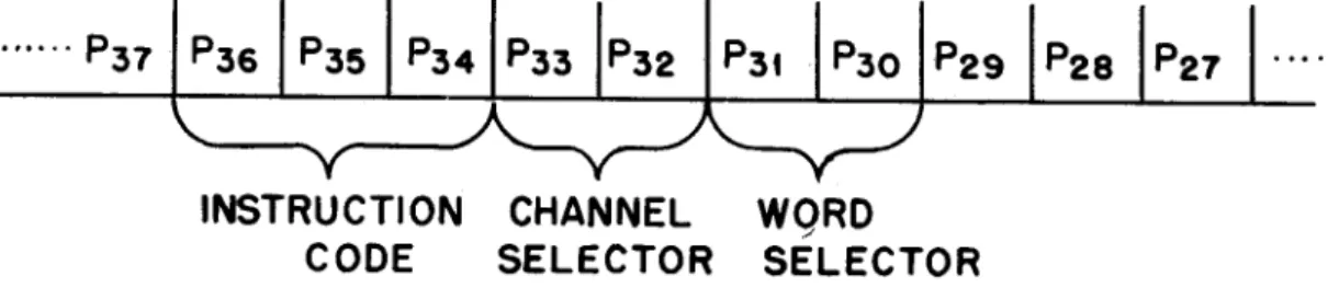
-The computer was designed to carry out only eight instructions, in order to keep the logical circuits. as simple as possible. Therefore, only the p30 to p36 positions of a word are decoded as an instruction. The p30 to p33 positions indicate the address of a memory location if the memory is to be involved in the instruction. Otherwise, these positions are not used by the computer. When a word from the memory is needed, the p32, p33 position indicate which of the four within the selected channel is to be read out. Thus, an address of 1000 would indicate the zero word of channel two. Or if we number the words from 0 (for the zero word of the zero channel) through 15 (for the 3 word channel of channel 3), 1000 would indicate word 8 of the memory.
The eight possible pulse combinations of the p30 to p36 position gives the code for the eight instructions the computer will execute.
Figure 33 indicates the portion of the word which the computer can use in in-struction.
INSTRUCTION
CODE
CHANNEL
SELECTOR
WQRD
SELECTOR
FIG. 33
The code is described as follows:
Instruction
OOOm
OOlm
010 0000
Description
Transfer the contents of the memory location in-dicated m to rA, clearing rA of its former con-tents and leaving (m) unaltered.
Transfer the contents of rA to the memory loca-tion indicated, clearing m of its former contents and leaving rA unaltered.
OHm
100m
101m
110 0000
111 0000
Transfer the address m of the instruction word from the static register to CC, clearing CC of its former contents.
/
Transfer the contents of memory location m to rB clearing rB of its former contents; transfer (rB) and (rA) to the adder and return the sum to rA,; clearing rA of its former contents and leaving rB unchanged.
Transfer (rA) and (rB) to the comparator leaving the contents of both registers unchanged: if
(rA)
>
(rB) transfer the address m of the in-struction word from the static register CC, clear-ing CC of its former contents, if rA L rB do not change CC.Shift (rA) one digit position to the right re-placing the sign position with binary zero. Shift (rA) one digit position to the left
re-placing the LSD with binary zero.
Organization of the Computer -The overall layout of the computer is shown in figure 34.
Memory - The main memory consists of four acoustic delay lines each capable of storing four words, or a total storage of sixteen words. These words can be instructions or data.
All instructions are stored in the memory as numbers, and are distinguished from data only by the manner in which the computer makes use of them. There is no section of the memory specifically allocated for instructions; data or instructions can be stored in any memory location.
It should be clearly understood that no arithmetic or logical operations are carried out in the memory. It is used only for storage. When a word stored in the memory is required as an operand or for decoding as an instruction, it must be transferred to the arithmetic circuits or control circuits.
The transmission line which carries information from the memory is called high speed ~ (HSB)lM. The line which transmits information to the memory is HSB2M.
ithmetic Circuits - These circuits consist of the algebraic adder (AA), the comparator CP), and two one-word acoustic type storages called register A, rA, and register B, rB. The latter serve as temporary storages for words to be used by the adder or comparator.
The comparator is used on the 101m order to compare the absolute values of rA and rB, and initiates one of two possible sequences of instructions based on
,
.j:>.'I'
Ir
~
1
r
STATIC REGISTERI I i , i i i
t t t t t ... t
CONTROL SIGNALS TO ARITHMETIC - LOGICAL COMPONENTS AND MAIN
MEMORY
A A
-t
ut t
"'-F" - - - ' ' - - - - ,
COMPAR
l-
r AI [
----~~-J
i i i i
HSB2A HSBtM
MASTER
OSCILLATOR
I I
t •
t
CYCLING UNIT
, , I ' ,
,
,
.'
,
TIMING SIGNALS TO ALL COMPONENTS
t6 WORD
MAIN MEMORY
• HSB1A
t
~HSBAt:
HSB2MThe adder is used on the 100m order to add or subtract the quantities stored in rA and rB, returning the sum to rAe It is also used by the control circuits to increase the word stored in the control counter (CC).
Control Circuits - The control circuits consist of the static register (SR), the cycling unit (CU), and the control counter (CC). The static register con-verts the p30 •••• p36 positions of a word to be used as an instruction into
flip-flop storage. These flip-flip-flops drive function tables to produce the necessary signals to carry out the instruction.
The cycling unit generates timing signals which are sent to all components of the computer to synchronize its operations.
The control counter is a one-word, mercury delay line register. Its purpose is to store the address of the next instruction word. The numerical value stored in CC is referred to as the CC-reading. Normally, the instructions are performed according to the numerical value of the memory locations in which they are stored. Thus, if CC initially reads zero, the computer is referred to 0000 for the first instruction word. As the reference to 0000 is completed, the CC-reading is advanced to 0001 and so forth. Hence, CC functions as the sequenc-ing mechanism of the computer.
If the normal sequence of instructions is to be changed, then the CC-reading must be altered. Both and Ollm and 101m orders accomplish this. (See
In-struction Code).
The transmission line which carries information to rA, rB, CC and SR is HSB2A. HSBlA receives information from rA, rB or CC and transmits it to the high speed bus amplifier (HSBA). This is primarily a switching central and can send infor-mation from HSBlA to HSB2A (for a register to register trans fer) or to HSB2M
(for a register to memory transfer).
Timing - Cycling
Quii
SignalsVJe have assumed a pulse rate of 1 Mg. for the computer. Pulses are produced at this frequency by a crystal controlled master oscillator, which maintains the pulse frequency with negligible variance. The pulse output of the master oscillator (one per ~ sec.) is not used to represent information directly, but controls all pulse formers in the computer to limit their output time for one information pulse to exactly one microsecond.
The propagation of information pulses through the various components of the ,computer will tend to distort them, but pulse formers are inserted sufficiently
I
~ ~
I
SIGNALS FROM
MASTER OSCILLATOR
SWITCH
rl
SINGLE PULSE ... DEVICETO O.F. FF
---..11·~ _ _ _ _ _ ___1 . . ._I1 PFR I ..
CYCLING UNIT
D221-rl Dt
t7
t6
t2
tt
FF
R S
i
t ...
t6 35
After the master oscillator is started, the single pulse device is switch operated. This produces one pulse whose duration is fixed at one microsecond by successive pulses from the master oscillator. The single pulse is fed into the recirculation loop of the cycling unit. This passes a PFR and a Dl delay and then produces a signal at tap A for one pulse time. The signal on this line is called a to and indicates the beginning of a minor cycle. After 42
~sec. or one minor cycle, the pulse once more reaches tap A and the to signal It; repeated.
Additional signals are needed at various time within the minor cycle and tnese are produced by tapping off the recirculation loop an appropriate amount of delay after the to.
For timing signals which last more than a pulse time, but which repeat each minor cycle, flip-flops controlled by CU signals can be used. Thus, a signal
is needed