3D-DATE: A Circuit-Level Three-Dimensional DRAM Area, Timing, and Energy Model.
Full text
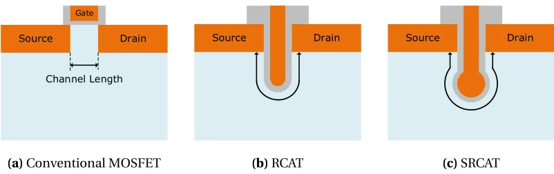
Figure
![Figure 2.2 3D Schematic diagram of VCAT-based DRAM cell [11].](https://thumb-us.123doks.com/thumbv2/123dok_us/1173692.1147531/23.612.186.447.79.316/figure-d-schematic-diagram-vcat-based-dram-cell.webp)
![Figure 2.6 MASTAR graphical user interface [47].](https://thumb-us.123doks.com/thumbv2/123dok_us/1173692.1147531/29.612.101.531.82.396/figure-mastar-graphical-user-interface.webp)
![Figure 2.7 Wire and wire cross section for resistance calculation [48].](https://thumb-us.123doks.com/thumbv2/123dok_us/1173692.1147531/31.612.129.502.383.584/figure-wire-wire-cross-section-resistance-calculation.webp)
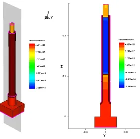
![Figure 2.10 Cross section and top view of single TSV with capacitance [53].](https://thumb-us.123doks.com/thumbv2/123dok_us/1173692.1147531/37.612.166.464.352.611/figure-cross-section-view-single-tsv-capacitance.webp)
Related documents
Workshop themes that have already been suggested by the program participants include: chaos in n-body systems, 3d radiative transfer, stability and origin of planetary systems,
A mail questionnaire was developed based on previous QOL and transportation research. The questionnaire was reviewed by MnDOT personnel and pre-tested with an online community
Reader’s guide; Introduction; Process of choices for scenarios; Scenario development; The national risk assessment; Confidentiality; Network of Analysts for National Safety
After enriching the knowledge assembly with information surrounding epilepsy, its risk factors, its comorbidities, and anti-epileptic drugs, a novel comparative mechanism
We performed a descriptive PK study using 11 sampling points, to assess the plasma pharmacokinetics of rifampicin, ethambutol, clarithromycin, azithromycin, isoniazid and
This study has the following aims: (1) to estimate the level of burnout among nurses working in PHC in the Andalusian Public Health Service; (2) to determine the phases of burnout
Additionally, actionable treatment or referral levels for phototherapy and exchange transfusion are proposed within the context of several confounding factors such as
This record contains information about how often the constraint was relevant for the ideal solution to the practice problems the student attempted, how often it was relevant for
