FPGA Implementation on High Speed Video DMA Engine
with Integrated IP Subsystem for Interfacing to Displays
K.Bindu Madhavi, V Moshe Rani
2,
Assistant Professor, HITAM,Hyderabad
Abstract:The main aim of this project is to use AXI4 Streaming protocol for Video and AXI memory map protocol for reading the frame buffer. The differentiation of Normal (System DMA) vs. Video DMA comes from the fact that Video DMA talks to Display module using AXI Streaming interface whereas normal DMA uses Memory map protocol to transfer data between memories via Interconnect or BUS protocol.
Key words: AXI Streaming, BUS protocol, AX14, Memory Map
1. INTRODUCTION:
The Video timing will be generating by programmable module for generating native video signals as per Display Monitor Timing standard. The Stream to Video Bridge converts the Streaming. Using the Video timing signals, the Native video output can be interfaced seamlessly to any display. The module hence designed can interface to any AXI compatible IP for optimal video use cases. Focuses on Design and Implementation of Display Sub-system (DSS) front end modules to interface seamlessly to any Display monitor and Frame buffer applications, using Industry Standard Advanced Extensible Interface (AXI4 Streaming) protocol. By using general purpose DMA (Direct Memory Access) engine for video lacks in optimization of Video Bandwidth to keep up with Memory bandwidth and high definition display rate. It needs External Video Timing Generator and protocol convertors for reading data from memory and converting to display format lacks standardization in interfacing to Video hardware accelerators like Scalar, Blender or Dis-play module. In this system, the following problems are addressed during this project work:
Integrating High Speed Video DMA engine with Display subsystem.
Design of modules like Video Timing Generator that generates necessary timing needed for interfacing to real world displays.
Adoption of high speed bus protocols like Advanced Extensible Interface (AXI) from ARM to Display subsystem.
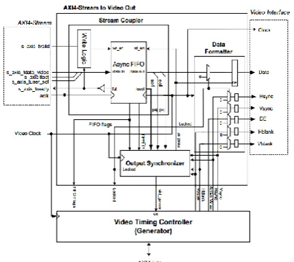
1.1 High Level System Overview:
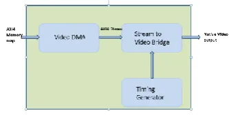
The overall block diagram of system is shown below. The basic components of system are Video DMA mod-ule, AXI4 Stream to Video Bridge and Video Timing generator. Video DMA (Direct Memory Access) module is a data mover that converts AXI4 Memory Map proto-col to AXI4 Streaming interface protoproto-col. AXI Stream to Video Bridge will take in AXIS Input and convert to Native Video output. It synchronizes Video timing with AXI4S data and produces timing output with data valid and pixel data. The system thus designed is targeted to be
implement on Zynq 7000 Series FPGA that has both Programmable Logic and Processing System with Cortex A9 ARM core. For interfacing to Zynq, Inrevium Dis-play port daughter card connected to Zynq through FMC connectors is used.
[image:1.595.341.508.310.394.2]
Figure 1: High Level Block diagram
AXI4 Memory map – Interface used to connect to DRAM (DDR2/DDR3) memory using an AXI based Interconnect. This interface will have a separate read and write channels. Each channel has its own address and data.
AXI4 Stream: This is a simple interface to avoid a lot of overhead involved in AXI4 Memory Map interface, and it has only data, valid and ready signals. The video sig-nalling needs only pixel data and pixel valid interface hence AXI4 Stream is a good fit for Video.
Other useful signals for Video like Start of Frame is sig-nalled by Video DMA using “USER” signal of AXIS protocol, and Video Timing generation(involving hsync, vsync, avid) is done by a “Timing Generator “ module, shown in above block diagram.
Native video output – An interface that is compatible to display monitors or digital video signalling involving (horizontal sync, vertical sync, active video enable, pixel clock and pixel data).
Tools Used: Xilinx Vivado14.1 (Synthesis, Implementa-tion and Bit stream GeneraImplementa-tion).
• ARM GCC Compiler (Low level driver compi-lation for CortexA9).
• Teraterm/HyperTerminal (For Debug Message logging).
• Questa (Simulation).
• Xilinx Chip scope (Emulation/ HW trace cap-ture).
• Division (Offline waveform /vcd analysis).
• Unit graph Display Port Analyser for DP proto-col debug while interfacing to Monitor.
1.2 Digital Video:
Initially, a digital Video usually contains both colour information and luminance or gray scale. If the colour information is removed, then it is left with gray scale, resulting in a black and white image. Gray scale is an important aspect of images, and it is the only the portion that is not removed; otherwise, a pure black image would result no matter what colour information there is. A digital image is composed of groups of three pixels with colours of red, green and blue (RGB), also called channels in digital imaging. Each channel also contains a luminance value to determine how light or dark the col-our is. To get a gray scale image, the colcol-our information from each channel is removed, leaving only the lumi-nance values, and that is why the image becomes a pat-tern of light and dark areas devoid of colour, essentially a black and white image. Most digital imaging software applications, even the most basic ones, are able to con-vert an image to gray scale. This is also very important when printing, since it only consumes black ink, as op-posed to printing in colour, which consumes all three print colours (cyan, magenta and yellow) as well as black.
[image:2.595.313.556.371.608.2]
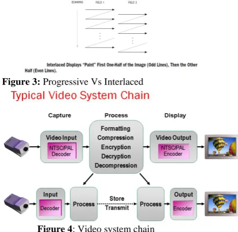
Figure 2: Video frame definition Interlaced vs. Progressive: Interlaced scanning
Interlaced scanning is simply displaying alternating sets of lines. First even numbered lines are displayed and then odd numbered lines are displayed. Each even set of lines are displayed for 1/60th of a second and then the odd lines are displayed for 1/60th of a second. This process is repeatedly. Each time an odd number series of lines will display and it is known as “field”. The same name is given to the even set of lines. Because each field happens so quickly, the illusion of a whole image is given. How-ever, very quickly; the other half of the image is present-ed.
Progressive video on the other hand displays the entire image in 1/60th of a second.
The consequences of using interlaced are predictable. Because of only capturing half of the image at a time, movement within the frame (due to either camera move-ment or subject movemove-ment) may cause motion artefacts. This happens especially when the movement is quick enough to cause noticeably different positions of the fields. For example, if you‟re filming interlaced from a moving car you‟ll notice motion artifacts.
Progressive scanning
Progressive video, as stated above captures 1 entire im-age per frame. This means you‟ll avoid the problem of motion artefacts. That being said, progressive video is not mainstream yet because it‟s more expensive. Howev-er, few camera models are reasonably affordable for in-dependent filmmakers. For about $3000, you can get the Panasonic AG-DVX100, which shoots progressive vid-eo. The Canon XL-2 is another option for shooting pro-gressive video.
Independent filmmakers desire progressive video be-cause the look of progressive resembles the look of film. Progressive scanning results in a clearer image and as mentioned above, progressive scanning handles move-ment differently. The cameras move-mentioned above also have the ability to shoot 24p, which also helps give your video the “film look” making it desirable to many filmmakers.
Figure 3: Progressive Vs Interlaced
Figure 4: Video system chain
[image:2.595.80.271.373.483.2]
Figure 5: Sample Video use case
1.3 Digital Video Interfaces:
[image:3.595.57.206.262.353.2]Digitized video is based on scan lines in found in analog video. BT.601 uses various sync signals to specify when a new field and a new line starts. BT.656 and BT.1120 uses sync words embedded in the data stream to specify start of field and start of line. An image can be digitized into regions shown in Figure 9 below:
Figure 6: Digital Video
[image:3.595.330.553.379.546.2]With the capability to encode sync words inside the data stream, there is more flexibility for adding non-video related data, called Ancillary Data. In addition, code words embedded in the digital stream could be used as a type of identifier for multiplexing several sources of vid-eo into one data stream. Such a multi-camera multiplex is useful in the digital security markets. The Field flag rep-resents the state of the Field ID for the picture. For pro-gressive frames, F is always „0.‟ The V flag specifies vertical blanking areas. The H flag specifies horizontal blanking portions of the picture.
Figure 7: FVH codes in Embedded Sync
Typical Display Interfaces (shown below) includes Co-axial input, S-video (this has separate Y and C signals), CVBS (Composite Video Blanking Sync) and Compo-nent Video.
Figure 8: Display Interfaces
2. INTRODUCTION TO AXI PROTOCOL: 2.1 AXI Architecture:
Advanced extensible Interface, or AXI, is part of ARM‟s AMBA specifications. The AXI is a point to point inter-connects that designed for high performance, high speed microcontroller systems. The AXI protocol depends on point to point interconnect to avoid bus sharing and therefore allow higher bandwidth and lower latency. AXI is arguably the most popular of all AMBA interface in-terconnect.
The essence of the AXI protocol is that it provides a framework for how different blocks inside each chip communicate with each other. It offers a procedure be-fore anything is transmitted, so that the communication is clear and uninterrupted. That way, different components can talk to each other without stepping on each other. The procedure for the AXI protocol is as follows: Master & slave must “handshake” to confirm valid sig-nals
Transmission of control signal must be in separate phases Separate channels for transmission of signals Continuous transfer is done through burst-type communication The following diagram shows a typical AXI bus connects. The processor is connected to the AXI inter-connect matrix via the AXI bus. The matrix can support multiple masters and multiple slaves.
By working with the master and slave devices, the AXI protocol works across five addresses that include read and write address, read and write data, and write re-sponse. Since each channel has its own unique signal, it can send the handshake response uninterrupted so that it can be received and put it into order. That way, the chan-nel that has priority will be responded first and so forth. The source must provide a valid signal and one that gets a proper response from the receiver.
By having the transmission performed in separate phases, it allows the transfer of information that to perform in an orderly manner. This means that a handshake or agree-ment reaches first, and then the information will be moved from the source to the recipient. In addition, that is how the AXI protocol works to move information be-tween different sources without interference.
[image:3.595.51.275.648.731.2]interface works, you can set the priorities for clear com-munication to occur.
AXI Interconnect:
The AXI protocol is burst-based. Every transaction has addressed and control information on the address channel that describes the nature of the data to transfer.
The data is transferred between master and slave using a write data channel to the slave or a read data channel to the master. In write transactions, in which all the data flows from the master to the slave, the AXI protocol has an additional write response channel to allow the slave to signal to the master the completion of the write transac-tion. The AXI protocol enables:
• Address information is ahead of the actual data transfer • Support for multiple outstanding transactions • Support for out-of-order completion of transactions.
Figure 12: Transaction channel and Handshake pair Channel definition: Each of the five independent chan-nels consists of a set of information signals and uses a two-way VALID and READY handshake mechanism. The information source uses the VALID signal to show when valid data or control information is available on the channel. The destination uses the READY signal to show when it can accept the data. Both the read data channel and the write data channel also include a LAST signal to indicate when the transfer of the final data item within a transaction takes place. Read and write address channels Read and write transactions each have their own address channel. The appropriate address channel carries all of the required address and control information for a trans-action.
The AXI protocol supports the following mechanisms: • Variable-length bursts, from 1 to 16 data transfers per burst
• bursts with a transfer size of 8-1024 bits
• Wrapping, incrementing, and non-incrementing bursts • Atomic operations, using exclusive or locked accesses • System-level caching and buffering control
• Secure and privileged access.
Read data channel: The read data channel conveys both the read data and any read response information from the slave back to the master.
The read data channel includes:
• the data bus, that can be 8, 16, 32, 64, 128, 256, 512, or 1024 bits wide
• a read response indicating the completion status of the read transaction.
The architecture for reads is shown below:
Figure 09: AXI Read
Write data channel: The write data channel conveys the write data from the master to the slave and includes: • The data bus, that can be 8, 16, 32, 64, 128, 256, 512, or 1024 bits wide
• one byte lane strobe for every eight data bits indicates that which bytes of the data bus are valid. Write data channel information will be treated as buffer, so that the master can perform write transactions without slave acknowledgement of previous write transactions.
The architecture for writes is shown below:
Figure 10: AXI Write
Write response channel: The write response channel pro-vides a way for the slave to respond to write transactions. All write transactions use completion signalling. The completion signal occurs once for each burst, not for each individual data transfer within the burst.
2.3 AXI Streaming Adoption for Video:
AXI4-Stream Video is a subset of AXI4-Stream de-signed for transporting video frames. AXI4-Stream Vid-eo is compatible with AXI4-Stream components; it simp-ly has conventions for the use of ports already defined by AXI4-Stream:
The TLAST signal designates the last pixel of each line, and is known as end of line (EOL).
The TUSER signal designates the first pixel of a frame and is known as start of frame (SOF). These two flags are necessary to identify pixel locations on the AXI4 stream interface because there are no sync or blank signals. 3. Video DMA component makes use of the TUSER signal to synchronize frame buffering. Note that TUSER flag which is part of AXI4-Stream specifica-tion replaces FSYNC signal that has been used in the past by legacy applications.
Figure 13: Video system chain 2.4 AXI Streaming Signalling Protocol:
This describes that how the interface signals can be used and basic protocols of the AXI4-Stream specification to construct streaming interfaces that meets the needs of various video system applications. Generally AXI proto-col signals are defined using signal names reflecting their video specific function.
Channel Structure:
This interface consists a set of handshake signals namely VALID and READY, and a set of information-carrying signals, DATA, EOL, and SOF, which are conditioned by the handshake signals.
These signals must operate in the same clock domain. The master and slave side can operate in different clock domains.
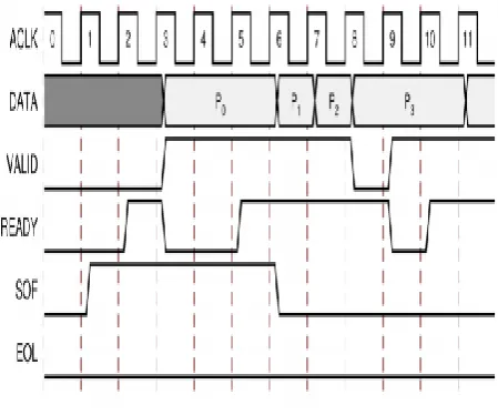
READY and VALID Handshake:
A valid transfer takes place when READY, VALID, ACLKEN, and ARESET signals are high at the rising edge of ACLK, as shown in Figure 14. During valid transfers, DATA only carries active video data.
Figure 14: AXI4 Stream timing diagram
Start of Frame Signal - SOF
The first pixel of a video frame marked by physically transmitted over the AXI4-Stream TUSER0 Signal using the Start-Of-Frame (SOF) signal. The SOF operations are the following:
• It serves as a frame synchronization signal, that allows downstream cores to re-initialize, and to detect the first pixel of a frame.
• As long as a VALID is not asserted, it can be asserted an arbitrary number of ACLK cycles before the first pix-el value is presented on DATA.
End of Line Signal - EOL
The End-Of-Line (EOL) signal, physically transmitted over the AXI4-Stream TLAST signal, marks the last pix-el of a line. The EOL pulse is 1 valid transfer wide, and must coincide with the last pixel of a scan line.
[image:5.595.51.276.441.628.2]The data format representations marked on to main link are shown below:
Table 1: Video format mapping on AXI Streaming data bus
2.5 AXI Stream to Video bridge:
In the slave mode, the AXI4-Stream to Video Out core input is an AXI4-Stream interface. This consists of paral-lel video data, tdata, handshaking signals like tvalid and tready, and two flags namely tlast and tuser. This will serve to identify certain pixels in the video stream. The last signal gives the last valid pixel of each line, and is known as the end of line (EOL). The tuser signal gives the first valid pixel of a frame, and is known as start of frame (SOF).
Figure 15: AXI4 Stream to Video out core
2.6 Display Port Standard:
A Display Port link mainly consists of three parts. They are main link, an auxiliary channel (AUX CH), and a Hot Plug Detect (HPD) signal line. The Main Link is a unidi-rectional link with high-bandwidth and low-latency channel. It is used to transport isochronous data such as uncompressed video and audio. The auxiliary channel is a half-duplex bidirectional channel and is used in link management and device control. HPD signal also serves as an interrupt request by the Sink device. In addition, the DP connector for a box-to-box connection has a power pin for powering either a DP repeater or a Display Port-to-Legacy converter.
[image:6.595.52.297.457.641.2]Figure 16: Display Port overview DP Architecture:
Figure 17: DP Layered modular architecture Isochronous Transport Services
The isochronous transport services of the link layer pro-vide the following:
1. Mapping of stream data to and from Main Link lanes 2. Packing and unpacking
Stuffing and unstuffing Framing and unframing
Inter-lane skewing and de-skewing
3. Stream the clock recovery data and attributes data
3. XILINX VIVADO DESIGN FLOW
The Flow Navigator provides access to commands and tools to take design from design entry to bit stream crea-tion. The different sections in the Flow Navigator enable you to do the following:
Figure 18: Vivado Flow Navigator 3.1 Creating Vivado Projects:
The below are detailed steps needed to fully create and build a project:
Step 1: Invoke the Vivado IDE and Create a Project: Invoke the Vivado IDE by clicking the desktop icon or by typing vivado at a terminal com and line.
Figure 19: Vivado IDE
The New project wizard opens as shown below:
Figure 20: Vivado project wizard
In the Project Type dialog box, select RTL Pro-ject. Click Next.
In the Add Sources dialog box, ensure that the Target language is set to Verilog. Click Next. In Add Existing IP dialog box, click next. In Add Constraints, dialog box click next. In the Default Part dialog box select Boards and
Project Summary dialog box before clicking Finish.
Step 2: To Create an IP Integrator Design
Go to Flow Navigator - IP integrator, and select Create Block Design. Specify the IP subsystem design name, and click OK.
Figure 21: Vivado IPI design
Once IPs is added and connections made, the example block diagram looks as below:
Figure 22: Vivado Block design Step 3: Create Constraints
In the Flow Navigator, go to the Project Manager. Open the Constraints folder. Right-click the constrs_1 folder, then select Edit Constraints Set.
Step 4: Memory Mapping the Peripherals in IP Inte-grator
In the Project Manager, double-click the design name under
Design Sources to open the design. Click the Address Editor tab. In the Address Editor, map any unmapped devices by doing the following:
a. Expand the Micro Blaze IP.
b. Right-click the Unmapped Slaves folder, and select Auto Assign Address.
Step 5: Creating a Top-Level Verilog Wrapper Go to the Project Manager. Under Design Sources, right-click your design and right-click Create HDL Wrapper. Step 6: Take the design through implementation In the Flow Navigator:
Click Run Synthesis.
Click Run Implementation. Click Generate Bit stream
PHASE1a AXI2 VIDEO + TIMING_GEN IMPLE-MENTATION):
Design and simulation of AXI to VIDEO bridge with Video Timing controller driven by Test Pattern Genera-tor on Xilinx Vivado 2013.4
[image:7.595.58.267.143.316.2]
Figure 23: Design of AXI2VIDEO bridge
Figure 24: Video Timing Generator simulation results
[image:7.595.56.225.370.517.2]State Machine for AXI42VIDEO bridge:
Figure 25: AXI42VIDEO State machine
Figure 26: AXI42VIDEO simulation results RTL Synthesis output:
Figure 27: AXI42VIDEO + TIMING GEN synthesis output
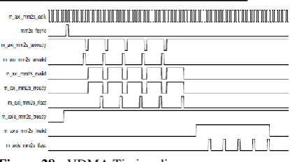
[image:8.595.114.526.56.698.2]PHASE1b VDMA IMPLEMENTATION:
Figure 28: VDMA Timing diagrams Final System design):
[image:8.595.342.539.69.476.2]The Vivado IPI design is shown below after integrating with ZYNQ 7000 + VDMA + AXI42VIDEO BEIDGE + VIDEO TIMING GENERATOR.
Figure 29: Display Sub system design Utilization:
[image:8.595.315.533.432.676.2] [image:8.595.51.259.467.583.2]Figure 31: Display Sub system emulation traces The snapshot of Zynq board is shown below:
[image:9.595.61.264.470.587.2]Figure 32: Zynq board
And the Display Port card is an add on card that interfac-es to Display monitor via FMC-HPC connector.
Figure 33: Inrevium board with Display port interface
The low-level driver will be implemented along the flowchart shown below:
4. ENABLING MAIN LINK VIDEO:
a. Main link video is not enabled until a proper vid-eo source is provided with the source core. b. Typically the source device will want to read the
EDID from the attached sink device to determine its capabilities, most importantly its preferred res-olution and other resres-olutions that it supports should the preferred mode not be available. c. Once a resolution has been determined, set the
Main Stream Attributes in the source core (0x180 - 0x1B0).
5. CONCLUSION AND FUTURE SCOPE Conclusion:
• Design / Integration and Simulation of Timing generator module, Video Bridge and Video DMA is done and implemented on Xilinx Zynq 7000 FPGA.
• System brought up on Xilinx FPGA and inter-faced to a real time Display Port Monitor.
• Software Implementation in C language for Video DMA, Timing generator and Display module for sending HD Video frames to a Dis-play unit (DisDis-play Manager) is done.
• Targeted application of High performance 1080P frame rate of around 700MBPS has been achieved.
Future Scope:
• Multi-channel video application, Alpha blend-ing are further scope of expansion of this Mod-ule.
• Integrating to AXI Compatible Video hardware accelerators like Chroma sampling, Noise Filter, on the fly scaling etc. are good fit to be inter-faced with this module, to render various Video use cases.
REFERENCES:
[1] "Foundation Series ISE 3.1i User Guide" (PDF). [2] Handbook of Networked and Embedded Control
Systems, Springer Science & Business Media, 14-Nov-2007
[3] Circuit Design with VHDL, MIT Press, 2004 [4] Advances in Computer Science and Information
Engineering, Springer Science & Business Media, 11-May-2012
[5] Embedded Systems Design with Platform FPGAs, Morgan Kaufmann, 10-Sep-2010
[6] "Xilinx Inc, Form 10-K, Annual Report, Filing Date May 25, 2012". Secdatabase.com. Re-trieved May 6, 2018.
[7] Vivado Design Suite, First version released in 2012, Xilinx Downloads
[8] FPGA Prototyping By Verilog Examples, John Wiley & Sons, 20-Sep-2011
[9] The Digital Consumer Technology Handbook, Elsevier, 30-Apr-2004
[10] "Xilinx Product Table correction". [11] "ISE Design Suite Product Table" (PDF). [12] "Xilinx ISE Webpack 11". Gentoo Wiki. Gentoo
Community. Archived from the original on Octo-ber 7, 2012. Retrieved 8 May 2012.
[13] "Xilinx ISE WebPACK". Arch Wiki. Arch Com-munity. Retrieved 8 May 2012.
[14] "Installed Xilinx ISE WebPack 12.1 on Fedora 12 x86_64". What's All This Brouhaha? Word-press. Archived from the original on March 3, 2011. Retrieved 8 May 2012.