A Review- Power Reduction Using Data
Encoding Schemes in Network on Chip
Nikita Dahake, Radhika Harne
PG Student, Dept. of Electronics and Telecommunication, Government College of Engineering, Amravati, India
Assistant Professor, Dept. of Electronics and Telecommunication, Government College of Engineering, Amravati,
India
ABSTRACT: The power dissipation of links of network on chip increases as the technology going to reduce. This
power dissipation is even larger than other elements of communication subsystem like router and network interface. Here, in this paper we represent three different data encoding schemes which are helpful for reducing power dissipation by links of network on chip. The proposed system gives reduction in dynamic power dissipation by reducing coupling switching activity and switching activity when compared to previous system. Also, the proposed scheme does not need any type of modification of the routers and link architecture. Using this, power dissipation and energy consumption will be reduced without any significant performance degradation.
KEYWORDS: Data encoding; coupling switching activity; network-on-chip (NoC); low power, power analysis.
I. INTRODUCTION
As semiconductor technology scales to nanometer technology, power requirement becomes a critical factor in digital system. Network on chip is a communication system on integrated circuit between IP cores in a system on a chip (SOC). NoC technology is applied method for on-chip communication and brings improvement over conventional bus and crossbar interconnections. The network on chip (NoC) design paradigm is recognized as the most promising way to solve the scalability and variability problems that defines the ultra deep submicron meter era. As the design complexity increases, the total length of the interconnection wires increases which results in long transmission delay and higher power consumption.
In this paper, the main focus is on reduction of power dissipation caused by network links. In fact, the power dissipated by the network links is as large as that dissipated by network interfaces and routers and it will increase in near future nodes as technology scales. In particular, we present different designs of encoders which operates at flit level and works on end-to-end basis, which makes it easier to decrease both the switching activity and the coupling switching activity on links of the routing paths followed by the packets. We focus on data encoding schemes as a possible way to reduce dissipation of power by the links of network. The basic idea is to just encode the data before their injection in the network in such a way that it will reduce the switching activity of the links. Silicon area, reduction in power and energy are the parameters which are taken into consideration for analysis. The results show that by using this proposed encoding schemes power and energy can be saved.
II.RELATED WORK
activity and avoids the dissipation of power. Bus invert [BI], INC-XOR these are proposed methods used for random patterns of data transmission via lines. While, gray code, T0, working-zone encoding, and T0-XOR are methods for correlated data patterns. Out of total interconnects capacitance if the coupling capacitance is a major part then this category of encoding is not applicable for deep sub-micron meter technology nodes.
Second category focus on reducing power dissipation caused by the coupling switching. Power effective Bus Invert come under this category. It presented a method based on Odd/Even Bus-Invert techniques. The coupling capacitances between on-chip bus lines become dominant in deep-submicron meter technologies. Coding to reduce the switching activity of the individual lines was enough to reduce power on buses in older technologies, but new coding techniques that reduce the coupling activity between lines are needed for deep-submicron buses. A coding technique that reduces the coupling switching activity by taking the advantage of end-to-end encoding for wormhole switching has been presented in “Data encoding schemes in networks on chip” [9]. It is based on lowering the coupling switching activity by eliminating only Type II transitions.
III. PROPOSED METHOD
The proposed method suggest to encode flits before sending them into the network. Because of self-switching and coupling switching activity link power is more dissipated. In this project, there is end-to-end scheme, means flits which passes through the links of the routing path are encoded first at network interface [6]. Encoder and decoder block are added at network interface level. The encoder encodes all the outgoing flits of the packet except header flit so that power dissipation in path of inter router is getting reduced [9].
This encoding technique is proposed to reduce power dissipation by minimizing both, self and coupling switching activities on the links of interconnected network. In this paper, three encoders are designed using three different schemes.
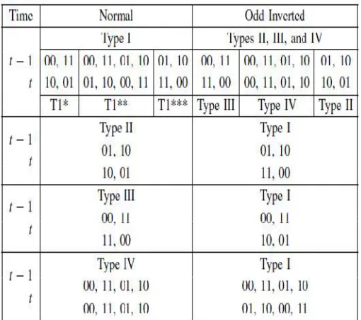
Table 1.Effect of odd inversion on change of transition types
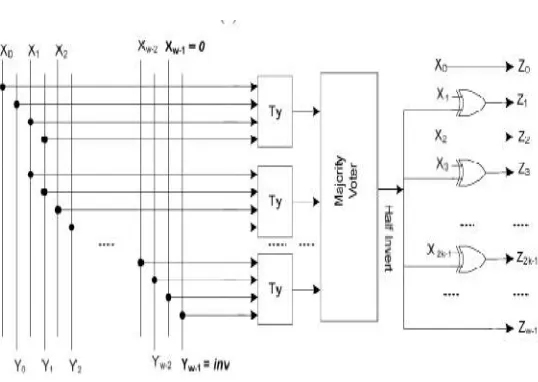
Fig 1. Encoder architecture
The encoder architecture in Fig. 1 for scheme 1, scheme 2 and scheme 3 is same. The encoder block gets w-1 bit as one of the input and previous encoded output is another input. Then comparison is done between these two inputs by encoder block and then any one of the inversion operation is performed based on the transition types.
IV. Scheme I
Fig 2. Encoder block internal view scheme I.
In scheme I, we concentrate on minimizing the number of Type I transitions (by transforming them into Types III and IV transitions) and Type II transitions (by transforming them into Type I transition). The scheme compares the current data with the previous one to decide whether odd inversion or no inversion of the current data can lead to the link power reduction.
If the flit is odd inverted before being transmitted, the dynamic power on the link is
where T0→1, T1, T2, T3, and T4 are the self-transition activity, and the coupling transition activity of Types I, II, III, and IV respectively.
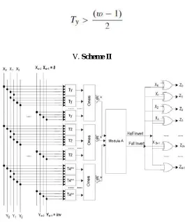
V. Scheme II
Fig 3. Encoder block internal view scheme II
Here, in this proposed encoding scheme, we utilise both odd as well as full type of inversion. In full inversion operation, there is conversion of Type II transition into Type IV transition. There is comparison made of current data with the previous data and after that decision will be made to convert current data into odd, full or no inversion. So that finally, we will get least power dissipation. The previously encoded body flit is show by the wth bit in that, inv which tells if odd or full inversion operation is done (inv = 1) or left as it was (inv = 0).
Now, indicate P, P' and P'' for the power dissipation by the link at a time when the flit is transmitted with no inversion, odd and full inversion, respectively. Power reduction occur in odd inversion condition when
P' < P and P' < P'', odd inversion condition is obtained as,
full inversion condition is as,
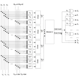
VI. SCHEME III
Figure 4. Encoder block internal view scheme III Full inversion Condition is,
odd inversion condition is,
When none of condition is satisfied, no inversion will be performed.
VII. CONCLUSION AND FUTURE WORK
REFERENCES
1. Nima Jafarzadeh, Maurizio Palesi, Ahmad Khademzadeh and Ali Afzali-Kusha, “Data Encoding Techniques for Reducing Energy Consumption in Network-on-Chip” IEEE transactions on very large scale integration (VLSI) SYSTEMS, vol. 22, no. 3, MARCH 2014. 2. Z. Khan, T. Arslan, and A. T. Erdogan, “Low power system on chip bus encoding scheme with crosstalk noise reduction capability,” IEEE
Proc. Comput. Digit. Tech., vol. 153, no. 2, pp. 101–108, Mar. 2006.
3. K. Banerjee and A. Mehrotra, “A power-optimal repeater insertion methodology for global interconnects in nanometer designs,” IEEE Trans. Electron Devices, vol. 49, no. 11, pp. 2001–2007, Nov. 2002.
4. M. S. Rahaman and M. H. Chowdhury “Crosstalk avoidance and error correction coding for coupled RLC interconnects,” in Proc. IEEE Int. Symp. Circuits Syst., May 2009, pp. 141–144.
5. W. Wolf, A. A. Jerraya, and G. Martin, “Multiprocessor system-on-chip MPSoC technology,” IEEE Trans. Comput. Aided Design Integr. Circuits Syst., vol. 27, no. 10, pp. 1701–1713, Oct. 2008.
6. L. Benini and G. De Micheli, “Networks on chips: A new SoC paradigm,” Computer, vol. 35, no. 1, pp. 70–78, Jan. 2002.A. Vittal and M. Marek-Sadowska, “Crosstalk reduction for VLSI,” IEEE Trans. Comput.-Aided Design Integr. Circuits Syst., vol. 16, no. 3, pp. 290–298, Mar. 1997.
7. M. R. Stan and W. P. Burleson, “Bus-invert coding for low-power I/O,” IEEE Trans. Very Large Scale Integr. (VLSI) Syst., vol. 3, no. 1, pp. 49–58, Mar. 1995.
8. M. Palesi, G. Ascia, F. Fazzino, and V. Catania, “Data encoding schemes in networks on chip,” IEEE Trans. Comput.-Aided Design Integr. Circuits Syst., vol. 30, no. 5, pp. 774–786, May 2011.
9. A Vittal and M. Marek-Sadowska, “Crosstalk reduction for VLSI,” IEEE Trans. Comput.-Aided Design Integr. Circuits Syst., vol. 16, no. 3,pp. 290–298, Mar. 1997.
10. L. Macchiarulo, E. Macii, and M. Poncino, “Wire placement for crosstalk energy minimization in address buses,” in Proc. Design Autom.Test Eur. Conf. Exhibit., Mar. 2002, pp. 158–162.
BIOGRAPHY
Nikita Sanjay Dahake is a M.Tech student in the of Electronics and Telecommunication department, Government