Department of Electrical & Electronics Engineering, College of Engineering Perumon, Kollam, Kerala – 691601, India
Modelling and Simulation of Novel 25 Level
Inverter with Single DC Source
Viji Chandran, Kannan S A1, Edwina Rodrigus2, A R Arya3, Athira Manidas4, Judith Bencilien5, Divya S6,
Nithya Chandran7
Assistant Professor, Department of Electrical and Electronics Engineering, College of Engineering Perumon, Kollam,
Kerala, India1,2
B.Tech Scholars, Department of Electrical and ElectronicsEngineering,College of Engineering Perumon, Kollam,
Kerala, India3-7
ABSTRACT: The major problem faced in today’s world is energy scarcity. Since the conventional energy sources are diminishing, more focus is towards alternate energy source. DC power is converted into AC power using inverters. Main issues that related to the conventional inverters are non-sinusoidal output, high total harmonic distortion (THD), high switching stress, loss and more number of switches. So multilevel inverter (MLI) have much importance over conventional inverters. The topology used is the cascaded H bridge 25 level inverter with single DC source using SPWM technique. 25 output levels using 10 switches with near sinusoidal voltage can be obtained with a single DC source. The advantages of this topology are Low THD, voltage stresses, small common mode voltage and operated with lower switching frequency
KEYWORDS: PWM-pulse width modulation, MLI-multi level inverter,THD-total harmonic distortion
I..INTRODUCTION
All nations over the world are engaged in solving the problem of energy crisis due to the depletion of fossil fuels. Combustion of non renewable energy sources like fossil fuels leads to pollution.This has ignited the spark of green energy concept with the use of renewable energy sources. Plenty of researches are being carried out to harvest the renewable energy. Compared to other types of renewable energy sourcessolar energy has wide importance as it is pollution free and freely available. Solar energy is trapped by PV arrays and it is converted into electoral energy . The output obtained from the PV arrays in in DC form. The high gain DC-DC boost converter stepped up the DC output voltage and then connected to inverters for DC to AC conversion. A Power inverter is an electronic device or circuitry that changes DC (direct current) to AC (Alternating Current). Conventional two-level inverter creates two different output voltages Vdc2 and -Vdc2 when fed with a DC voltage Vdc. To build an AC output voltage, these two voltages are usually obtained using PWM (Pulse Width Modulation).
Department of Electrical & Electronics Engineering, College of Engineering Perumon, Kollam, Kerala – 691601, India At present the most famous hardware implementable topologies are cascaded H-bridge and the diode clamped. Though this method is effective, yet it creates harmonic distortions on the output voltage, EMI (Electro Magnetic Interference) and high dv/dt. When it comes to multilevel inverter modulation there are basically two groups of methods: modulation with fundamental switching frequency or high switching frequency PWM . For both cases a stepped output waveform is achieved, but with the high switching frequency methods the steppes are modulated with some sort of PWM . Independent of switching frequency choice there are also space vector methods to choose from. Multilevel PWM methods uses high switching frequency carrier waves in comparison to the reference waves to generate a sinusoidal output wave, much like in the two-level PWM case.
To reduce harmonic distortions in the output signal phase-shifting techniques are used . There are several methods that change disposition of or shift multiple triangular carrier waves. The number of carrier waves used is dependent to the number of switches to be controlled in the inverter. The Phase Shifted Carrier PWM (PSCPWM), is a multi carrier modulation strategy that has all carrier waves phase shifted from each other. But In Phase Distortion PWM (PDPWM), all carrier waves are in phase. A great acknowledgement for this technique is that it is generally accepted as the method that creates the lowest harmonic distortion in line-to-line voltage. The proposed topology contains minimum number of switches for generating same output levels as compared to conventional MLI.
II. RELATED WORKS
Multilevel inverter technology has emerged recently as a very important alternative in the area of high power mediumvoltage energy control and grid connected applications. Three basic topologies are;
1. Diode clamped
2. Flying capacitor
3. Cascaded H- bridge Multilevel inverters
. An attempt has made in [8] to propose a new structure for the multilevel inverter with the reduced number of
power electronic devices compared to the conventional type of cascade inverter. But this inverter requires large number of bidirectional switches and also its magnitude of blocked voltage is high .In [8] different structures of bidirectional switch combinations also explained
. In [10], another topology for cascade multilevel converter has been introduced. It reduces the number of bidirectional switches, power diodes, and dc voltage sources compared with [9]. But this topology requires large number of gate driver circuits and switches. It consists of several submultilevel converters and full-bridge converters.
R. ShalchiAlishah et al. proposed topologies for symmetric, asymmetric, and cascade switched-diode multilevel inverters in [11]. It has more advantages in comparison with the topologies in the [8], [10]. When compared with the proposed topology, it requires more number of fast recovery diodes and separate dc sources. The modulation technique used is a fundamental switching strategy, a low switching frequency compared to other control techniques.
A.PROBLEM IDENTIFICATION
Multilevel inverter technology has emerged recently as a very important alternative in the area of high-power medium-voltage energy control and grid connected applications.Three basic topologies are; Diode clamped, Flying capacitor and Cascaded H-bridge Multilevel inverters. But these 3 topologies have several drawbacks.
The drawbacks of diode clamped multi level inverter are Real power flow is difficult for a single inverter; the number of clamping diodes required is quadratically related to the number of levels and Expensive The disadvantages of flying capacitors are Control is complicated to track the voltage levels for all of the capacitors. Pre charging all of the capacitors to the same voltage level and start up are complex. Switching utilization and efficiency are poor for real power transmission. The large numbers of capacitors are both more expensive and bulky than clamping diodes in multilevel diode-clamped converters. Packaging is also more difficult in inverters with a high number of levels
Department of Electrical & Electronics Engineering, College of Engineering Perumon, Kollam, Kerala – 691601, India
III.PROPOSED MLI
The proposed topology consists of two converter stages namely: the flyback converter and the cascaded H-bridge inverter.
Fig 1.Circuit diagram of proposed MLI
The complete circuit diagram of the proposed MLI under the stand-alone mode is shown in Fig. 1. In conventional symmetric CHB MLI, the voltage levels of the isolated DC sources are equal. Meanwhile, in asymmetric inverters, the sources are not equally distributed. Although symmetric multilevel inverters have the advantage of a simple controller, asymmetric multilevel inverters can produce a higher number of voltage levels with the same number of H-bridge modules.
Fig.1 shows MLI where 25 output levels are obtained by using only 10 switches. This arrangement can be further augmented by cascading 'P' number of basic cells in series. As the number of output levels is increased the output approaches close to sinusoidal waveform. This topology contains two cascaded basic cells. Each cell consists of two equal voltage sources. The voltage sources of second basic cell are in ratio of l:5 with respect to voltage sources of first basic cell. This topology helps to generate 25 output levels. This arrangement is defined as asymmetric MLI because of unequal voltage sources in two respective basic cells.
The 25-level inverter consists of two cascaded basic units. Each unit consists of two equal voltage input from the flybackconverter. The voltage input to the first unit to the second is in the ratio of 1:5. This topology helps to generate 25 level output. The 1:5 ratio is maintained by the proper turns ratio (1:5)in the transformer winding of the flyback converter. Let n1 = n, then n2 = n, n3 = 5n, n4 = 5n. This arrangement leads to an unequal voltage input to the two respective basic units (asymmetrical MLI).
V11 = V12 = Vdc
V21 = V22 = 5Vdc
Vm1 = Vm2 = 5(m-1)×Vdc
The proposed structure requires a multi-output flyback converter and a 25-level inverter. The output of the flyback inverter is fed to the MLI. It requires 10 switches for the MLI and one switch for the flyback converter for its operation.
A. OPERATION OF PROPOSED STRUCTURE
Department of Electrical & Electronics Engineering, College of Engineering Perumon, Kollam, Kerala – 691601, India converter. The transformer windings also depend on the load voltages. The operation of the proposed MLI is illustrated in the Table 1.
Table1 Switching states
The switches S15 and S25 are the selection switches to add the number of output levels. The basic units are connected
in series to form cascade structure. The output of each basic unit is added together to achieve the final output voltage voltage.
B. MODULATION TECHNIQUES
Department of Electrical & Electronics Engineering, College of Engineering Perumon, Kollam, Kerala – 691601, India
Fig. 2 POD SPWM technique
IV. SIMULATION RESULTS
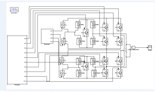
The simulink model of the proposed 25 level inverter using a single source is shown in Fig. 4. The simulations are performed using MATLAB. The simulink model mainly consists of the multilevel inverter circuit, subsystem for the pulses generation and subsystem for the multi-output flyback converter. In this system R-L load is used as load.
Fig. 3 Simulink model of proposed structure
Department of Electrical & Electronics Engineering, College of Engineering Perumon, Kollam, Kerala – 691601, India
Fig 4. Subsystem of POD SPWM
The output voltage obtained is shown in Fig.5.The maximum output voltage obtained in this structure is the sum of the load voltages of the multi-output flyback converter. The output voltages of flyback converter is given by figure 6.
. Fig 5. Output of proposed structure
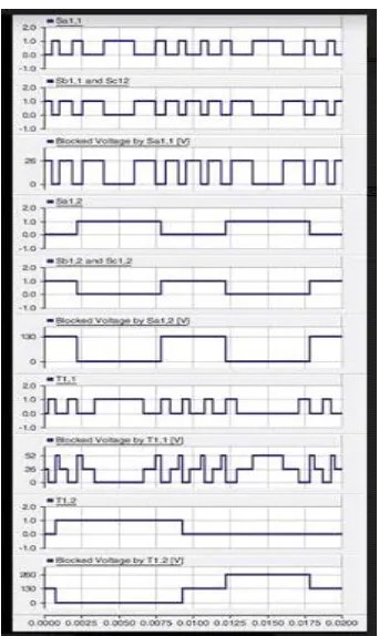
Department of Electrical & Electronics Engineering, College of Engineering Perumon, Kollam, Kerala – 691601, India The gate pulse to the switches in the MLI is shown in Fig.7. The multilevel inverter requires 10 switches for twenty five level output. The pulses generated are by using the POD-SPWM technique. The corresponding pulses are given to switches S11, S12, S13, S14, S15, S21, S22, S23, S24 and S25 respectively in the Fig.7.
Fig 7.switching pulses of proposed modulation scheme
The resulting total harmonic distortion of the proposed structure is shown in Fig. 8. The THD of this structure is 4.76%. The total harmonic distortion is very less compared to conventional type cascade inverters.
Department of Electrical & Electronics Engineering, College of Engineering Perumon, Kollam, Kerala – 691601, India
V. CONCLUSION
In this paper, a cascaded multilevel inverter is proposed which requires minimum number of switches with increased output levels where, output waveform is near-sinusoidal. Compared with conventional multilevel inverters, it requires less number of components to achieve same number of output levels. Overall THD is very low and thus the quality of output waveform is improved. Due to the use of fewer switches, optimized circuit layout and packaging is possible. Thus less Cost is required to implement the proposed inverter. When sinusoidal pulse width modulation (SPWM) technique is installed THD value will reduce even further. This topology can be successfully installed for solar based ac applications. The operations of the cascaded MLI using the flyback converter have been verified by MATLAB software.
REFERENCES
[1] J. Rodriguez, J. S. Lai, and F. Z. Peng, “Multilevel inverters: A survey of topologies, controls, applications,” IEEE Trans. Ind. Electron., vol. 49, no. 4, pp. 724–738, Aug. 2002.
[2] Z. Du, B. Ozpineci, L. M. Tolbert, and J. N. Chiasson, “DC–AC cascaded H-bridge multilevel boost inverter with no inductors for electric/hybrid electric vehicle applications,” IEEE Trans. Ind. Appl., vol. 45, no. 3, pp. 963–970, May/Jun. 2009.
[3] G. Buticchi, D. Barater, E. Lorenzani, C. Concari, andG.Franceschini, “A nine-level grid-connected converter topology for single-phase transformerless PV systems,” IEEE Trans. Ind. Electron., vol. 61, no. 8, pp. 3951–3960, Aug. 2014.
[4] W. Song and A. Q. Huang, “Fault-tolerant design and control strategy for cascaded H-bridge multilevel converter-based STATCOM,” IEEE Trans. Ind. Electron., vol. 57, no. 8, pp. 2700–2708, Aug. 2010.
[5] Y. Xiaoming and I. Barbi, “Fundamentals of a new diode clamping multilevel inverter,” IEEE Trans. Power Electron., vol. 15, no. 4, pp. 711– 718, Jul. 2000.
[6] J. Hunag and K. Corzine, “Extended operation of flying capacitor multilevel inverters,” IEEE Trans. Power Electron., vol. 21,no. 1, pp. 140–147, Jan. 2006.
[7] M. N. Abdul Kadir, S. Mekhilef, and H. W. Ping, “Dual vector control strategy for a three-stage hybrid cascaded multilevel inverter,” J. PowerElectron., vol. 10, no. 2, pp. 155
–164, 2010.
[8] E. Babaei, “A cascade multilevel converter topology with reduced number of switches,” IEEE Trans. Power Electron., vol. 23, no. 6, pp. 2657– 2664, Nov. 2008
. [9] E. Babaei, S. H. Hosseini, G. B. Gharehpetian, M. T. Haque, and M. Sabahi, “Reduction of DC voltage sources and switches in asymmetrical multilevel converters using a novel topology,” J. Elect. Power Syst. Res., vol. 77, no. 8, pp. 1073–
1085, Jun. 2007.
[10] J. Ebrahimi, E. Babaei, and G. B. Gharehpetian, “A new multilevel converter topology with reduced number of power electronic components,” IEEE Trans. Ind. Electron., vol. 59, no. 2, pp. 655–667, Feb. 2012.