ABSTRACT
PHELPS, BRIAN ROBERSON. Hardware realization and implementation issues for the
Sliding-Window Packet Switch (Under the direction of Dr. Paul D. Franzon)
Shared memory packet switches are known to provide the best delay-throughput and
respond well to bursty traffic. Shared memory switches are also known to scale poorly due
to centralized control and memory bottlenecks. The Sliding Window Packet Switch (SW)
algorithm is a shared memory switch that employs decentralized control and multiple
memory modules to facilitate the scalability of hardware. The SW algorithm is independent
of the type of packet or cell.
This research has two closely related goals. The first goal is to implement the SW
algorithm in hardware such as an FPGA. This implementation is actually a specific case of
the SW algorithm with four input ports and four output ports (i.e. a 4x4 switch). The second
goal is to determine what scalability constraints exist in hardware for larger numbers of input
and output ports (large NxN). These constraints are used to predict the overall throughput
HARDWARE REALIZATION AND IMPLEMENTATION ISSUES FOR THE
SLIDING-WINDOW PACKET SWITCH
by
BRIAN ROBERSON PHELPS
A thesis submitted to the Graduate Faculty of
North Carolina State University in partial
fulfillment of the requirements for the Degree of
Master of Science
COMPUTER ENGINEERING
Raleigh
2004
APPROVED BY:
_____________________________ _____________________________
Dr. Paul D. Franzon
Dr. Sanjeev Kumar
Committee Chair External Member
_____________________________ _____________________________
ii
DEDICATION
I dedicate this to my family. Without the support of my parents Bob and Pat or my
fiancé Kaitlan, I would have never attended graduate school. Their tolerance during stressful
times has reminded me what wonderful people they really are. My crazy dog, Zappa, has
BIOGRAPHY
Brian Roberson Phelps was born in Durham, North Carolina on December 1
st, 1977.
After graduating from Southern Durham High School in 1996, he enrolled in North Carolina
State University. Brian graduated in May of 2001 with a B.S. in Electrical Engineering and a
B.S. in Computer Engineering. After graduating, Brian worked as a systems technician for a
iv
ACKNOWLEDGEMENTS
I was very lucky to have the help of so many wonderful people during this project
inside and outside of this university.
Dr. Paul Franzon supplied me with a wonderful opportunity to try research and he
gave me invaluable advice on this project. I could not have asked for a better topic. Dr.
Sanjeev Kumar’s guidance on this project made completing this project possible. His
support through the many long-distance phone calls and other communications was greatly
appreciated. I also appreciate Dr. Tom Conte and Dr. Arne Nilsson for their participation on
my advisory committee.
I would like to thank David Winick and Steve Lipa for putting up with me in EGRC
301 and their advice and help on anything computer related. Also I thank Dr. John Wilson,
who allowed me to use some of his CPU cycles to finish some of my simulations on his
TABLE OF CONTENTS
Page
List of Tables ……….. vii
List of Figures ………. viii
Chapter 1 Introduction ……… 1
1.1 Organization of the Thesis ……… 2
Chapter 2 Other Network Switch Architectures ………. 3
2.1 A Comparison of Architectures ……… 6
Chapter 3 Implementation ……….. 8
3.1 Method ………. 8
3.2 Parameter Assignment Circuit Design ………. 10
3.2.1 PAC Header Circuit design ………... 11
3.2.2 PAC Memory design ……….……… 13
3.2.3 The PAC Finite State Machine ………. 14
3.2.4 PAC SW-Counter ………. 15
3.2.5 PAC Processor 1 ……….. 16
3.2.6 PAC Processor 2 ……….. 20
3.2.7 PAC Top Level Design ……… 27
vi
3.3.4 IIN Top Level Implementation ……… 36
3.4 Memory Module Design ………. 37
3.4.1 Memory Module Write Operation ………... 38
3.4.2 Memory Module Read Operation ……… 39
3.4.3 Memory Module FSM ………. 41
3.4.4 Memory Module Top-Level Design ……… 42
3.5 Output Interconnection Network ……… 43
3.6 Parallel-Serial Conversion ……….. 45
3.7 Synthesis ………. 47
Chapter 4 Hardware Scalability ………...………. 50
4.1 Parameter Assignment Circuit Constraints ..………... 50
4.1.1 Processor 1 Scalability ………. 51
4.1.2 Processor 2 Scalability ………. 53
4.2 IIN/OIN Scalability ………. 61
4.3 Memory Module Scalability ……… 62
Chapter 5
Verification ……….. 68
5.1 Results ………. 70
Chapter 6 Conclusions and Future Work ……….. 72
6.1 Open Issues and Future Work ……….. 74
References ………. 76
LIST OF TABLES
Page
Table 4.1
256-bit Priority Encoder Comparison from [fast_PE] ………... 58
Table 4.2
Comparison of priority Encoders ……….. 60
Table 4.3
Shared-Memory Switch Simulation Example ………... 64
viii
LIST OF FIGURES
Page
Figure 1.1
Example of a simple network Switch ………... 2
Figure 2.1
Example of a MIN ……… 5
Figure 2.2
Nearly linear load is achieved with an
individual 8x8 switch (from [1]) ………....……… 6
Figure 2.3
64x64 MIN based on the 8x8 shared memory switch (from [1]) ….. 6
Figure 2.4
Load versus throughput for a SW switch (from [1]) ……… 7
Figure 3.1
Architecture of the Sliding-Window Switching Algorithm ………. 9
Figure 3.2
Parameter Assignment Circuit Core ……… 11
Figure 3.3
The Header Module ………. 13
Figure 3.4
The PAC Memory Module ……….. 14
Figure 3.5
The PAC Finite State Machine ……… 15
Figure 3.6
The Sliding Window Counter ………. 16
Figure 3.7
Flowchart of P600 operations (Figure 5 from [1]) ………. 18
Figure 3.8
P600 design ……… 20
Figure 3.9
Update Hardware for P650 ………. 22
Figure 3.10 Parameter
i
assignment for P650 ……… 25
Figure 3.11
ES_j
calculation in hardware ……….. 27
Figure 3.12 Top Level Assembly of the PAC ……… 28
Figure 3.13 IIN Header Module Diagram ……….. 30
Figure 3.14 IIN Crossbar Design ……… 32
Figure 3.16 IIN Top Level Design ………. 37
Figure 3.17 Memory Module Design ………. 40
Figure 3.18 MM FSM Design ………...…. 42
Figure 3.19 Top Level Memory Module Design ………..…. 43
Figure 3.20 OIN Design ………. 45
Figure 3.21 Parallel-Serial Conversion ……….…. 46
Figure 3.22 Synthesis Timing Output ………...…. 48
Figure 3.23 Floorplan of the Synthesized Circuit ……….…. 49
Figure 4.1
Synopsys Plot of a 16 input priority encoder ……….…. 54
Figure 4.3
1024 Input Priority Encoder Design ………..…. 56
Figure 4.4
The 256-bit TLF-TLLA PE used in the experiment in [7] ………. 59
Figure 4.5
4x4 Tri-state Buffer Crossbar Implementation ………..…. 61
Figure 4.6
Crossbar cell layout from [8] ……….…. 62
Figure 4.7
Port Quantity vs. Packet Memory Simulation For
Various Traffic Loads ………...…. 66
Figure 5.1
Example port data output in
verilog_port.dat
………...…. 69
1
Chapter 1
Introduction
The Sliding Window (SW) switching architecture is a new class of high performance
of algorithm driven switching architecture [1]. This thesis will study the shared memory
based version of this algorithm. Shared memory based switches are currently known to
perform well under bursty traffic, but scale poorly for a large number of input and output
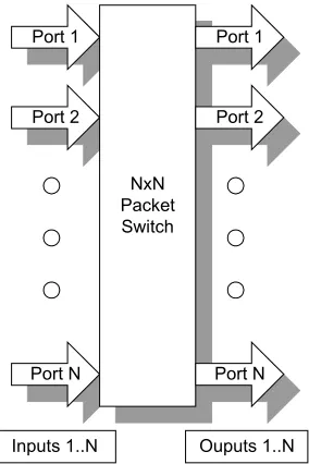
ports (large NxN). Figure 1.1 shows an example of a simple switch. The scalability of
conventional shared memory switches is largely limited by the following:
•
Centralized control for all of the stages.
•
Memory bandwidth is shared between ports.
•
Memory space is segregated.
The SW algorithm avoids Centralized control by having five independent pipeline
stages. These pipeline stages need only the information available locally. Having multiple
memory modules parallelizes memory bandwidth. This allows the packets arriving from
each port to be written simultaneously. Memory space is completely shared between all
ports, so there is more room to store large bursts of traffic. By avoiding the listed
limitations, the SW algorithm is better suited for scaling to larger NxN. The goal of this
research is not only to implement the SW switch algorithm in hardware, but to also predict
how large the SW algorithm can scale in modern hardware and what the hardware limitations
To understand fully how the SW algorithm will translate into hardware, it is best to
build a small working prototype, like a 4x4 switch. This is accomplished using an Altera
FPGA and Quartus II software for synthesis. This model is then used to determine what the
scalability bottlenecks and practicality issues would be for large NxN.
Port 1
Port 2
Port N
NxN Packet Switch
Inputs 1..N Ouputs 1..N
Port 1
Port 2
Port N
Figure 1.1 Example of a simple network Switch
1.1 Organization of the Thesis
Chapter 2 will briefly discuss several different network-switching algorithms and a brief
comparison to SW. Chapter 3 will outline my implementation of a 4x4 SW switch in an
FPGA with parameters
σ
= 12,
m
= 8, and
p
= 2. These parameters define the way the
memory is handled in the algorithm. This thesis will not go into great detail about the
algorithm. One is expected to reference Dr. Sanjeev Kumar’s work in [1] on this subject for
more information.
3
provide verification results on the hardware implementation of this 4x4 SW switch. Chapter
6 will provide conclusions that the research uncovered and what the future plans are for the
Chapter 2
Other Network Switch Architectures
Modern shared-memory switches such as presented in [2] employ centralized control.
They also must share memory bandwidth between ports. As port quantity increases, the
tasks that the controller must accomplish also increases. In addition, the memory bandwidth
that is shared between ports becomes a problem. These factors limit the scalability of this
switch architecture.
Some of these shared-memory switch architectures such as the one presented in [3]
distribute bandwidth among multiple memory modules. This architecture also employs a
centralized controller for all functions. As port quantity grows, so does the required memory
and therefore the length of the search through shared memory space. This architecture also
requires that the controller manage all stages of the switch. Read and write operations,
searches, and other functions grow as switch size grows. For these reasons, this architecture
is known to have limits on scalability.
To counteract this scalability problem, many smaller shared memory switches are
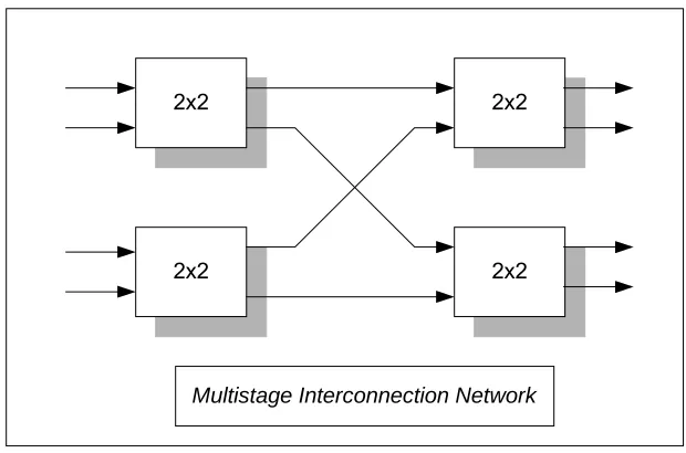
connected together to achieve a larger port quantity [4] such as in Figure 2.1. In this figure,
four 2x2 shared memory switches are connected together to achieve a 4x4 switch. This is
5
2x2
2x2
2x2
2x2
Multistage Interconnection Network
Figure 2.1 Example of a MIN
The hardware for these shared memory switch architectures is known not to scale much
larger than 16x16. Although a larger port quantity is achievable using MIN as mentioned
above, these packet switches are known to have poor throughput for high network traffic
loads. As an example, consider connecting multiple 8x8 shared memory packet switches in
MIN fashion to obtain a 64x64 packet switch. The 8x8 switch itself has a nearly linear
relation of traffic load versus throughput (Figure 2.2 from [1]). However, when it is grown
Figure 2.2 Nearly linear load is achieved with an individual 8x8 switch (from [1])
Figure 2.3 64x64 MIN based on the 8x8 shared memory switch (from [1])
7
memory modules. As a comparison, consider a 64x64 SW switch with the same buffer
capacity shown in Figure 2.4 from [1].
Figure 2.4 Load versus throughput for a SW switch (from [1])
For the same traffic and buffer memory, the SW architecture offers near-linear load versus
throughput. A throughput of almost 0.9 is achievable with this architecture. MIN plateaus
before 0.6 with traffic and memory being equal. SW offers significant improvements over
Chapter 3
Implementation
This thesis will not provide a review of the Sliding-Window (SW) switching
algorithm. An excellent explanation of this algorithm may be found in [1]. This chapter will
often reference this article to explain the architecture. The SW algorithm is a generic
switching algorithm that is independent of the type of packet. The overall function of this
algorithm is to queue and route a given packet to the specified output port.
3.1 Method
A software version of this algorithm was created in Matlab for debugging and
verification purposes. Matlab was chosen because of its excellent matrixing capabilities.
Performance of the Matlab comparison algorithm is also not really an issue since the HDL
version will be much slower.
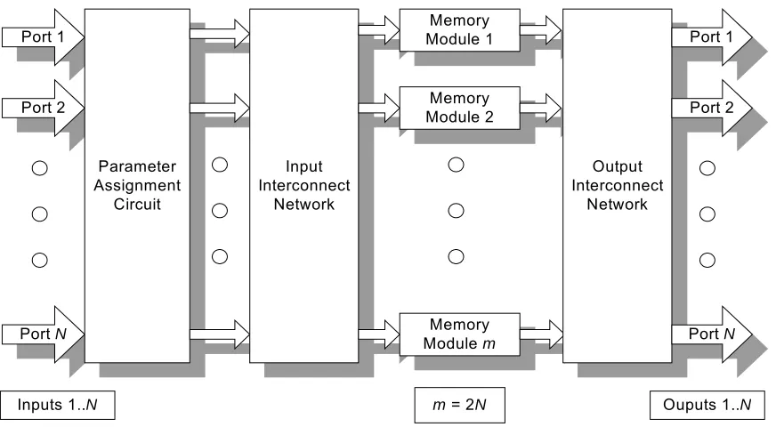
The overall structure of the algorithm, and the hardware, is shown in Figure 3.1.
Notice there are five distinct pipeline stages to the entire algorithm:
1. The Parameter Assignment Circuit (PAC)
2. The Input Interconnection Network (IIN)
3. The Read Operation (Memory Module input)
9
Port 1
Port 2
Port N
Parameter Assignment
Circuit
Input Interconnect
Network
Memory Module 1
Memory Module 2
Memory Module m
m = 2N
Output Interconnect
Network
Port 1
Port 2
Port N
Inputs 1..N Ouputs 1..N
Figure 3.1 Architecture of the Sliding-Window Switching Algorithm
Before the hardware can be designed, a certain set of assumptions must be founded.
They are as follows:
1. Design a 4 input, 4 output switch (
N
= 4)
2. The Packets are 64 bytes long.
3. The header (
d
) is in the first few bits.
4.
σ
= 12,
m
= 8,
p
= 2.
5. The data arrives serially and leaves serially.
6. The target hardware is the Altera EP20K400EFC672-3
The packet length of 64 bytes is the size of a standard ATM cell. The header is
assumed to contain
d
and is located in the first byte of the packet. Dr. Sanjeev Kumar
suggested that the parameters
σ
= 12,
m
= 8, and
p
= 2 be used for this design. For testing
has only 24 channels. Serial data for each port would require 4 inputs + 4 outputs + 1 clock
+ 1 reset = 10 channels. This is not including any debugging signals.
The Altera FPGA has certain limitations that must be considered. It has about 16,000
registers, but 239,000 bits of configurable RAM. This is important considering the packets
are 64 bytes (512 bits). The number of packets that must be stored are determined by the
parameters
σ
= 12 and
m
= 8 to yield:
bits
152
,
49
512
12
8
×
×
=
This large number of bits is too large to fit in the registers, but small enough to fit in the
RAM. To use the RAM and Registers efficiently, and to design hardware efficiently in
general, block diagrams of the hardware must be created before coding the HDL models.
The Altera FPGA must be programmed from a binary file created by the Quartus II
software. This software synthesizes the HDL to a binary that may be downloaded to the
FPGA. Quartus II supports several HDL’s, but I chose Verilog to implement this hardware
because of my familiarity with this language.
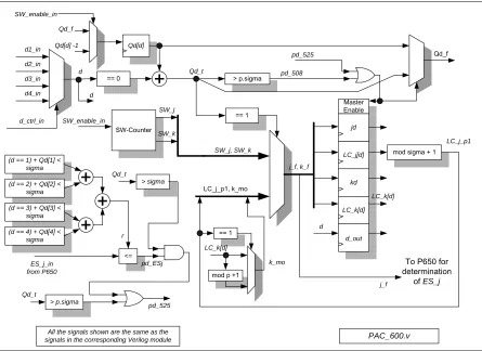
3.2 Parameter Assignment Circuit Design
The most challenging part of the entire SW algorithm to design in hardware is the
Parameter Assignment Circuit (PAC), which is the first stage of the switch. It contains
counters, variables, and tables that must be analyzed and updated accordingly. The PAC
assigns the self-routing parameters
i, j, k
to each packet. These parameters allow the packet
11
PAC core is broken down into two distinct sub-pipeline stages of processors (Processor 1 and
Processor 2). This is because the entire PAC, and therefore the pipeline, operates
sequentially on a given set of packets during a given switch cycle. The parameters assigned
to a packet have a direct dependency on previous packet assignments. This dependency
would be difficult, if not impractical to predict. This makes it extremely difficult to pipeline
or parallelize this parameter assignment hardware much further. The rest of the PAC is
designed around this Processor Core.
Processor 2 (P650)
FSM Control Signals
i, j, k, d d
Processor 1 (P600)
PAC Processor Core
j, k, d
Table Data
Figure 3.2 Parameter Assignment Circuit Core
P600 assigns the
j
and
k
parameters while P650 uses
j
and
k
to compute the
i
parameter. Both processors work together to handle queue control, although P600 does most
of this. The overall function of the PAC is read a packet from an input port, assign the
parameters, and repeat until all the packets on the input have been assigned. This process is
defined as one cycle. The PAC must store all the packets from the input each
switch-cycle as they arrive because it is a pipeline stage.
3.2.1 PAC Header Circuit design
It would be convenient to grab the
d
parameter out of the header as we parallelize the
extracts
d
at the earliest possible time. The FSM module,
PAC_NCFSM.v
, triggers this
capturing of
d
. The data parallelizing is done using a shift register macro created by the
Quartus II Mega-Function Wizard. This macro just uses registers, and not RAM, since there
is no way to bitwise shift the on chip RAM. It is created in the same way as the RAM is
using the Quartus II
Project Megafunction Wizard
. The shift register converts the 512 bits of
serial data to 8 x 64 bit words.
A block diagram of the hardware to create this module is shown in Fig. 3.3. There
are four of these modules in the upper-level design
PAC_Full.v
corresponding to each input
port. All the inputs and outputs of the modules are labeled with <signal>_in or <signal>_out.
In addition, <signal>_in will be connected to <signal>_out of the previous module. This is
done for clarity of signal flow. Another mantra used in this design is that algorithm variables
such as
d
are actually one extra bit longer than necessary. The reason for this is that all
algorithm counters and variables start at one. This allows the hardware to follow the
algorithm, which also starts at one, to avoid confusion. It also lets zero be the special case of
13
shift1
ser_in sp_out
64
3
d_out d_valid_in
F
S
M
C
ont
ro
l
S
ign
al
s
All the signals shown are the same as the signals in the
corresponding Verilog module PAC_Header.v
X 4
d_outFigure 3.3 The Header Module
3.2.2 PAC Memory design
Recall that PAC is a switch pipeline stage. This implies a one-packet delay each
switch cycle that must be implemented with some type of memory. So the PAC must store
the packet somewhere each cycle, preferably in RAM, otherwise 512 bits x 4 inputs = 2048
registers will be wasted. This RAM is created using the Quartus II
Project Megafunction
Wizard
just like the shift register in the header. This packet delay is handled by reading the
current write address plus one. Therefore, each memory writes (and reads) the packet in 8
cycles per switch cycle. The read address will read what is currently being written 8 memory
cycles (one switch cycle) later.
PAC_Memory.v
also handles injecting the newly assigned
i, j, k
parameters (from the
P650) back into the packet. Once the parameters are found, they are temporarily stored until
they can be injected into the packet at the right time using mux1 and the
ctrl1_in
signal from
the FSM. All control signals and addresses are handled by the FSM. The block diagram for
must be four of these connected to the
sp_out
output of each Header module. Please note
that the PAC memory module is not related to the Memory Modules involved in queuing in
the third and fourth pipeline stages.
Mux1 8 x 64 RAM(ram1)
i, j, k, d ijkd_valid_in
i_in, j_in, k_in, d_in
i, j, k, d
sp_in[12:0]
mux1_out
sp_in
64 52
13
64
addr_in
1
wren_in
ctrl1_in
addr_p1
FSM Control Signals
All the signals shown are the same as the signals in the
corresponding Verilog module PAC_Memory.v
sp_out
rd_addr wr_addr wren d
q
X 4
Figure 3.4 The PAC Memory Module
3.2.3 The PAC Finite State Machine
The PAC control signals are generated by one Finite State Machine (FSM), the
PAC_NCFSM.v
module. This module is simply a 9-bit counter that sends out control signals
based on the current counter values. The simplest way to accomplish control for many
events that are strictly time dependent, such as in the PAC, is just to use a counter and logic.
This is not a typical FSM because it has no inputs other than
clock
and a
reset
. However,
15
9-bit counterControl Logic
FSM Control Signals clock
counter
addr_out
ijkd_valid_out
PAC_NCFSM.v
Figure 3.5 The PAC Finite State Machine
3.2.4 PAC SW-Counter
Each processor has its own Sliding-Window Counter. This counter updates
according to the SW algorithm given in [1]. This counter is a two-digit modular counter that
updates when signaled by the FSM. The first digit is SW_j and increments mod
σ
. The
second digit,
SW_k,
increments mod
p
only when SW_j == 1. Recall that all algorithm
variables such as the Sliding-Window Counters
SW_k
and
SW_j
start at (reset to) one instead
of zero. This SW counter is what the
j
and
k
values are based on. It also determines when
portions of the tables are updated in both processors such as the Scan Table (
ST
) in P650. A
block diagram of this counter is shown in Figure 3.2.5. This diagram corresponds to the
SW_j
SW_k
++
==
==
p
1
== 1
1 2
0
0
0
1 1
1
All the signals shown are the same as the signals in the corresponding
Verilog module
PAC_SWCounter.v
Figure 3.6 The Sliding Window Counter
3.2.5 PAC Processor 1
The first stage of the PAC core is P600. This processor uses counters, tables, and
conditions to assign the parameters
j
and
k
. The design is relatively straightforward and
based on the flowchart given in Figure 3.7 from [1]. Most of this flowchart translates straight
into hardware easily.
17
and LC_k[d] are used to keep track of the previous
j and k
parameter assignments to a
particular output port
d
. Qd[d] is a queue counter that holds the number of packets destined
to the corresponding output port. All of the conditional dependencies for P600 allow the
entire
j, k
assignments and queue control to be easily completed in one clock (or packet)
cycle per packet. After all the packets have been assigned there is an update cycle triggered
by the FSM’s
SW_enable
signal. This update cycle increments the
SW_j
and
SW_k
counters
according to the SW scheme. It also simultaneously decrements the
Qd[d]
arrays that
contain the queue length for each port, because each port always removes a packet from the
Figure 3.7 Flowchart of P600 operations (Figure 5 from [1])
Step 524 is completed using the following pseudo code:
if (Qd > p. σ) drop the packet Qd = Qd - 1
19
ES_j
is a scalar that contains the number of empty slots in vector
ST[j]
and
r
is the
number of input ports that have queue lengths less than
σ
.
There is unfortunately a catch in the algorithm to hardware translation that makes one
small part, the
ES_j
calculation, not so straightforward.
ES_j
depends on the
j_524
vector of
the Scan Table:
ST[j_524].
Since
ST
is in P650,
ES_j
is calculated by P650 based on the
current
j_524
value from P600. This
ES_j
is then returned to P600, where P600 uses this to
decide whether to drop the packet. The reason this must be looped backwards in the pipeline
is because of the data dependency. This
ES_j
calculation depends on
ST[j_524]
which is
only in P650. In addition, P650 depends on the current
j
and
k
to update the
ST
in the next
packet cycle. However,
j
and
k
are not valid (i.e. they may be dropped) until
ES_j
is
calculated and compared in P600. So on top of having to loop this
ES_j
value backwards in
the pipeline from P650 to P600 we must also speculate when calculating
ES_j
what
ST[j_524]
will be after P650 updates with the current
j, k values
. Please note that
j
is the
same as
j_524
delayed by a cycle (and dropped if it fails 524 or 508). Also, j_524 affects no
other decisions or registers in P650 directly in this calculation. The
ES_j
calculation is
essentially an isolated circuit in P650 that reads the Scan Table. The hardware block diagram
of P600 is displayed in Figure 3.8.
Note that there is only one P600 per switch. The reason this is so is because the
algorithm depends heavily on the previous packet’s parameters. This dependency makes it
difficult to assign these parameters any other way than sequentially. Since the assignment is
sequential, only one processor is needed per switch to assign
j
and
k
. The same is true for
Master Enable == 1 d2_in d1_in d3_in d4_in d d_ctrl_in == 0 Qd[d] > p.sigma == 1 pd_508 SW_j, SW_k jd LC_j[d] kd LC_k[d] d_out j_f, k_f
mod sigma + 1 LC_j_p1
LC_j_p1, k_mo
LC_k[d]
LC_k[d]
mod p +1
k_mo Qd_f
pd_525 Qd_t
To P650 for determination
of ES_j Qd_f
(d == 1) + Qd[1] < sigma (d == 2) + Qd[2] <
sigma (d == 3) + Qd[3] <
sigma (d == 4) + Qd[4] <
sigma r <= ES_j_in from P650 > sigma Qd_t > p.sigma Qd_t pd_525 pd_ESj d SW_enable_in Qd[d] -1
All the signals shown are the same as the
signals in the corresponding Verilog module PAC_600.v SW-Counter SW_enable_in SW_j SW_k d j_f
Figure 3.8 P600 design
3.2.6 PAC Processor 2
The second stage of the Processor pipeline is P650. This processor’s main duty is to
assign the
i
parameter. It also maintains the Scan Table
ST
and calculates
ES_j
for P600
based on the current j_524 value.
ST
is a two-dimensional table (
j
,
i
) that holds the
k
values
for the previously assigned packets. This table’s purpose is to make sure P650 writes the
21
of clearing all the
k
’s stored in vector
ST[SW_j_addr]
that are the same as the
SW_k
value.
This corresponds to reading out a packet from the memory to the output port. This
SW_j,
SW_k
value matches the three-switch cycle delayed value of the counter in the memory
Read-Out operation (discussed later). The block diagram of the update hardware for P650 is
shown in Figure 3.9. Recall that all algorithm variables such as
SW_j
and
SW_k
start at one
and hardware such as RAM starts at zero. To bridge this gap the equivalent hardware
address is calculated by subtracting one from the SW algorithm variable. The resulting
Master Enable SW_Enable == SW_k == SW_k == SW_k == SW_k == SW_k == SW_k == SW_k
== SW_k ST[ { SW_j_addr, 0 } ] ST[ { SW_j_addr, 1 } ]
ST[ { SW_j_addr, 2 } ]
ST[ { SW_j_addr, 3 } ]
ST[ { SW_j_addr, 4 } ]
ST[ { SW_j_addr, 5 } ]
ST[ { SW_j_addr, 6 } ]
ST[ { SW_j_addr, 7 } ]
0 0 0 0 0 0 0 0 q0 q1 q2 q3 q4 q5 q6 q7 q0 q1 q2 q3 q4 q5 q6 q7 Master Enable
temp_i[ 0 ]
temp_i[ 1 ]
temp_i[ 2 ]
temp_i[ 3 ]
temp_i[ 4 ]
temp_i[ 5 ]
temp_i[ 6 ]
temp_i[ 7 ] SW_Enable 0 0 0 0 0 0 0 0 SW-Counter SW_enable_in SW_j SW_k -1 -1 SW_j_addr SW_k_addr
All the signals shown are the same as the
signals in the corresponding Verilog module Update hardware forPAC_650.v
Figure 3.9 Update Hardware for P650
P650 must find an empty slot in the
ST[j_addr]
vector, and assign the parameter
i
to
this location. There is also another algorithm to hardware translation problem here. Each
23
must also be doubled for this purpose of writing two packets simultaneously. The good news
is that the larger the switch is (in port quantity), the less likely this is to happen. Also the
chance of more than two packets requiring the same
i
value for a 4x4 switch is less than one
in ten million [11].
To avoid a duplicate
i
value, a register
temp_i
is used to hold the previous
i
assignments for the current switch cycle. This
temp_i
register has
m
bits, or a bit for each
Memory Module. This register is compared with
ST[j]
using a bitwise OR. Then this output
is searched bit by bit for an open or zero slot. A search implies a priority encoder in
hardware. The register is cleared at the end of every switch cycle.
The output of the bitwise OR operation mentioned above is the select-line for the
priority encoder
PE1
. Note that the select line of PE1 and PE2 can be thought of as inverted,
so that the first “0” slot is found instead of the first “1” slot. The inputs to the priority
encoder are hard-wired numbers corresponding to each priority encoder input number (see
Figure 3.10). For this switch, there are 8 select lines and 9 sets of inputs. Note that one of
the inputs to the priority encoder is the number 8 and specifies the default case, or an
unsuccessful search. The priority encoder finds the first empty (zero) slot (starting with the
MSB) on the select line and outputs the corresponding input, which has the corresponding
i
location. Since the MSB has highest priority,
temp_i
and
ST[j_addr]
are flipped bitwise in
the actual hardware implementation to match the SW algorithm. This flipping is arbitrary
4
_
1
8
,
7
,
6
,
5
,
4
,
3
,
2
,
1
_
1
11101010
_
_
1
11101010
])
_addr
[
(
|
)
_
(
10000000
_
11101010
]
_addr
[
=
=
=
=
=
=
output
PE
inputs
PE
line
select
PE
j
ST
i
temp
i
temp
j
ST
If an
i
cannot be located in this first search, a second
i
search is performed
simultaneously with
PE2,
which is another priority encoder. This search is only done on the
ST[j_addr]
vector. The result of this search is used only when the first search fails, which
means this must be a duplicate
i
value. The block diagram of the
i
assignment hardware for
25
Master EnableEnable
Master Enable
> 0 != 8
++ Master Enable == 8 == 0 == 0 == 0 == 0 == 0 == 0 == 0 == 0
All the signals shown are the same as the signals in the corresponding Verilog module
i assignment for PAC_650.v
ST[ { j_addr, 0 } ]
ST[ { j_addr, 1 } ]
ST[ { j_addr, 2 } ]
ST[ { j_addr, 3 } ]
ST[ { j_addr, 4 } ]
ST[ { j_addr, 5 } ]
ST[ { j_addr, 6 } ]
ST[ { j_addr, 7 } ]
temp_i[ 0 ]
temp_i[ 1 ]
temp_i[ 2 ]
temp_i[ 3 ]
temp_i[ 4 ]
temp_i[ 5 ]
temp_i[ 6 ]
temp_i[ 7 ]
PE2 1 0 2 3 5 4 6 7 i_addr2 PE2 1 0 2 3 5 4 6 7 i_addr1 8 8 j_out k_out i_out d_out i_addrf i_addrf d_in Enable Enable i_addrf 1 i_addrf k_in d_in k_in j_in Master Clear == 0 d_in j_in -1 j_addr
Figure 3.10 Parameter
i
assignment for P650
P650 must also use
ST
to calculate the
ES_j
value for P600 based on
j_524. ES_j
holds the number of empty slots in the
ST[j_524_addr]
vector (which holds the
k
values of
the packets in the
j_524_addr
vector). To calculate
ES_j
, a comparator is used on each of the
all the
k
values for the
j
thindex of all the Memory Modules
.
The results of these comparators
are added together to obtain
ES_j
. If the
j_524_in
is equal to the current
j_in
value then we
must speculate that
ES_j
is actually
ES_j
- 1. This is because the parameters
j
and
k
on the
input have not been written to the
ST
yet. If it has the same
j
as the
j_524
(the future packet)
then we must speculate that this packet occupies a slot in the
ST[j].
This is not the case yet
because of the pipeline, as stated earlier. The way to get around this problem is to subtract
one from
ES_j
after the calculation. In summary P650, and therefore
ST,
can be thought of as
a cycle behind P600 because of the pipelining of these two processors. P600 needs data that
is effectively a cycle behind and must use informed speculation to access this data. A block
diagram of this calculation hardware is shown in Figure 3.11.
ST
is a two-dimensional table indexed by (
j, i
). This is implemented in hardware
using register based RAM, since it is relatively small. The address to one-dimensional RAM
is calculated by concatenating the
j
and
i
address bits. This effectively creates an efficient
two-dimensional address space assuming
i
(the lower bits of the address) has a maximum
value that is a power of 2 minus 1 such as 7 = 2
3- 1.
For example if j = 5 and i = 2 then the address {j_addr, i_addr} in binary is:
27
j_524_in
-1 j_524_addr
ST[ { j_524_addr, 0 } ]
ST[ { j_524_addr, 1 } ]
ST[ { j_524_addr, 2 } ]
ST[ { j_524_addr, 3 } ]
ST[ { j_524_addr, 4 } ]
ST[ { j_524_addr, 5 } ]
ST[ { j_524_addr, 6 } ]
ST[ { j_524_addr, 7 } ]
== 0
== 0
== 0
== 0 == 0
== 0
== 0
== 0
ES_temp1
== > 0
j_in j_524_in
ES_j
All the signals shown are the same as the signals in the corresponding Verilog module
ES_j calculation hardware for
PAC_650.v
Figure 3.11
ES_j
calculation in hardware
3.2.7 PAC Top Level Design
All of the hardware modules are assembled at the top level to create the PAC.
This top-level assembly only consists of modules and wires and is straightforward to derive
from the individual modules and their signals. The overall block diagram for this hardware is
P600
FSM
Header4 Header3 Header2 Header1
Memory2 Memory1
Memory3
Memory4 P650
ser_in[1]
ser_in[2]
ser_in[3]
ser_in[4]
sp_out1
sp_out2
sp_out3
sp_out4
All the signals shown are the same as the signals in the corresponding Verilog module
Top Level Module PAC_Full.v
sp
sp sp
sp
d d
d d
j, k
i, j, k ES_j
Figure 3.12 Top Level Assembly of the PAC
3.3 Input Interconnection Network Design
The Input Interconnection Network (IIN) is the second stage of the pipeline. The
main task for this stage of the SW algorithm is to route the packets from each of the four
PAC_Memory.v
modules to one of the eight Memory Modules specified by the packet’s
i
parameter. This routing is complicated by the fact that on rare occasions there may be a
29
The packet datapath of the PAC is 64 bits. This datapath size, while not a problem in
PAC, poses a problem for the crossbar. The reason is that the crossbar must switch a 64 bit
wide datapath. A datapath this wide creates unnecessarily large logic in the crossbar. This
size is arbitrary and could be reduced to a 1 bit wide datapath. However, it is best to choose
a size that can be written to the Memory Module RAM easily. The size that I decided on was
8 bits. To accomplish this datapath conversion, a module was created that does this and
extracts the
i
value for routing.
3.3.1 IIN Header Module
The IIN Header Module,
IIN_H.v
, converts the datapath from 64 to 8 bits and extracts
the
i
parameter value. It also introduces the pipeline delay the same way that the PAC does:
by using 2048 bits of on chip RAM. The same Quartus II generated RAM macro is used to
accomplish this as in PAC.
This module uses the control signals generated by a Finite State Machine. This FSM
generates all the controls and addresses for each module in the IIN. As the first 64 bits of a
packet arrives, the IIN Header Module stores it in the on chip RAM. This word is then read
out eight cycles later. The whole word at the output of the RAM is addressed using a mux to
select 8 bits at a time. The 8 bit group assigned to
ps_out
. Simultaneously the
i
value is
extracted for routing the packet to the appropriate Memory Module. The hardware for this
8 x 64 RAM (ram1) sp_in
addr_in
1
wren
addr_p1
All the signals shown are the same as the signals in the
corresponding Verilog module IIN_H.v
rd_addr wr_addr wren d
q
X 4
64
ps_addr_in ps_out
FSM Control Signals
ps_conv
id
ijkd_en_in
id
64
Figure 3.13 IIN Header Module Diagram
3.3.2 IIN Crossbar
The main task of the Input Interconnection Network is to route a packet to the
appropriate Memory Module. When there are no destination conflicts this can be
accomplished with a crossbar. There are multiple ways to implement a crossbar as suggested
in [5]. Three of the ways that may be implemented in this FPGA are:
1. A mux for each output
31
The RAM crossbar method unfortunately will not work in parallel like the other two
methods. While using Tristate buffers is possible, the simplest way is to just use muxes.
As stated earlier, a crossbar works best when there are no destination conflicts. But,
this is not the case with this design. The destination conflict is fortunately predictable in that
the design only needs to handle a destination conflict of two. The algorithm also requires
that when there is a destination conflict, the two packets need to be written simultaneously to
the same Memory Module in the same switch cycle. This is accomplished by doing the
normal writes (no destination conflicts) to the memory modules at half the bus speed. When
there is a conflict the crossbar toggles between the two packets while the Memory Module
writes these two packets to their appropriate location at the normal bus speed.
This design uses priority encoders (PE’s) for this task instead of muxes to implement
a crossbar. PE’s are used in this design because they perform a sequential search, and
therefore chooses the first input with a matching
i
value. There are two priority encoders at
each output. Each priority encoder performs its “search” in opposite directions. In the case
of duplicate
i
values, there will be different packet data on each PE. A mux selects between
these two PE’s to do the final stage of routing. Most of the time, this mux just selects the
first (main) PE. However, when there is a duplicate
i
value, the mux toggles between the
main PE and the secondary PE to write both packets simultaneously. Note that the mux
could perform this toggle all the time and work correctly (because both PE’s will have
identical output), but I chose only to toggle in the case of duplicate
i
values. This toggle
signal is actually generated by the Memory Module in response to the duplicate
i
signal,
i_dupl_out
from the IIN Crossbar Module. The diagram that corresponds to this module is
There is one IIN Crossbar Module,
IIN_CB.v,
connected to each Memory Module.
So in this 4x4 switch there will be 8
IIN_CB.v
’s.
Reverse bit order
jd1_in, kd1_in, p1_in
jd2_in, kd2_in, p2_in
jd3_in, kd3_in, p3_in
jd4_in, kd4_in, p4_in
jd_tmp, kd_tmp, line_tmp
jd1_in, kd1_in, p1_in
jd2_in, kd2_in, p2_in
jd3_in, kd3_in, p3_in
jd4_in, kd4_in, p4_in
jd_dupl, kd_dupl, line_dupl
jd_out, kd_out, line_out
toggle_dupl_out ctrl_in
ctrl_in_f FSM Control
Signals
Sum all
bits > 1
ctrl_in i_dupl_out
33
3.3.3 IIN Finite State Machine
Part of the IIN contains a Finite State Machine (FSM) that is modeled after the one in
the PAC. It contains a counter and output logic based on the counter to generate addresses
and control signals.
There is also extra combinational logic that generates control signals for the Crossbar
Modules based on the
i
parameters. Eight control signals, one for each Memory Module, are
generated based on the four
i
parameters from the Header modules. These control signals are
select lines that controls the actual routing done by the PE’s in the Crossbar Module. The
hardware block diagram for this module is shown in Figure 3.15.
The control signals are generated by first sending each of the four
i
values from each
Header Module to a mux. This mux selects a one-hot 8-bit binary number corresponding to
the
i
value. This 8-bit number is divided bitwise so that one bit from each port goes to each
of the eight Crossbar Modules. Since there are four inputs, there are four bits total going to
each Crossbar Module. This is another one-hot (except when
i
is duplicated) signal for the
two PE’s in each Crossbar Module. As an example, consider the following:
Notice the control signal
ctrl5_out
has two bits hi (which means there are duplicate
i’s)
. This is OK because it is the select line for a priority encoder, which simply searches the
select line for the first hi bit. This signal is also flipped bitwise and sent to the second
priority encoder in the Crossbar Module. In this case, the main and secondary PE will select
different ports. The Crossbar Module detects this and reacts accordingly so that both packets
are sent to the Memory Module simultaneously, in an interleaved fashion.
This FSM module contains more than just an FSM. This logic, although not state
dependent, had to go somewhere central to the IIN. The FSM is the only single module in
the IIN and was therefore the most logical choice.
35
WireRegrouping
9-bit counter ControlLogic
FSM Control Signals clock counter addr_out ijkd_en_out IIN_FSM.v All the signals shown are the same
as the signals in the corresponding Verilog module 00000000 10000000 01000000 00100000 00001000 00010000 00000100 00000010 00000001 c1 id_in1 00000000 10000000 01000000 00100000 00001000 00010000 00000100 00000010 00000001 c2 id_in2 00000000 10000000 01000000 00100000 00001000 00010000 00000100 00000010 00000001 c3 id_in3 00000000 10000000 01000000 00100000 00001000 00010000 00000100 00000010 00000001 c4 id_in4 ctrl1_out ctrl2_out ctrl3_out ctrl4_out ctrl5_out ctrl6_out ctrl7_out ctrl8_out
3.3.4 IIN Top Level Implementation
The upper level IIN design contains one FSM Module, eight Crossbar
Modules, and four Header Modules. All of these hardware modules are assembled at the top
level to create the IIN. This module assembly occurs in the file
IIN.v
. The overall block
diagram for this hardware is shown in Figure 3.16. Some signals, such as
jd_out1..8
, are not
37
FSMHeader4 Header3 Header2 Header1
Crossbar1
port1_in
port2_in
port3_in
port4_in
line1_out
All the signals shown are the same as the
signals in the corresponding Verilog module Top Level Module IIN.v
Crossbar2 line2_out
Crossbar4 line4_out
Crossbar3 line3_out
Crossbar5
line5_out
Crossbar6 line6_out
Crossbar8 line8_out
Crossbar7 line7_out
i1 i2 i3 i4 pack
e
t
da
ta
pac
ket
da
ta
pack
e
t
da
ta
pa
ck
et
da
ta
Figure 3.16 IIN Top Level Design
3.4 Memory Module Design
So far, the first two stages have been single pipeline stages. This section of the
switch actually makes up two pipeline stages. They are the write and read operations, which
make up the third and fourth stages of the pipeline respectively. Except for handling the
3.4.1 Memory Module Write Operation
The write operation takes place in the Memory Module RAM file
MM_RAM.v
.
Recall that the data is arriving in 8-bit words from the IIN Crossbar Module. Since a packet
is 64 bytes and sigma = 12, there are 64 x 12 = 768 bytes per Memory Module RAM. There
are eight Memory Module RAMs so there are 6144 bytes of RAM in the Memory Module
top-level design. The
j
and
k
parameters for an arriving packet have already been extracted
in the previous stage (IIN) and are present at each Memory Module RAM input along with
the data. This is crucial so that the data may be written immediately. The write depends
heavily on the
j
parameter because it points to the slot in the Memory Module that the packet
is assigned.
If
the
i_dupl_in
signal is raised, then the Memory Module RAM responds by toggling
the
toggle_dupl_out
signal. This tells the crossbar to toggle between the main and secondary
packet if there is a duplicate
i
parameter for the packets. Toggling between the packet and
parameters interleaves the two packets together in one write. Please note that the normal
write cycle has been doubled to accommodate this rare occurrence of duplicate
i
parameters.
A write is triggered when a packet arrives. The write address is calculated from an
address generated internally by an accumulation register,
w_addr_reg
, as the lower bits
concatenated with the
j_addr
. The lower bit of the
w_addr_reg
is the
toggle_dupl_out
signal. The upper eight bits are used in the write address generation. The Output Scan Array
39
3.4.2 Memory Module Read Operation
The read operation is triggered by the Memory Module FSM. The read address is
then internally generated by an accumulation register,
r_addr_reg
, concatenated with
SW_j_addr
. Packet data is not sent out unless the
k
parameter in the
SW_j
slot of the OSA
matches the current
SW_k
value. The diagram for this hardware is shown in Figure 3.17.
Consider the case of reading an address that is currently being written. This could
cause a conflict and incorrect data. To avoid this conflict, time may be inserted between the
writes so that the data can be read. Another way to avoid this conflict is to simply stagger the
read and write addresses so that the reads are one address behind the writes. Inserting time
between writes seemed to be the simplest way, since there is plenty of time in this design to
spare. Sufficient time also already existed between the writes. So eight bytes are written,
and then eight bytes are read. This is repeated eight times until the entire 64-byte packet is
-1 -1
read_en_d
++
96 x 8 RAM line_in
w_addr_reg[8:1]
All the signals shown are the same as the signals in the
corresponding Verilog module MM_RAM.v
rd_addr wr_addr wren d
q
X 8
8
FSM Control Signals ps_conv
8
w_addr_reg
OSA Enable
pkt_here_in pkt_here_in
0
update_in
kd
==
SW_k
OSA[SW_j_addr]
SW_j_addr jd_addr
read_en_d
pkt_here_out pkt_here_out
0
++
r_addr_reg 0
update_in pkt_here_in
read_en_in
read_en_in read_data_out
jd
SW_j
update_in jd_addr
r_addr_reg
SW_j_addr
41
3.4.3 Memory Module FSM
The Memory Module FSM is, like the FSM in the PAC, a counter with output logic.
This FSM has a delay register that applies a three switch-cycle delay to the local
SW-Counter. This three switch-cycle delay is a bit tricky to derive from the HDL file
MM_FSM.v
or the block diagram (Figure 3.18) because it looks like a two cycle delay. The
delay register goes high on the 1
stclock cycle of the third switch-cycle. However, the
update
signal does not go high until the beginning of the fourth cycle. The reason there is a delay
here is because
delay
will not make its transition until
counter[8:0] = 1
, but
update
needs
counter[8:0] to be 0:
update = (delay && (counter[8:0] == 9'h000));
The
delay
register is used as a flag to signal that two switch cycles have taken place. The
update
signal, which is based on the
delay
register, is used to update the SW-Counter among
other tasks. Since there are three pipeline stages before the Read Operation, the SW-Counter
needs to be three cycles behind in the Memory Module. The Memory Module Read
==2
11-bit counter ControlLogic
FSM Control Signals
clock
counter
update
read_en_out
delay
All the signals shown are the same as the signals in the
corresponding Verilog module MM_FSM.v
counter[10:9]
Figure 3.18 MM FSM Design
3.4.4 Memory Module Top-Level Design
The Top-Level implementation of the Memory Section consists of an FSM, eight
43
Memory Module8
duplicate i control line_in8
Memory Module7
duplicate i control line_in7
Memory Module6 Memory Module5
duplicate i control line_in5
Memory Module4
duplicate i control line_in4
SW-Counter
update_in
SW_j
SW_k
FSM Module1Memory
out1
All the signals shown are the same as the signals in the corresponding Verilog module
Top Level Module MM.v Memory Module2 out2 out4 Memory Module3 out3 out5 out6 out8 out7
duplicate i control line_in1
duplicate i control line_in2
duplicate i control line_in3
duplicate i control line_in6 SW_j, SW_k SW_j, SW_k SW_j, SW_k SW_j, SW_k SW_j, SW_k SW_j, SW_k SW_j, SW_k SW_j, SW_k
Figure 3.19 Top Level Memory Module Design
3.5 Output Interconnection Network
This stage of the pipeline actually does not introduce any type of delay, because it is
their respective
d
parameter. There can be no destination conflicts in this stage because the
algorithm takes care of this problem.
When packet data arrives, the first byte contains the
d
parameter. This parameter is
stored for the duration of the packet data and is simultaneously used to route the packet to its
destination port.
The routing for this stage of the switch is done by a crossbar similar to the one in the
IIN. The
d
parameter selects a one-hot signal from a mux. This signal is regrouped in a
similar way to how the IIN regroups its one-hot signal. The regrouped signal is sent to a
priority encoder at the destination port. The destination port is then connected to the
45
WireRegrouping
OIN.v
All the signals shown are the same as the signals in the corresponding Verilog module
0000 1000 0100 0010 0001 c1 dd1_f ctrl1
ctrl2 ctrl3 ctrl4
0000 1000 0100 0010 0001 c2 dd2_f 0000 1000 0100 0010 0001 c3 dd3_f 0000 1000 0100 0010 0001 c4 dd4_f 0000 1000 0100 0010 0001 c8 dd8_f 0000 1000 0100 0010 0001 c7 dd7_f 0000 1000 0100 0010 0001 c6 dd6_f 0000 1000 0100 0010 0001 c5 dd5_f line_in1..8 line_in1..8 line_in1..8 line_in1..8 out_port3 out_port4 out_port1 out_port2
Figure 3.20 OIN Design
3.6 Parallel-Serial Conversion
This part of the design is required only for actually viewing the output data in the
FPGA design. It is attached to the output of the OIN. As stated earlier in this chapter, there
are only 24 channels on the Data Acquisition Card. One way to obtain the packet data is to
serialize it so that the number of output ports is minimized to four one-bit ports. There are
other ways of doing this such as time-sharing a bus between output ports, but serialization is
This converter acts as a 64-bit buffer to store the data as it arrives. Serialization is
accomplished by writing the arriving packet data to a bank of bit addressable RAM (see
Figure 3.21). This RAM is not precompiled on-chip RAM, but just a bank of registers. It is
written a byte at the time, but is read a bit at a time. Timing is key for this operation so a
9-bit counter is used. This stage is not part of the SW algorithm.
ps1
9-bit Counter Logic
line1_in
8
1
port1_out
ps4
Logic
line4_in
8
1
port4_out
PS.v
![Figure 2.3 64x64 MIN based on the 8x8 shared memory switch (from [1])](https://thumb-us.123doks.com/thumbv2/123dok_us/1487830.1182029/16.612.92.371.73.296/figure-x-min-based-x-shared-memory-switch.webp)
![Figure 2.4 Load versus throughput for a SW switch (from [1])](https://thumb-us.123doks.com/thumbv2/123dok_us/1487830.1182029/17.612.102.453.134.399/figure-load-versus-throughput-sw-switch.webp)
![Figure 3.7 Flowchart of P600 operations (Figure 5 from [1])](https://thumb-us.123doks.com/thumbv2/123dok_us/1487830.1182029/28.612.96.374.77.499/figure-flowchart-p-operations-figure.webp)