University of Windsor University of Windsor
Scholarship at UWindsor
Scholarship at UWindsor
Electronic Theses and Dissertations Theses, Dissertations, and Major Papers
2008
A Compact Camera with a Reconfigurable Real-time Embedded
A Compact Camera with a Reconfigurable Real-time Embedded
Image Processor for Pharmaceutical Capsule Inspections
Image Processor for Pharmaceutical Capsule Inspections
Anthony Karloff
University of Windsor
Follow this and additional works at: https://scholar.uwindsor.ca/etd
Recommended Citation Recommended Citation
Karloff, Anthony, "A Compact Camera with a Reconfigurable Real-time Embedded Image Processor for Pharmaceutical Capsule Inspections" (2008). Electronic Theses and Dissertations. 8030.
https://scholar.uwindsor.ca/etd/8030
A C o m p a c t C a m e r a with a Reconfigurable
Real-time E m b e d d e d Image Processor for
P h a r m a c e u t i c a l Capsule Inspections
by
Anthony Karloff
A Thesis
Submitted to the Faculty of Graduate Studies through
Electrical and Computer Engineering in Partial Fulfillment
of the Requirements for the Degree of Master of Applied Science at the
University of Windsor
1*1
Library and Archives CanadaPublished Heritage Branch
395 Wellington Street Ottawa ON K1A0N4 Canada
Bibliotheque et Archives Canada
Direction du
Patrimoine de I'edition
395, rue Wellington Ottawa ON K1A0N4 Canada
Your file Votre reference ISBN: 978-0-494-47052-7 Our file Notre reference ISBN: 978-0-494-47052-7
NOTICE:
The author has granted a non-exclusive license allowing Library and Archives Canada to reproduce, publish, archive, preserve, conserve, communicate to the public by
telecommunication or on the Internet, loan, distribute and sell theses
worldwide, for commercial or non-commercial purposes, in microform, paper, electronic and/or any other formats.
AVIS:
L'auteur a accorde une licence non exclusive permettant a la Bibliotheque et Archives Canada de reproduire, publier, archiver,
sauvegarder, conserver, transmettre au public par telecommunication ou par Plntemet, prefer, distribuer et vendre des theses partout dans le monde, a des fins commerciales ou autres, sur support microforme, papier, electronique et/ou autres formats.
The author retains copyright ownership and moral rights in this thesis. Neither the thesis nor substantial extracts from it may be printed or otherwise reproduced without the author's permission.
L'auteur conserve la propriete du droit d'auteur et des droits moraux qui protege cette these. Ni la these ni des extraits substantiels de celle-ci ne doivent etre imprimes ou autrement reproduits sans son autorisation.
In compliance with the Canadian Privacy Act some supporting forms may have been removed from this thesis.
Conformement a la loi canadienne sur la protection de la vie privee, quelques formulaires secondaires ont ete enleves de cette these.
While these forms may be included in the document page count,
their removal does not represent any loss of content from the thesis.
Canada
Bien que ces formulaires
© 2008 Anthony Karloff
Declaration of
Co- Authorship/Previous
Publication
I. Co-Authorship Declaration
This thesis also incorporates the outcome of a joint research undertaken in collab-oration with Neil Scott and Mohammad Islam under the supervision of Dr. Roberto Muscedere and Dr. Majid Ahmadi. The collaboration is covered in Chapter 2 of the thesis. In all cases, the key ideas, primary contributions, experimental designs, data analysis and interpretation, were performed by the author.
I am aware of the University of Windsor Senate Policy on Authorship and I certify that I have properly acknowledged the contribution of other researchers to my thesis, and have obtained written permission from each of the co-author(s) to include the above material(s) in my thesis.
DECLARATION OF CO-AUTHORSHIP/PREVIOUS PUBLICATION
II. Declaration of Previous Publication
This thesis includes one original paper that has been previously published in a peer reviewed journal, as follows:
Thesis Chapter
Chapter 2
Full Citation
A. Karloff, N. Scott, and R. Muscedere. A flexible design for a cost effective, high-throughput inspec-tion system for pharmaceutical capsules. In Proc. IEEE International Conference on Industrial Technol-ogy, April 2008
Status
Published
I certify that I have obtained a written permission from the copyright owner(s) to include the above published material(s) in my thesis. I certify that the above material describes work completed during my registration as graduate student at the University of Windsor.
I declare that, to the best of my knowledge, my thesis does not infringe upon anyones copyright nor violate any proprietary rights and that any ideas, techniques, quotations, or any other material from the work of other people included in my thesis, published or otherwise, are fully acknowledged in accordance with the standard referencing practices. Furthermore, to the extent that I have included copyrighted material that surpasses the bounds of fair dealing within the meaning of the Canada Copyright Act, I certify that I have obtained a written permission from the copyright owner(s) to include such material(s) in my thesis.
Abstract
The following thesis presents the system requirements, design methodology, final hardware design and system integration of a custom digital camera for high-speed pharmaceutical capsule inspections.
The primary goals of the camera design were to minimize the cost of the device and to have a flexible design that could be easily upgraded in the future. For this application, a 3.1 mega pixel CMOS image sensor was used with a USB 2.0 interface. In addition, the custom camera can pre-process image data in an embedded, recon-figurable real-time image processor implemented in a FPGA. All data processing in the camera occurs with only buffering four rows of an image, eliminating the need for RAM on the device and lowering the overall cost.
Acknow ledgments
Contents
Declaration of Co-Authorship/Previous Publication iv
Abstract vi
Dedication vii
Acknowledgments viii
List of Figures xiii
List of Tables xv
List of Abbreviations xvii
1 Introduction 1
1.1 Project Overview 2 1.2 Quality Control of Two Part Gelatin Capsules 2
1.3 Methods of Defect Detection 3 1.3.1 Current Inspection Methods 3
1.3.2 Introduction to Machine Vision 5
1.3.3 Commercial Systems 6
1.5 Thesis Organization 7
2 System Overview 9
2.1 Introduction to the Optisorter 9 2.1.1 Background Information 9 2.1.2 Summary of Operation 10
2.2 System Timing 11 2.3 Imaging Environment 13 2.4 Objectives for Modification 13
2.4.1 Selecting a Camera 14 2.4.2 Modifying the Imaging Environment 16
2.5 Proposed Design 18
3 Camera Design Methodology 21
3.1 Camera Design Flow 21 3.2 Design Specifications 23 3.3 Major Design Methods 23
3.3.1 Reconfigurable Hardware Programming 24
3.3.2 Simulation Tools 24 3.3.3 Prototyping Hardware 25
3.4 Testing 25
4 Hardware Design 26
4.1 Component Selection 26 4.1.1 Imaging Sensors 27 4.1.2 Reconfigurable Devices 28
4.2 Circuit Schematics 32 4.2.1 Micron MT9T001 CMOS Imaging Sensor 32
4.2.2 Xilinx Spartan-3E500 FPGA 33 4.2.2.1 I/O Connections 33 4.2.2.2 Clock Connections 34 4.2.2.3 Power Connections 34
4.2.3 TPS Triple Supply 35 4.2.3.1 Limiting Buck Converter Current 36
4.2.3.2 Setting VCCO 37 4.2.3.3 Sizing Soft Start Capacitors 37
4.2.4 Cypress FX2 USB Microcontroller 38
4.2.5 I2C Communication Bus 39
4.3 PCB Layout 40 4.3.1 PCB specifications 41
4.3.2 Component Placement 43 4.3.3 Power and Grounding 46 4.3.4 Bypass capacitors 47
4.3.5 Routing 51 4.3.6 Manufacturing Files 52
5 HDL Blocks and Programming 54
5.1 FPGA Programming Overview 54 5.2 Frame Timing and Data Synchronization 55
5.3 I2C Write Slave 57
5.3.1 I2C Bus Overview 58
5.3.2 I2C Slave VHDL implementation 59
5.5 Output Controller 62 5.6 Image Processing Block 64
5.7 Trigger Delay 65 5.8 Synthesis Constraints and Results 65
6 Image Processing 68
6.1 Demosaicking 68 6.2 Hardware Implementations 71
6.3 Edge-Enhanced Real-Time Hardware Demosaicking 73
6.4 Implementation and Results 77
7 Conclusion 79
7.1 System Integration 79
7.2 Summary 82 7.3 Future Work 84
References 86
A System Requirements 88
B Camera Board Schematics 92
C V H D L Code 99
D MATLAB Code 124
List of Figures
1.1 Typical Defects in Gelatin Capsules 4
2.1 Optisorter External View 10 2.2 Quadrant 1 Detailed 12 2.3 Camera Configuration 14 2.4 System Block Diagram 18 2.5 Camera Block Diagram 19 3.1 Hardware Design Flow 22 4.1 DCM with Off-Chip Delay Feedback 35
4.2 PCB Design Flow 41 4.3 PCB Partitions and Final Layout 44
4.4 PCB Power Plane Layout 47 4.5 Bypass Capacitor Values 48 4.6 Bypass Capacitor Impedance Profile [1] 48
4.7 Capacitor Placement Inductive Loop[l] 50 4.8 Capacitor Impedance and Resonant Frequency[l] 50
LIST OF FIGURES
5.2 MT9T001-3100 Timing [10] 56 5.3 MT9T001-3100 Synchronization Flow 57
5.4 I2C Bus Communication 59
5.5 I2C FSM 60
5.6 I2C write in FPGA 61
5.7 Timing for Cypress FX2 Slave FIFO 63 6.1 Bayer Pattern CFA on a CMOS Image Sensor 69
6.2 3x3 Data Window for Bilinear Interpolation 71 6.3 5x5 Data Window for Edge Weight Function 73
7.1 Camera PCB in an Enclosure 80
7.2 Final Capsule Images 81 B.l TPS Triple Supply Schematic 94
B.2 Spartan-3E FPGA 95 B.3 Cypress FX2 USB Microcontroller 96
List of Tables
1.1 Current MV Capsule Inspection Systems and Proposed Model . . . . 6
1.2 Proposed MV Components 7 3.1 Design Specification Summary 23 4.1 Spartan FPGA Summary[19] 30
4.2 Component Summary 32 4.3 Spartan-3E Supply Voltage Ramp Rate[21] 36
4.4 I2C Devices: Loading Capacitance 39
5.1 Write Controller Cases 64 5.2 FPGA Utilization with Edge Enhanced Demosaicking 66
5.3 FPGA Utilization without Edge Enhanced Demosaicking 67
6.1 Bilinear Output 72 6.2 Demosaicking Results 78 A.l Defect List and Tolerances[5] 88
A.2 High Level Business Requirements[5] 90 A.3 High Level Performance Requirements[5] 90
LIST OF TABLES
List of Abbreviations
CFA DCM DSP EEPROM FIFO FPGA FSM HMI I/O I2C
IC LED LUT MV PAL PCB PLC PROM RAM ROM VHDL VHSIC
Color Filter Array Digital Clock Manager
Digital Signal Processing (Processor) Electrically Erasable PROM
First In First Out
Field Programmable Gate Array Finite State Machine
Human Machine Interface Input/Output
Inter Integrated-circuit Communication Integrated Circuit
Light-emiting Diode Look Up Table Machine Vision
Phase Alternating Line Printed Circuit Board
Programmable Logic Controller Programmable ROM
Random Access Memory Read Only Memory
Chapter 1
Introduction
1. INTRODUCTION
1.1 Project Overview
The objective of this project was to work in collaboration with a local pharmaceutical capsule manufacturer, Pharmaphil Inc., with funding from the Ontario Centres of Excellence (OCE), to develop a cost effective prototype inspection system for two-part gelatin capsules.
The development of this system entailed upgrading and retrofitting an existing capsule sorting device, the Optisorter, to perform detailed, high-throughput visual inspection of these capsules at a low cost. The overall project was divided into three major parts to be developed by individual students. These included: development of control hardware and a PC interface, development of image processing software, and finally, the development of custom digital cameras for image acquisition, construc-tion and processing. The final contribuconstruc-tion listed above is the focus of this thesis along with contributions to co-ordinating system timing and modifying the imaging environment.
1.2 Quality Control of Two P a r t Gelatin Capsules
1. INTRODUCTION
an edge in sales and increase profit in this highly competitive market.
The two-part telescoping gelatin capsule was patented in London in 1847 by James Murdock [14]. They are made in two parts by dipping metal rods in a liquid gelatin. The two ends are trimmed, and supplied as partially closed units to various pharma-ceutical companies who then separate, fill and close the two halves.
Typical defects found in these two part gelatin capsules include, but are not limited to: holes, dents, bubbles, missing halves, incorrect dimensions, and foreign product (such as a different colour or sized capsule). A complete list of defects required for detection is provided in Table A.l and some examples of these defects can be seen in Fig. 1.1. The cost of discarding a defective capsule is negligible especially when compared to the potential cost that could be incurred by its accidental distribution. Defective capsules can disrupt the filling process performed by drug companies that purchase the product, leak contents into packaging, or in the case of a foreign capsule (such as a red pill appearing in a batch of blue pills) promote a lack of confidence in the drug distributor or even pose legal issues. Hence, there is a strong desire for quality assurance in the manufacturing of these capsules. The following sections detail current methods of defect detection, state of the art solutions on the market and the advantages of a custom Machine Vision (MV) solution.
1.3 Methods of Defect Detection
1.3.1 Current Inspection Methods
1. INTRODUCTION
Printed Mark i (__J ) G O A ) \Jll ' ) I No Mark Imwoper Mark
Figure 1.1: Typical Defects in Gelatin Capsules
that is illuminated from the bottom. Although this is effective for processing very large quantities at a very fast rate, the accuracy in which the capsules are inspected is greatly compromised. This is because not every capsule can be fully inspected by the individual and the integrity of the inspection fluctuates greatly due to human error, fatigue, and focus. Also, the capsules are susceptible to areas of occlusion where they may overlap or touch one another, making it impossible for every capsule to be fully inspected. Generally, if an excessive number of defective capsules are identified, the entire manufactured batch is discarded, adding greatly to the overall manufacturing cost. The benefits of such a manual system are the reduced equipment and maintenance cost, especially where labour is relatively inexpensive.
1. INTRODUCTION
1.3.2 Introduction to Machine Vision
A Machine Vision (MV) System is the application of computer vision to industry and manufacturing. A typical machine vision system consists of several of the following nine components[16]:
1. One or more digital or analog cameras (black-and-white or colour) with suitable optics for acquiring images.
2. Camera interface for digitizing images (widely known as a "Frame grabber"). 3. A processor, often a PC or embedded processor, such as a DSP. In some cases,
all of the above are combined within a single device, called a "Smart Camera." 4. Input/Output hardware (e.g. digital I/O) or communication links (e.g., network
connection or RS-232) to report results.
5. Lenses to focus the desired field of view onto the image sensor.
6. Suitable, often very specialized, light sources (LED illuminators, fluorescent or halogen lamps, etc.).
7. A program to process images and detect relevant features.
8. A synchronizing sensor for part detection (often an optical or magnetic sensor) to trigger image acquisition and processing.
1. INTRODUCTION
1.3.3 Commercial Systems
There are currently a variety of MV systems on the market targeted at defect detection of pharmaceutical gelatin capsules and tablets. These range in price from $4,200 USD to over $600,000 USD. Table 1.1 outlines a few current systems as well as the specifications for the proposed system. The approach these systems use to acquire and process images varies greatly. Almost all the systems listed rely on line scan cameras that process visual information as it is acquired. This benefits the system by working extremely fast, but it limits the variety and accuracy of inspections that can take place because only a single line of the image is available to process. In addition, storing images of defective capsules is difficult unless image buffering occurs in the system. Table 1.1 shows that regardless of the type of camera used, generally an inspection rate of at least 60,000 capsules per hour is attained by these systems.
Some current systems such as the CVIS-SXX-E consist of a very elaborate me-chanical system which adds significantly to the cost of the overall system. This seems typical for most of the systems, as fixturing the capsules proves to be a difficult task. Finally, while an average of 100 micron resolution is maintained, each system does vary to some degree in detail and resolution.
System Model
CTI-1
InspeCaps 150 CVIS-SXX-E MVT
Proposed
Cost
$4,200 Unknown $600,000 $350,000 <$35,000
C a p s / h
50,000 120,000 100,000 60,000 60,000
Camera Type
Unknown
3x Linescan CCD 8x Linescan CCD Unknown
12x CMOS
Processing
Unknown Visicard 4 Analog Sig. Unknown Digital PC
Resolution
0.1mm 0.1mm 0.1mm 0.2mm 0.01mm
1. INTRODUCTION
1.4 Proposed Solution
The proposed system maintains the competitive throughput requirements of com-peting systems with an inspection rate of 60,000 capsules per hour, while showing greatly reduced cost and an increase in inspection accuracy. This is achieved by tak-ing a completely customized approach to the hardware of the system and combintak-ing it with an affordable existing mechanical design. The additional benefits of such an approach lay in both the flexibility and the ability to upgrade the proposed system. Table 1.2 outlines the general MV components used in the proposed system and the advantages of using these components over existing MV systems.
Component Camera Interface Processor Lens Lights
IP Program Sync. Sensors Reject Mechanism
Typical
CCD Linescan Frame Grabber DSP
Standard Red LED Custom Unknown Mechanical
Proposed
CMOS USB 2.0 PC Standard White LED Custom
Inductive proximity. Air actuator.
Advantage
Full digital image Cost effective Easy to upgrade None
Full colour images Flexible to change Easy to interface Touchless
Table 1.2: Proposed MV Components
1.5 Thesis Organization
1. INTRODUCTION
Chapter 2
System Overview
2.1 Introduction to t h e Optisorter
2.1.1 Background Information
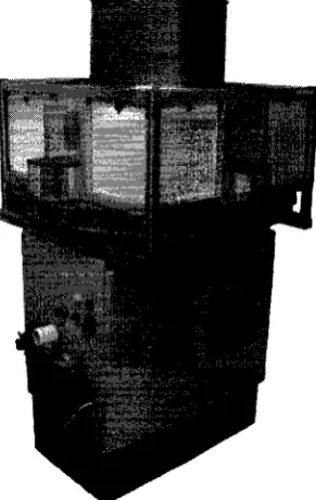
The Optisorter, seen in Fig. 2.1, was a German engineered MV system built in the early 1990s. A number of these systems were acquired by Pharmaphil Inc. to be implemented as an affordable quality control method for the manufacturing of their size # 0 0 - # 5 two part gelatin capsules. Although the Optisorter has a solid mechanical foundation for an MV system, the hardware was essentially obsolete. The exact functionality of the Optisorter is still unknown, however the hardware contained therein gives a good indication of what functions this system may have performed.
2. SYSTEM OVERVIEW
Figure 2.1: Optisorter External View
2.1.2 Summary of Operation
2. SYSTEM OVERVIEW
2.2 System Timing
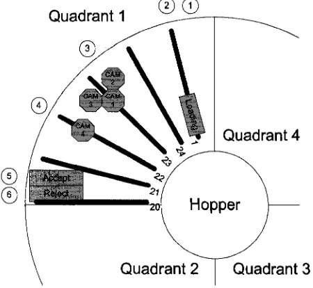
To understand the most important factors in system timing, let an event represent an operation that will be occurring in the system when an arm arrives at a certain location and a cycle represent the time it takes for a new arm to arrive at an event, in other words, the time between arms. Major events will include:
1. Clearing the holder. 2. Loading the holder.
3. Imaging the top of the capsule. 4. Imaging the bottom of the capsule.
5. Accepting the capsule. 6. Rejecting the capsule.
Fig. 2.2 shows the details of quadrant one with six of the 24 arms that will appear in the quadrant at a single cycle. The general location of the enumerated events above are show as circled numbers.
2. SYSTEM OVERVIEW
©0
Quadrant 3
Figure 2.2: Quadrant 1 Detailed
This was found by determining the number of capsule a single arm would have to inspect in this time and then computing how fast this arm would have to move in order to accomplish this task. Equation 2.1 shows this computation.
1000 caps I vain
10.4167 rev/min (2.1) (24 arms/rev x 4 caps/arm)
Since a cycle represents 1/24 of a revolution, the maximum time allocated to any event can be computed as shown equation 2.2.
60 sec/min
x (1/24) rev = 0.24 sec (2.2)
10.4167 rev/min
2. SYSTEM OVERVIEW
2.3 Imaging Environment
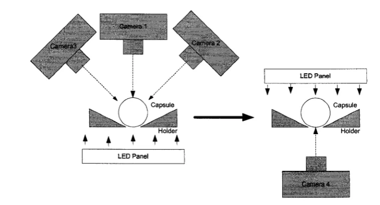
The current Optisorter system uses four cameras to capture the full 360 degree surface of the capsule. The capsule is seated in an opaque holder with a slot down the middle which allows both the top and back surfaces of the capsule to be visible. The capsules are illuminated with back lighting to cast the outline of the capsule and any defects in shadow while illuminating the background and flawless portions of the body for the capsule. Three cameras are positioned to examine the top surface of the capsule while a single camera is positioned from the reverse angle to examine the bottom of the capsule. The cameras are angled to image as much of the surface as possible, however, the solid metal holder occludes a small portion where the capsule makes contact with the holder. In an ideal imaging environment, the back lighting would remain perpendicular to the camera in order to reduce any uneven illumination that results from reflected light. It would appear that due to space constraints, a single panel of LEDs was used for back lighting the three top images while a separate panel of LEDs was used to back light the bottom of the image. Fig. 2.3 shows the details of the camera and lighting setup.
2.4 Objectives for Modification
As the project objectives state, the ultimate goal is to retrofit the existing Optisorter system with upgraded hardware to perform faster, more comprehensive inspections of the capsules. The following modifications were proposed as part of the final sys-tem upgrade. These modifications were to be developed as three separate parts by individual students.
2. SYSTEM OVERVIEW
. \
Camera3 / '
, ' - \
Camera 1
-\ \
\ \
^Camera 2
\
LED Panel
\yf
Camera 4
Figure 2.3: Camera Configuration
2. Develop a PC based computer vision system to perform image processing and analysis.
3. Develop new low cost digital cameras to acquire and transfer images.
The third modification listed above is the focus of this thesis where the first two items were developed my Neil Scott and Mohammad Islam respectively. More specific technical details regarding the requirements of these cameras will be discussed in subsequent section. For more information regarding the other project objectives, refer to thesis of Neil Scott and Mohammad Islam.
2.4.1 Selecting a Camera
2. SYSTEM OVERVIEW
1. Frame Grabber
The first possible approach would be to purchase very inexpensive image sensors that could be connected via a Frame Grabber card to a PC. This would result in extremely fast implementation, but the high cost of a frame grabber made this solution very undesirable, especially if the final system were to be mass produced.
2. Fire wire PC Interface
The second consideration was to create custom cameras with a high speed Firewire interface. Producing custom cameras would cost effective compared to the cost of a frame grabber. It would also allow the hardware to be rea-sonably upgraded. However the design of such cameras would require longer development time. This was still advantageous over the high cost of the frame grabber interface, however developing hardware and PC drivers for the Firewire interface would have been quite difficult due to the interface complexity and lack of commercial hardware and software support.
3. USB PC Interface
The final option was to continue with the idea of custom cameras, only with a slightly slower speed USB interface. The advantages of USB lay not only in the cost effectiveness, but in ease of development since many USB ready micro controllers and open sourced software were readily available. This was determined to be the optimal approach, as long as the USB transfer rates could keep up with required data throughput.
Since the most desirable d a t a interface was USB 2.0, a quick calculation was made
2. SYSTEM OVERVIEW
consist of 786432 bytes of data. USB 2.0 has a theoretical maximum transfer rate of 60 MB/s but this is unattainable due to packet communication overhead. Bulk transfer rates of up to 40 MB/s are possible with a realistic observable transfer rate of around 30 MB/s [3]. Preliminary USB 2.0 transfer test conducted by Neil Scott (a partner in this collaborative project) found a sustained bulk transfer rate of 31145280 bytes per sec or equivalently 30 MB/s. At this rate, it would take 0.1 seconds to transfer 4 full images to the PC. As 240 ms is the maximum cycle time available in order to achieve the desired system throughput, the USB interface would be sufficient and still leave up to 140 ms to be allocated for image processing to occur within the PC.
The preliminary system timing consideration outlined above showed that a USB 2.0 interface would be sufficient, and two demo boards were obtained to perform initial hardware feasibility tests.
2.4.2 Modifying the Imaging Environment
Although the current imaging setup may be sufficient, a number of improvements were proposed to provide improved images for processing. These included:
1. Improved lighting 2. Transparent holders 3. Three camera setup 4. Reflected front lighting 5. Reduced stray reflections
2. SYSTEM OVERVIEW
of using red LEDs, the diffused back lighting of the current system was upgraded to high intensity white LEDs. The higher intensity light allowed for a shorter exposure time while taking an image of the capsule, resulting in less blur introduced due to the movement of the capsule. The white light allowed for full color spectrum exposure of the color CMOS image sensors used in the final custom cameras.
The use of transparent holders for fixturing the capsules during imaging was tested, however, due to difficulties manufacturing perfectly clear holders free of scratches, the existing opaque holders were used. The use of clear holders should be considered as an area of future development.
A three camera setup was also tested, however without perfect clear holders, there are areas of the capsule that are occluded using three cameras and opaque holders. Again, the use of a three camera setup should be further investigate along with the use of clear holders.
The idea of reflected front lighting was proposed as a way of illuminating the front of an opaque capsule without needing an additional front light. The idea was to place a reflective surface over the front of the camera (around the lens) so that stray light from the back lighting of the capsule would be reflected and illuminate the surface of the capsule. This would provide the visibility required to identify color and surface defects. This item was tested and verified, however, was not implemented since the prototype was only desired to inspect clear capsules due to lack of project time.
2. SYSTEM OVERVIEW
2.5 Proposed Design
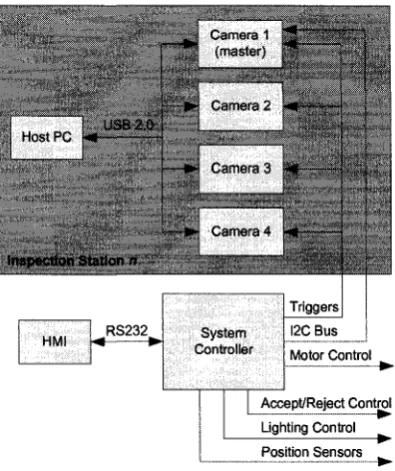
Using the understood operating principles of the existing mechanical system along with the desired areas of improvement, a basic proposed system overview was com-posed. This can be seen in Fig. 2.4.
Camera 1
i' ister) 1111-, •» ' . nera 2
* • ' . .iera3
»• v. .i oera 4
Inspection Station n g g
-HMI ># • RS232 System Controller
Ace
4 ( .
1
t
« • —
Triggers I2C Bus Motor Control
ept/Reject Control Lighting Control ___ Position Sensors
Figure 2.4: System Block Diagram
The design maintains the principal concept of having four identical stations work in parallel to accomplish the desired inspection throughput. These four inspection stations are connected via a custom control board that is responsible for co-ordinating the entire system. The control board acts as an interface between the mechanical systems and the computer vision stations, triggering the stations to capture an image of the capsules at the appropriate time and using the inspection results from the station to mechanically accept and reject the appropriate capsules.
2. SYSTEM OVERVIEW
send image data via a UBS 2.0 interface to a PC that is responsible for performing the necessary inspections. The results of the inspections are relayed through the master camera, back to the control board. Thus the proposed custom cameras must provide the following functionality:
1. Maintain the desired inspection rate.
2. Communicate image data to PC via USB 2.0. 3. Receive external triggers.
4. Output inspection results.
5. Remain competitive in cost compared to commercial systems. 6. Satisfy size constraints of existing imaging fixtures.
At this point, a proposed camera architecture was developed. Fig. 2.5 shows the most basic required functional blocks.
Imaging Sensor
Status and Timing
External Trigger Input
_ J _
Data Reconfigurable
Hardware Device
Inter-chip Communication Bus
Status and Timing Data
External Communication
Interface
USB 2.0 Communication
Interface
Memory Device
External USB Connection
External Communication I/O
Figure 2.5: Camera Block Diagram
2. SYSTEM OVERVIEW
image data and preparing the image data output. The image data is then be sent to a USB 2.0 capable microcontroller, which is responsible for the data communication to the PC for image processing. To satisfy the external communication requirements, an I2C bus extender was used along with simple 3.3 V inputs for receiving triggers.
A small EEPROM is also added to the design, in order to store basic configuration information such as the device identification for the USB enumeration as well as a master camera setting.
Chapter 3
Camera Design Methodology
3.1 Camera Design Flow
After identifying the objectives for the custom digital camera and how it was to operate as part of the larger system, a design procedure was developed. The major steps involved in the camera design methodology include:
3. CAMERA DESIGN METHODOLOGY
7. System integration
8. System testing
Fig. 3.1 shows the general bottom-up design flow for the proposed custom camera. With our camera specifications, performance requirements, desired operation and ba-sic overview in mind, this design procedure was developed to assist in the realization of the custom camera.
3. CAMERA DESIGN METHODOLOGY
3.2 Design Specifications
The system design specifications were based on inspection requirements outlined by Pharmaphil Inc. The details of both the business and defect detection requirements can be found in Appendix A. Table A.l outlines the inspection requirements used to derive the required resolution of the system. Table A.2 outlines the desired operation and is used to determine the required operating speed of the system as well as the test parameters. Finally, Table A.3 describes the desired features and functionality that must be incorporated into the modified design. Since the focus of this thesis is on the Camera Design with some insight into the imaging environment, Table 3.1 summarizes the pertinent specifications and the area of the system design to which they apply to.
Requirement
Defect size Capsule Colour
Speed of Inspection
Products Inspected
Specification
0.2mm or larger RGB/YUV
1000 caps/min
All
Applies to
Imaging sensor
Imaging Environment Imaging sensor
Imaging Environment Reconfigurable Hardware Imaging Sensor
Data Interface Memory/Buffering
Reconfigurable Hardware Table 3.1: Design Specification Summary
3.3 Major Design Methods
3. CAMERA DESIGN METHODOLOGY
design process.
3.3.1 Reconfigurable Hardware Programming
One of the largest portions of this design project involved developing hardware code for the reconfigurable device used on the camera. All coding was done in VHDL because of its modularity and easy readability (though Verilog coding would have been a viable substitute). The development environment used was Xilinx ISE 10.1 where the final VHDL code was synthesised.
The required VHDL coding was broken down into various behavioural blocks. Each block was behaviourally verified using an appropriate test bench when required, also coded in VHDL.
The top level VHDL block was assigned timing constraints with respect to the system clocks that would be provided to the system and final timing and resource utilization reports were generated. More specific information pertaining to the actual design results can be found in Chapter 6.
3.3.2 Simulation Tools
3. CAMERA DESIGN METHODOLOGY
6 and Appendix D.
3.3.3 Prototyping Hardware
Only limited hardware prototyping took place concerning the camera design. This was primarily due to the nature of the components, specifically their unique footprints that could not easily be mounted to a breadboard. Essentially, hardware prototyping took place by modifying demo boards. Ideally, multiple revisions of the final PCB would have been developed allowing for measurement of circuit noise and further adjustments. Details on the camera demo board used are outlined in the component selection section of the following chapter.
3.4 Testing
Chapter 4
Hardware Design
4.1 Component Selection
After the design specifications for the camera were determined, the next step was to select specific components capable of satisfying these requirements. Fig. 2.5 showed the major components that were to be included in the design. These include:
1. Imaging sensor
2. Reconfigurable device
3. USB 2.0 compatible microcontroller 4. External communication interface 5. Small memory device
4. HARDWARE DESIGN
4.1.1 Imaging Sensors
Two of the most heavily weighted factors in selecting hardware were: cost and avail-ability. Under these constraints, a variety of imaging sensors were compared for suitability. One critical decision was on whether to use a CMOS sensor or a CCD sensor as both have specific advantages and disadvantages.
Although they are faster and often cheaper than CMOS sensors, Charge Coupled Device (CCD) sensors only output an analog signal representing the charge result-ing from a pixel beresult-ing exposed to light. This analog value must be amplified and converted to a digital value by additional components and circuitry. On the other hand, a CMOS image sensor has an internal CCD with supporting digital circuitry integrated into the sensor itself. The sensor data output from a CMOS is in digital format and accompanied by associated timing signals for tracking the row and column of the current pixel being read out. In addition, CMOS sensors allow for windowing an area of the sensor's pixel array so that the entire image frame does not need to be outputted from the device. This provides greater control over both the exposure time of the sensor as well as the frame readout time. Micron, one of the primary suppliers of CMOS image sensors, provided a variety of demo boards with USB support. The sensors, though slightly more expensive than typical CCD sensors, were readily avail-able in large quantities and would not require as much additional hardware (i.e. a controller to integrate into the design) providing overall savings in development costs.
4. HARDWARE DESIGN
hardware selection in the first iteration of the design flow.
4.1.2 Reconfigurable Devices
The reconfigurable device on the camera plays a vital part in synchronizing the various hardware components as well as managing and processing image data. The reconfig-urable device acts as the camera's memory for all necessary image data buffering as well as a communication interface to the imaging sensor. Selecting a suitable device for such a dynamic role involved many considerations and making a number of trade offs. The decision parameters for selecting the appropriate device were as follows in order of priority.
1. Memory 2. Cost
3. Device Capacity 4. Development Time 5. Footprint
6. I/O Capacity
Initial firmware development was done on a Xilinx Virtex II series device (XC2V2500) as it was part of the Micron Demo board (MI3100 sensor head with DEM02 FPGA base) which was used as a basis for the final design. Since expandability of the ini-tial design was part of the camera design specifications, a reconfigurable device was required.
4. HARDWARE DESIGN
contain many tiny blocks of logic made up of flip-flops. CPLDs are "coarse-grain" devices with relatively few larger blocks of logic made up with flip-flops. FPGAs are RAM based and need to be configured each time they are powered up. CPLDs are EEPROM based and retain their memory after being programmed. CPLDs have faster input-to-output timing than FPGAs because FPGAs have a coarse-grain archi-tecture where a single logic block can implement a more complex function. However, FPGAs have special routing resources to implement efficiently binary counters and arithmetic functions (adders, comparators, etc.) and RAM, where CPLDs do not. In general, FPGAs can contain very large digital designs, while CPLDs can contain small designs only [11]. In order to satisfy the more sophisticated operations required by the reconfigurable device, an FPGA was selected as the more suitable device for this role.
Next, an appropriate FPGA was selected. As Xilinx ISE development software was readily licensed by the university with full access to support and CoreGEN designs, Xilinx FPGAs were favored over competing FPGAs such as Altera. This decision to use a Xilinx device was simply due to the availability of licensed development software as well as compatibility of code being developed on the demo board with a Xilinx FPGA.
4. HARDWARE DESIGN
Series
Spartan-3A DSP
Spartan-3AN
Spartan-3A
Spartan-3E
Spartan-3
Domain Description Cost (CAD)
DSP optimized For applications where in- $140 to $215 tegrated DSP MACs and
expanded memory are re-quired.
Non-Volatile For applications where non- $13 to $80 volatile, system integration,
security and large user flash are required.
I/O optimized Ideal for bridging, differ- $63 to $88 ential signaling and
mem-ory interfacing applications, requiring wide or multiple interfaces and modest pro-cessing.
Logic optimized Ideal for logic integration, $11 to $75 DSP co-processing and
em-bedded control, requiring significant processing and narrow or few interfaces.
I/O + Logic Opt. Ideal for highly-integrated $10 to $130 data-processing
applica-tions.
Table 4.1: Spartan FPGA Summary[19]
4. HARDWARE DESIGN
A final point on the FPGA selection relates to the powering of the device. Un-like the more expensive Virtex II devices, the Spartan series has some specific power requirements. In order to supply the correct voltages to the device with the proper power on start-up conditions, a separate component was chosen to perform this role. The TPS7500 Triple supply by Texas Instruments was chosen based on a recommen-dation in the device data sheet [21].
4.1.3 Communication Interface
There were two main components selected to act as communication interfaces for the camera. The primary device responsible for transferring image data to the PC is the Cypress CYCFX2. This specific device was selected by the developer of the USB 2.0 communication drivers so the details of this device are not covered in detail as part of this thesis.
One benefit of using this device is its ability to act as a data slave device. A 16bit data bus allows an external device to write data to a 4 KB FIFO within the Cypress controller that is automatically packeted and sent according to USB 2.0 communication specifications. The device also supports an I2C interface which is
utilized on the camera as part of the external communication interface. Finally, the device is relatively cheap which is an extremely important factor in component selection.
The second major device is the selection of an I2C bus extender. This allows the
local I2C bus on the camera to be connected to the control board for relaying the
4. HARDWARE DESIGN
4.1.4 Component Summary
Table 4.2 summarizes the major components selected for the device design noting how they will be referenced for the remainder of the thesis. For a complete list of components used in the device design, a bill of materials can be found in appendix C.
Device
Image Sensor FPGA
USB MCU Bus Extender Memory Triple Supply
Manufact urer
Micron Xilinx Cypress NXP Microchip
Texas Intruments
Part Number
MT9T001P12STC XC3S500E-4FTG256C CY7C68013A-100TAXC P82B715TD-T
24LC128-I/ST TPS75003RHLT
Referenced As
MT9T001 Spartan-3E FX2
I2C B E
128kB EEPROM TPS supply Table 4.2: Component Summary
4.2 Circuit Schematics
After having selected the specific devices to use in the camera design, the device connections must be carefully made to ensure their desired and correct operation. Some of the major considerations entail: powering the devices, terminating I/O, routing I/O and external connectors, sizing filtering capacitors, providing clocks, building reset circuits, designing power supplies and even placing test points on critical nets.
4.2.1 Micron MT9T001 CMOS Imaging Sensor
4. HARDWARE DESIGN
some particular considerations that had to be made when designing the schematics for this device as it required separate analog and digital power supplies. The purpose of these separate supplies is to isolate the very noisy digital circuitry from the analog portion of the IC, which is highly susceptible to noise in the power supply.
To improve the sensor's operation, separate analog and digital low drop-out linear regulators were used to power this device. However, the ground pins share the same grounding net. The appropriate placement of grounding points in the PCB layout of this device made this possible, reducing the effect any ground noise may have on the analog ground of the device by providing a direct path for the current to flow, preventing potential current leaks towards the other ground pins.
The power saving features of the chip have been grounded to simplify the PCB routing. The remaining data bus, timing signals and reset and status signals have been connected to pins on the FPGA for flexible control over this device. Fig. B.4 in Appendix B shows the final schematic drawing for the Micron MT9T001 sensor.
4.2.2 Xilinx Spartan-3E500 F P G A
4.2.2.1 I / O Connections
4. HARDWARE DESIGN
4.2.2.2 Clock Connections
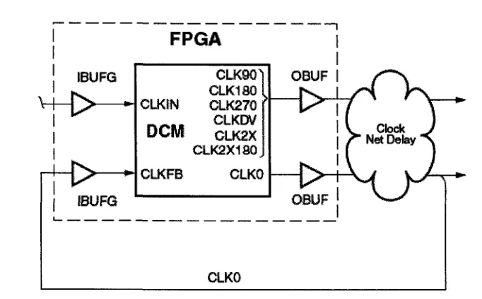
Special considerations were also made when connecting clock signals to the FPGA. Although the FPGA can internally route any I/O to any cell, the Spartan-3E de-vice has dedicated Digital Clock Managers (DCMs) with specific pins associated with them. Any part of the design where an output clock was supplied to another device, such as the clock for controlling exposure rate of the MT9T001 sensor, a neighbour-ing I/O pin was shorted to the DCM output in order to provide DLL feedback for the clock manager. The configuration of such a scenario can be seen in Fig. 4.1. For the specific case of the camera schematic net CLKIN (provided to the MT9T001 sensor from the FPGA),the net IFCLK enters the FPGA at IBUFG feeding CLKIN of the DCM (which is optionally shifted within the DCM). This is outputed from the FPGA at OBUF as the net CLKIN which is then connected to the MT9T001 sensor. The net CLKIN also re-enters the FPGA at the IBUFG feeding the CLKFB of the DCM to regulate the clock output. This configuration is essential to removing any clock skew that can occur through the FPGA device. This is critical, especially when the clock net is shared by multiple devices and routed through the FPGA. A similar configuration was used on the clock net (SCL) of the I2C communication bus.
4.2.2.3 Power Connections
4. HARDWARE DESIGN
FPGA
CLKIN
DCM
CLKFB
CLK901 CLK180 GLK270 CLKDV
CLK2X
CLK2X180,
CLKO
CLKQ
Figure 4.1: DCM with Off-Chip Delay Feedback
these capacitors is discussed in greater detail in a later section of this thesis.
4.2.3 T P S Triple Supply
The TPS7500 Triple Supply was selected as an ideal component to supply the FPGA with the required voltage levels for operation. This integrated circuit uses two non-synchronous buck converters to supply up to 3 A on the 3.3 V and 1.2 V lines. In addition, it has an integrated low-dropout linear regulator for the 2.5 V supply. Each supply has an adjustable "soft start" that allows the desired voltages to be increased at a controlled rate during power-on. This feature is used to satisfy the power on requirements of the Spartan-3E series FPGAs. The specifications for these voltages can be found in [21] and the voltage ramp rates are summarized in Table 4.3.
4. HARDWARE DESIGN
Symbol | Description Min Max Units
VCCINTR Ramp rate from GND to valid VCCINT supply 0.2 50 ms level.
VCCAUXR Ramp rate from GND to valid VCCAUX supply 0.2 50 ms level.
Vcco2i? Ramp rate from GND to valid Vcco supply 0.2 50 ms level.
Table 4.3: Spartan-3E Supply Voltage Ramp Rate[21]
components for the non-synchronous buck converters, selecting appropriate sized fil-tering capacitors and providing a reverse current path on the drain of the power transistors via Schottky diodes.
To suit the upgradable nature of the design, the supporting components were sized for a maximum current draw of 3 A. This is the maximum the TPS device can source. Even though the maximum current supplied from the USB controllers is limited to 500 mA, the cameras can handle external supplies capable of supplying greater currents for potential off-line application (such as additional testing and prototyping).
4.2.3.1 Limiting Buck Converter Current
The two non-synchronous buck converters that supply voltage to the VCCO and VC-CINT lines of the FPGA are both capable for sourcing up to 3 A (internally limited) unless externally limited by sizing Ri and i?2> as seen in Fig. B.l of Appendix B. Unlimited current allows the converters to operate in a continuous mode, preventing "ringing" from occurring in the junction of the PMOS transistors and inductors. For this reason, R\ and R^ were sized as to not limit current through these devices to any less than 3 A and at the same time, be capable of dissipating the maximum power. As power is a function of 72R with I at 3 A, R must be reduced as much as possible to
4. HARDWARE DESIGN
resistors were chosen for this application.
4.2.3.2 Setting VCCO
The non-synchronous buck converts are designed to sustain a 1.22 V output with a unity feedback. In order to set the voltage output of one of the buck converters greater than 1.22 V, the feedback to the converter must be appropriately scaled down (i.e., through a voltage divider circuit) so that the resulting output voltage is regulated at a desired level. Since the camera design operates on 3.3 V I/O, as specified in both the Cypress FX2 device as well as the MT9T001 image sensor, a single VCCO of 3.3 V was required and was generated using Buck2. The feedback output voltage for Buck2 can be written as:
VOUT = VFB (jl + l\ (4.1)
Since VFB = 1-22 V and VOUT — 3.3 V then RQ/RS = 1.705. Based on
recommen-dations from [15], i?6 and R5 were chosen as 61.9 kfl and 36.9 kfl respectively.
4.2.3.3 Sizing Soft Start Capacitors
4. HARDWARE DESIGN
4.2.4 Cypress FX2 USB Microcontroller
The schematics seen in B.3 for the Cypress FX2 microcontroller were essentially replicated from the Cypress CY3684/3674 EZ-USB Advanced Development Board. Slight modifications were made, such as connecting the reset pin directly to power through an RC circuit designed to delay the power on transient. As in the demo board, the analog power was shared with the digital power. The data bus pins for the slave FIFO were connected to the FPGA which was used to drive data to the device. The FX2 required an external clock. For this, a 24 MHz crystal was supplied. This clock was internally divided to produce a 48 MHz clock for IFCLK (used to synchronize the incoming FIFO data) as well as provide an external system clock CLKOUT. The CLKOUT net was supplied directly to the FPGA and was internally referenced as USBCLK, which can be scaled using a DCM of the FPGA and sent to the MT9T device to control exposure time.
The FX2 was also connected to the FPGA in a configuration that allowed it to program the FPGA in serial slave mode. With this setup, FPGA code could be loaded to the device through the USB port, eliminating the need for an additional program memory device or external programming connection. This also allowed the USB device drivers to supply the latest FPGA code whenever the device was plugged in, ensuring that the FPGA was always loaded with the most recent code. This also ensures that all cameras in a system will operate with the same code, without the need to update each FPGA of each camera separately.
4. HARDWARE DESIGN
4.2.5 I
2C Communication Bus
The I2C components were connected so that the data net (SDA) was shared between
all I2C devices, as was done with the clock net (SCL). Special considerations had to
be made to size the pull-up resistors on both the local side of the I2C bus as well as
the external side of the I2C bus extender.
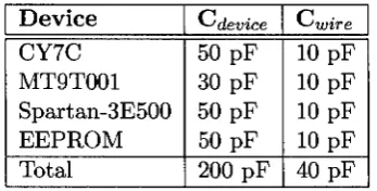
When calculating the pull-up resistance values, the gain of the signal buffers in-troduces scaling factors that must be applied to the system components. In practical systems, the pull-up resistance value is usually calculated to achieve the rise time requirement of the system [7]. For the purpose of this design, the I2C bus operated
at 100 kHz. Thus, the time constant of the total system (RC) is set to 1 us or less [12]. Equation 4.2 was used in determining the required pull-up resistance.
K>puU—
1/IS
up (4.2)
^device > ^wiring
On the local side of the I2C bus, the following components were connected with
their corresponding capacitive load on the bus and factored in as part of Cdevice- Table 4.4 shows these devices.
Device CY7C MT9T001 Spartan-3E500 EEPROM Total
^device
50 pF 30 pF 50 pF 50 PF 200 pF
{-'wire
10 pF 10 pF 10 pF 10 pF 40 pF
Table 4.4: I2C Devices: Loading Capacitance
The value of CWire was approximated as 10 pF for any copper traces to the device
4. HARDWARE DESIGN
this value was rounded down to the nearest common resistor value of 4 kf2.
On the external side of the I2C bus, the load capacitance was computed by
as-suming 50 pF per meter as outlined by [12]. For an approximate wire length of 2 m, a total capcitive load of 100 pF was used in Equation 4.2. The required pull-up resistance on the external side of the extender was found to be lOkO.
Also attached to the I2C bus was the small 128 kB EEPROM used to store device
settings such as master/slave settings, windowing parameters for the camera and device IDs for USB enumeration. Again, the SDA and SCL lines were connected to the bus and the device was powered appropriately. As can be seen in the schematics of B.5 of Appendix B, the I2C bus power is supplied by the same 3.3 V source as the
Cypress FX2 Microcontroller.
4.3 P C B Layout
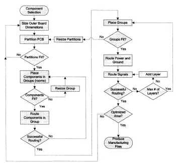
After having selected the desired components, a Printed Circuit Board was designed to create connections between the components, such as resistors, integrated circuits, and connectors [13]. In order to accomplish this task, the following bottom-up design approach was used (shown in Fig. 4.2).
4. HARDWARE DESIGN
Component \ Selection J
Size Outer Board Dimenstions
Partition PCB U | Resize Partitions k
.Yes Place Components in Groups (rooms)
.^Componentsv^ \ ^ Fit? /
: Y e s Route Components in
Group
Jr
/ Successfuf\ \ . Routing?/^
L
No
No
*
Resize Group 1
Yes
Place Groups
Yes
Route Power and Ground
f Produce X
( Manufacturing J V Files y
Figure 4.2: PCB Design Flow
4.3.1 P C B specifications
There were some restrictions on the physical characteristics of the PCB that had to be set before a layout could be designed. These included the following:
1. Maximum outer dimension <70 mm
2. Maximum of four layers on the PCB (two outer and two inner layers) 3. Space for four mounting through holes
4. HARDWARE DESIGN
foot of board. From this, the thickness of coper can be computed using the known density of copper. A typical copper weight used for low voltage electronics is 1 oz copper, resulting in a layer approximately 35 //m thick [6]. To verify that this would suit the camera PCB board, the following assumptions and calculations were made. First, because a FT256 footprint was used for the FPGA, a minimum trace width of 5mil was used (1 mil = 1/1000 inch). Second, the maximum current drawn through any of these traces to I/O in the FPGA was limited to 100 mA by the input clamp diodes [20]. Finally, the maximum temperature rise permitted for a trace was limited to 10 °C as was the minimum rise value in the IPC-2221 graphs used to determine thermal conductive properties of copper traces [6]. Using these values, the following required copper weight can be calculated.
Area[mils2} = (Current[Amps]/(k * Temprise[°C]b))1/c (4.3)
Width[mils] = Area[mils2]/(Thickness[oz\ * 1.378[mils/oz\) (4.4)
where for IPC-2221 internal copper layers: k=0.024, b=0.44 and c=0.725
From Equation 4.3 the required trace area for our design constraints can be de-termined as Area = 1.77 mil2. Using the area calculation and solving for Thickness
in Equation 4.4, the required copper thickness is 0.25 oz.
Thus 1 oz copper would be more than suffice for the requirements of the PCB design and will maintain the desired thermal performance during operation.
4. HARDWARE DESIGN
4.3.2 Component Placement
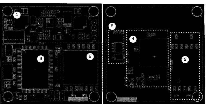
Component placement was the most critical step in the PCB layout, as this was the primary determining factor for successful routing of the design. The first step in component placement was to partition the PCB board in the major component groups. In total, there were 5 groups, one for each schematic drawing summarized above. These consisted of:
1. TPS Power Supply 2. Xilinx FPGA 3. Cypress FX2 USB
4. Micron MT9T001 image sensor 5. I2C components
Fig. 4.3 shows the final partitions and their layout on the PCB board. The top of the board is shown to the left with copper traces in red and the bottom of the board to the left with copper traces in blue. The shaded dotted rectangles outline the partition bounds and the white markings show component boundaries. However, before arriving to this final layout, a number of iterations were performed as outlined in Fig. 4.2.
4. HARDWARE DESIGN
Figure 4.3: PCB Partitions and Final Layout
of the board. Thus the remaining large components were placed on the top side (red). The two linear regulators used to power this device (U6, U7) were placed adjacent to each other in the ample free space surrounding the MT9T001 with the corresponding input and output capacitors placed near their corresponding pins. These were later routed through the power plane layer to MT9T001.
4. HARDWARE DESIGN With the TPS75003 fully routed in place, the placement of the FPGA (U2) and Cypress FX2 (U3) were both considered simultaneously. The FX2 was oriented such that the data pins for the 16 bit FIFO bus were facing closest to the FPGA. Both devices were also placed close the edge of the partition to facilitate successful rout-ing. The USB mini-B connector was placed within 100 mils of the device and trace lengths to the data lines were kept the same to prevent signal skew. Conveniently, the connectors were located at the edge of the PCB and appropriately spaced from any "tall" or high profile components which prevents possible obstruction from the mating connector. The 24 MHz crystal oscillator (Yl) was also placed near to its corresponding device pins to prevent signal degradation due to trace impedances. Power to the FX2 was routed through an internal power plane in the PCB, therefore, little consideration was paid to the placement of the 3.3 V linear regulator powering it. Finally, bypass, input and output capacitors were placed appropriately near their corresponding pins.
The FPGA (U2) was the simplest group to place as the only consideration nec-essary was the location of the 32 bypass capacitors required for the device. These were lined along the top and bottom of the device, spaced according to suggestions by [18], where very few signals were required to be routed. This left the main data buses for the MT9T001 image sensor and FX2 USB device free to be routed along the sides and center. Because there were many unused I/O on the FPGA, the device was placed at the edge of the PCB with very limited access to the pins along one side. The general signal breakout for buried pins (pins towards the center of the ball grid array) was planned according to the recommendations of [18].
The final group consisted of the I2C components. The bus extender was the most
critical component in this group to place because it needed to be as near as possible to the I2C connector on the PCB. This connector (JP3) was placed in the TPS75003
4. HARDWARE DESIGN
this device were made in the I2C partition on the bottom of the PCB. The I2C bus
extender chip (U8) was connected directly next to the connector, closely neighboured by the I2C EEPROM (U9).
4.3.3 Power and Grounding
Typically in a four layer design such as the camera PCB, the two internal layers are reserved for power and ground. This has two purposes: The first is to provide accessibility to power and ground pins on the surface layers, without obstructing routing; The second is to create a large capacitance between the power and ground planes, which are usually separated by a dielectric pre-preg. Since the thickness of the pre-preg is easily adjustable, the capacitance created between the two inner layers can be optimised better than the FR-4 material that composes the PCB layers themselves
[6].
The goal in routing the power plane layer is not only to provide surface components with accessibility to the appropriate voltages in this layer. It also to maximises the copper area, increasing the effective capacitance of the plane. In addition, minimizing bends or loops in the plane helps to reduce any parasitic inductances that could result
[18].
Fig. 4.4 shows the final power plane routing with six separate planes; one for each required voltage on the device. These voltages include: 3.3 V I2C and digital/analog
4. HARDWARE DESIGN
Figure 4.4: PCB Power Plane Layout
4.3.4 Bypass capacitors
The purpose of a bypass capacitor network is to filter digital switching noise, providing a smooth impedance profile over a range of frequencies, thus ensuring a static voltage level at the power pins of a device.
4. HARDWARE DESIGN
varying capacitor values throughout this range so that the total number of capacitors equals the total number of pins. However, since smaller capacitive values contribute less to the overall impedance profile [1], a greater number of these capacitors needs to be placed. In general, the number of capacitors should be doubled for every decade decrease in capacitance. Fig. 4.5 shows an example of a selection of capacitors for a 48 power pin device. Note that the quantity of capacitors increases as the capacitance decreases. Fig. 4.6 shows the impedance profile resulting from the capacitor selection of Fig. 4.5. This selection of capacitors results in a fairly even impedance over the range of 1MHz to 100 Mhz.
Quantity 2 7 13 26 Symbol • 1 • • Package E 0805 0603 0402 Capacitive Values (|iF) 680 2.2 022 0.022 Parasitic inductance (tiH) 2.8 2.0 1.8 1.S Parasitic Resistance (ohms) 0.57 0.02 0.06 0.20
Figure 4.5: Bypass Capacitor Values
t E . t »
1S01
e
I
i,emtmm
I.&0S 1.1
Pen* Values ol FfeiaM C« (stKSees [ohms]
\ > \
\
p'
/
—~yy
7
1.E«1 \.hM XSiM U t£*m
Figure 4.6: Bypass Capacitor Impedance Profile [1]
per-4. HARDWARE DESIGN
formance of the bypass network. This is because the routing to the bypass capacitor adds to the equivalent series inductance (ESL) of the device. Fig. 4.7 shows how an inductive loop can be formed in the cross-section view of the PCB, where current can travel through the power plane, up a via, across the capacitor, down a via and back through the ground plane. The size of this loop needs to be minimized to reduce the inductive effects contributing to the equivalent impedance of the capacitor. Due to this effect, the placement of a capacitor on the PCB can have a substantial effect on the effective resonant frequency of the capacitor. Fig. 4.8 shows the impedance profile of a capacitor and how the inductive and capacitive components influence the resonant frequency of the device. Basically, the capacitive component reduces the impedance, while the ESL of the device increases the impedance with respect to an increase in frequency. As the trace lengths between the power pin of a device and the bypass capacitor increases, the resonant frequency of the device shifts and may make the capacitor ineffective in filtering the desired noise from the system. Thus the bypass capacitors should be placed as close to the device power pins as possible, generally less than 100 mils away.
Another reason to keep to the bypass capacitors near the power pins of the device is to improve the response time of the capacitors to fluctuations in voltage. A small drop in charge at the device power pin takes time to propagate to the capacitor. The capacitor then releases charge which must then propagate back to the device. During this time, the voltage level could drop below the device's required operating range (if the distance to the capacitor is too large), indicating that the response time to these fluctuations is too slow.
4. HARDWARE DESIGN
0402 Capacitor Body
Surface Trace
Power and Ground pianes
Mounted Capacitor Current Loop
Figure 4.7: Capacitor Placement Inductive Loop[l]
Impedance
Total Impedance Characteristic
Inductive
Contribution (ESL)
Capacitive Contribution (C)
X623_04JJ72S02 Frequency
4. HARDWARE DESIGN
Figure 4.9: Bypass Capacitor Critical Current Path
routed in the power network where the estimated current path contributing to ESL is highlighted.
4.3.5 Routing
4. HARDWARE DESIGN
4.3.6 Manufacturing Files
The final step (after defining the PCB physical characteristics, placing components and routing connections between the components) was to generate the required files for manufacturing. These are listed below.
1. Board Stackup: defines the order of the four layers, board thickness and pre-preg.
2. Dill Holes: defines location and size of holes for the PCB such as mounting points and through hole component footprints.
3. Copper Etch: defines the areas of copper on the four layers that compose the routing of the design.
4. Solder Mask: defines areas of the board protected against solder. This en-compasses everything except where the component pins will be soldered to the copper board.
5. Solder Paste: defines areas where solder paste will be applied for mounting components.
6. Silk Screen: defines the coluored print and artwork on the PCB used to identify components and component locations.
7. Pick and Place: defines the location of the components to be placed relative to the pick position on the components package.
4. HARDWARE DESIGN
9. Assembly Drawing: defines specification for how to assemble mechanical com-ponents on the PCB if this is required. This was not included in the camera design.
Chapter 5
HDL Blocks and Programming
5.1 F P G A Programming Overview
The FPGA was used in the camera design to act as the main controller to the various components within the camera. These functions included:
1. Frame timing and data synchronization 2. Digital Clock Management (DCM) 3. I2C communication
4. Data buffering FIFO 5. Output control 6. Image processing
5. HDL BLOCKS AND PROGRAMMING
Image Sync Signals * • Image Data
I2C Bus
USB Data Out
USB Sync Out -xi
Clocks IN/OUT
AJL
DCMs
Frame Sync.
I2C Comm.
Output Control
Triggers IN/OUT
r
Trigger Timing/ Delay
System Regs.
Image Processor
Shift Control
-MM
5x5 WindowI
Image Construction
32K FIFO
Line Buffer [0:W-1] |
Line Buffer [0:W-1] |
Line Buffer [0:W-1] |
Line Buffer [0:W-1] I
Color Conversion
3
Figure 5.1: FPGA VHDL Modules and Data Flow
With these functions in mind, a block diagram was developed to show the data flow through the FPGAs various functional blocks. Fig. 5.1 shows the proposed ar-chitecture for the VHDL code developed for the FPGA in the camera design.
The following sections describe the development of these blocks and their VHDL realization.

![Table 4.1: Spartan FPGA Summary[19]](https://thumb-us.123doks.com/thumbv2/123dok_us/1468028.1179862/48.615.98.532.91.452/table-spartan-fpga-summary.webp)