Broadband Class-J/F
−1Continuum Mode Design Utilizing Harmonic
Efficiency Selectivity Circuit
Gideon Naah1, *, Songbai He1, Weimin Shi1, Bin Song1, Tian Qi1, and Shaddrack Y. Nusenu2
Abstract—This paper proposes a harmonic efficiency selectivity circuit (HESC) for achieving a broadband Class-J/F−1 continuum mode power amplifier (PA) with enhanced efficiency. Design
equations are derived through continuum mode condition analysis and are used in implementing the HESC. The implemented HESC topology is then used in attaining the broadband Class-J/F−1 continuum mode PA. A theoretical parameter termed harmonic-alpha (ρh) acting as a sub-unit structure in HESC is introduced. Considering harmonic losses,ρh possesses a lookup table containing information on the harmonics. ρh operates in unison with the HESC in selecting the suitable harmonics with the best efficiencies. With ρh, the relationship among the HESC, the optimal impedance at the device’s drain, and the terminal load impedance is defined for a greater freedom of harmonic impedance solutions space, efficiency improvement, and bandwidth extension, thus, indicating an increased flexibility in the design of broadband continuum mode PAs. This method is validated with a realized PA prototype operating from 1.3 to 2.4 GHz corresponding to a fractional bandwidth of 59.5%. The experimental results under continuous wave signals indicate that 79% peak efficiency, 42.68 dBm peak output power, and 16.96 dB peak gain are recorded. Moreover, at 1.7 GHz, when being tested with modulated signals at an average output power of 34.83 dBm, the lower and higher adjacent channel power ratios (ACPRs) without digital predistortion (DPD) are −34.9 dBc and −33.9 dBc, respectively, and a drain efficiency (DE) of 45% is recorded. With DPD, −50.8 dBc and−50.3 dBc are respectively obtained at lower and higher ACPRs at an average output power of 34.6 dBm, and a DE of 44% is achieved.
1. INTRODUCTION
High efficiency broadband PAs are sought after in current and next generation wireless communication systems compared to their single/narrow band counterparts. These wireless communication systems possess rigorous standards for communication. For this cause, PA researchers are actively devising new methods of designing PAs in meeting the stringent requirements for these wireless systems. A typical example of such type of PA is the Class-J continuum mode initially proposed by Cripps et al. in 2009 [1]. In succession, alternative methods have been utilized by other PA researchers in improving the performance of the classical continuum mode PAs based on Class-B/J, Class-J, Class-F, and Class-F−1
as published in [2–12].
The standard Class-J continuum mode PA has both resistive and reactive parts in its fundamental harmonic load impedance whereas its second harmonic load impedance has only a reactive part as presented by Cripps in [7]. In [8] for example, a resistive part was introduced in the second harmonic load impedance in a series of continuous modes PAs to further extend the impedance spaces. Similarly
Received 2 June 2018, Accepted 12 July 2018, Scheduled 7 August 2018 * Corresponding author: Gideon Naah ([email protected]).
in [10], continuous Class-F PA using the nonlinear embedding transfer function was introduced with the main goal of determining feasible load impedance design spaces and nipping the limitation of the second harmonic load impedance’s trajectory in the bud. As noted, the fundamental harmonic and the reactive second harmonic in Class-J do incur harmonic losses, deleteriously affecting its output power, efficiency [6], and of course its bandwidth.
In this paper, the introduction of ρh parameter with derived equations for the fundamental and second harmonic load impedances of continuum mode PAs is adopted in the design of the HESC topology. Through this method of analysis, an HESC structure is designed and then used in implementing and meeting the design target of the Class-J/F−1 continuum mode PA condition. These derived equations provide helpful information in the analysis and design of continuum mode PAs. With
ρh parameter, the reactive parts in both the fundamental and second harmonic load impedances can be
suitably tuned, leading to the acquisition of maximum performances.
Additionally, ρh possesses a sampled lookup table for the drain efficiency (ηJd) sensitivity analysis of the Class-J/F−1 continuum mode PA. The lookup table is generated based on equations derived for
ρh and ηJ
d parameters to help continuum mode PA designers in facilitating the design to fabrication
procedure and avoiding the dependency on circuit optimization process including post-fabrication tuning. The laborious voltage and current waveforms’ analysis carried out in continuum mode PA design [3, 8, 11] are avoided. The harmonic losses are also characterized.
The proposed design approach generates extensive harmonic impedance solutions space, efficiency improvement, and broadband design flexibility as will be shown hereafter. The proposed technique is verified with a designed, fabricated, and measured 1.3 to 2.4 GHz Class-J/F−1 continuum mode PA prototype. The effectiveness of the proposed architecture is fully validated by the measurement results, evidently showing its advantages over other recently reported continuum mode PAs. A comparison is made with some contemporary related works as outlined in Table 2.
2. ANALYSIS OF THE CLASS-J/F−1 CONTINUUM MODE
To commence with the analysis of the proposed approach in a simple manner, take a keen look at the illustration of the proposed HESC scheme depicted in Fig. 1. As schematically illustrated in the figure, signal source is the point through which the input signal is fed into the PA; ZS the source impedance
at the input matching network; CGH40010F device is the model of transistor employed; Ropt is the
optimal impedance at the device’s drain required by the HESC topology for suitable impedance match;
ρh defines the theoretical parameter termed harmonic-alpha which acts as a sub-unit structure in the
proposed HESC architecture; ZL is the terminal load impedance. The internal structure of the HESC
topology is the one enclosed in the black-dotted rectangular box shown on the extreme right which is mapped onto a simplified HESC on the left side. To device drain is the point of connection between the HESC topology and the CGH40010F device model. The HESC topology is an output matching network attached to the drain of the transistor model.
Firstly, a load-pull simulation is carried out, and an impedance is obtained. For example, the obtained impedance from load-pull simulation is 16 +j ∗16.5 Ω. From the viewpoint of Fig. 1, it is
Zs
ZL
ρ
hMirror image of ZL
Ropt
CGH40010F Device
Signal Source
To Device Drain
Ropt
HESC
very essential to study the relationship as well as the interactions among the HESC, Ropt, and ZL in
this analysis at the nth harmonic frequency which is denoted by nf0 in the design of broadband high efficiency continuum mode PAs. From this juncture, the real part of the obtained impedance which is 16 Ω is assigned to Ropt. Hence, the normalized ρh equation is then derived as:
ρh=
Ropt ZL
@nf0, n= 1,2,3, . . . (1)
Equation (1) indicates that the suitable harmonic load impedance capable of ensuring extensive design space, efficiency improvement, and broadband design flexibility at the device’s drain is acquired atRopt
and then matched toZL. This phenomenon occurs at a specified harmonic frequency level chosen by the
continuum mode PA designer as indicated by @nf0, n= 1,2,3, . . . in Equation (1). Based on this,Ropt
should be varied from 16 Ω to 50 Ω with a determined step-size for efficient analysis using Equation (1). It means that to obtain the corresponding value for ρh whenRopt= 15 Ω for example, ρh = 0.547. And
when Ropt = 16 Ω for example, ρh = 0.5657. So for whatever value of Ropt obtained, it must be fed
into Equation (1) and varied to the desired value ofZLusing the preferred step-size discretion forRopt
from the continuum mode PA designer. The main idea behind varying Ropt is that in the literature,
the performance of continuum mode PAs is usually worse than the theoretical results. This is due to the inability of the network not finding a suitable matching. In view of this limitation, the proposed method might be more suitable and practical in finding the appropriate design space where optimal matching is guaranteed.
Conventional continuous mode PAs evolves from the standard narrow band Class-B PA’s condition. For convenience, the equations pertaining to the current and voltage waveforms of the standard Class-B condition are respectively presented as follows:
ids(θ) = Imax·
1
π +
1
2cos(θ) + 2
3π cos(2θ)
(2)
υds(θ) = VDD·(1−αcos(θ) +βcos(3θ))·(1−γsin(θ))−1≤γ ≤1 (3)
whereImaxis the maximum current of the transistor in Equation (2). The drain current in Equation (2) is normalized toImax. VDD is the drain bias voltage in Equation (3). In Equation (3), the waveforms are
defined as Class-B to Class-J continuum whenα= 1 andβ = 0 [9]. In that sense, it isαparameter that determines the continuum mode condition. Therefore, this is the fundamental concept of continuum mode PAs.
In Equation (4) [11], i1 (fundamental current) and iDC (direct current) components of Class-F−1
PA are shown
i(ϑ) =iDC−i1cos(ϑ) +i3cos(3ϑ) (4)
whereiDC = 0.37,i1= 0.43, and i3 = 0.06.
From Equations (1), (2), (3), and (4), the load impedances can be derived as follows:
ZJ1/F−1 = Ropt
√ 2iDC
2
3√3 +αsin(β·γ)·ρ
h+j∗R
opt
√ 2i1 20
3√3 +βcos(α·γ)·ρ
h (5a)
ZJ2 = Roptsin(ρh+β)α−j∗Ropt
3π 8 cos(ρ
h−β−α)·γ (5b)
ZJ3 = ∞ ·α·ρh (5c)
whereα and ρh determine the continuum mode design space condition with 0≤β ≤0.4;γ determines the step-size; Ropt = 2VDD/Imax defines the optimal class-B’s loadline resistance. The reason behind
this approach is in order for the extensiveness of the continuum mode condition to be effective and in finding the suitable Ropt for the HESC structure to be designed. For the unification and realization
of Equation (5), ρh must be positive. In situations where the obtained Ropt is negative, an absolute
value should be applied to eliminate its negativity. By this method, ρh works hand in hand with the derived equations forZJ1/F−1 andZJ2, offering a greater freedom of broadband continuum mode design
flexibility.
With the introduction ofiDC = 0.37 andi1 = 0.43 in the derivedZJ1/F−1 of the Class-J continuum
a boundary condition has to be set in order to ensure that the right values forρh are generated. These values are to be used in conjunction with the values inα to determine the continuum mode condition in the proposed Class-J/F−1 continuum mode. Therefore, the reactance part in the impedance obtained,
which is j∗16.5 Ω, must be divided by the resistance part which is 16 Ω by applying |XR| formula.
|X|
R ≈1.03 is then obtained. Hence,
|X|
R ≈1.03 puts a boundary condition onα and ρ
h inZ
J1/F−1 and
ZJ2 operation. Both real and imaginary parts in Equations (5a) and (5b) are varied utilizingα andρh.
The constraints are:
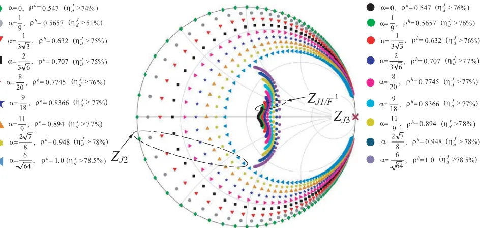
for α, 0≤α≤1 for ρh, 0.547≤ρh ≤ √2
3.8.
The effectiveness of these constraints are depicted in Fig. 3. ZJ2 beginning from the edge of the Smith
chart and extending much towardsZJ1/F−1 is an optimal approach. In other words, sweepingZJ2 from
the short circuit region and moving towardsZJ1/F−1, then to the open circuit region provides a greater
possibility of acquiring a suitable matching for the network under study. Otherwise, the performance of the HESC topology will be degraded due to much power consumption. The extensiveness ofZJ2 also
guarantees much wider design space, leading to the feasibilities of obtaining the HESC topology with optimal performance.
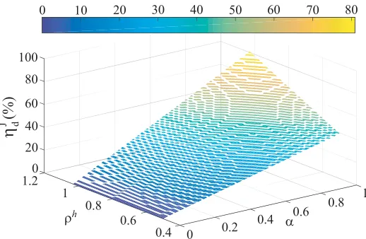
The derived drain efficiency equation represented byηJd for the proposed Class-J/F−1 continuum mode is expressed as:
ηJ
d =
π
4(α·ρ
h) (6)
where π4 is the standard Class-B’s efficiency, and α and ρh determine the continuum mode condition
where maximum efficiency is realized in the design space. Thus, when ZJ1/F−1 ∈ [α, ρh, nf0] =
[2√87,0.948,0.9], ηJ
d = 78.31% is obtained. In this case, the efficiency is quite lesser than the conventional
Class-B’s 78.5% drain efficiency by about 0.19%. However, with ZJ1/F−1 ∈ [α, ρh, nf0] = [√664,1,0.9], ηJ
d = 78.54% is obtained. This indicates 0.04% increment in the proposed Class-J/F−1 continuum
mode which is above that of the conventional Class-B’s 78.5% drain efficiency. Also, when ZJ2 ∈
[α, ρh, nf0] = [2√87,0.948,1.8], ηJd = 78.1% is achieved. In this scenario, the efficiency is still lesser than Class-B’s 78.5% drain efficiency by about 0.4%. However, with ZJ2 ∈ [α, ρh, nf0] = [√664,1,1.8], ηJ
d = 78.54% is also achieved. This indicates 0.04% increment in the Class-J/F−1 continuum mode
and is also above that of the conventional Class-B’s 78.5% drain efficiency. It can therefore be deduced that with α > √6
64 and ρ
h >1, extensive impedance solutions space, broadband capabilities, and drain
efficiency enhancement in the proposed Class-J/F−1 continuum mode are possible via the combination
0.4 1.2
1 0 20 100
40 60 80
0.6 0.8
0
0.6
1
0.2 0.4
0.8
0 10 20 30 40 50 60 70 80
h
η
J (% d
)
ρ α
Z
J2Z
J3 α= 0, ρ = 0.547 74%1
9, 0.5657 51% 1
3 3, 0.632 75% 2
3 6, 0.707 75% 8
20, 0.7745 7 6% 9
18, 0.8366 77% 11
9 , 0.894 7 7% 2 7
8 , 0.948 78% 6
64, 1 .0 78.5%
0, 0.547 76% 1
9, 0.5657 76% 1
3 3, 0.632 76% 2
3 6, 0.707 7 7% 8
20, 0.7745 77% 9
18, 0.8366 77% 11
9 , 0.894 7 8% 2 7
8 , 0.948 78% 6
64, 1 .0 78.5%
Z
J1/F-1α= α= α= α= α= α= α= α= (η h
ρ =h
ρ =h
ρ =h
ρ =h
ρ =h
ρ =h
ρ =h
ρ =h
dJ> )
(ηdJ> )
(ηdJ> )
(ηdJ> )
(ηdJ> )
(ηdJ> )
(ηdJ> )
(ηdJ> )
(ηdJ> )
ρ =h
ρ =h
ρ =h
ρ =h
ρ =h
ρ =h
ρ =h
ρ =h
ρ =h
α= α= α= α= α= α= α= α= α=
(ηdJ> )
(ηdJ> )
(ηdJ> )
(ηdJ> )
(ηdJ> )
(ηdJ> )
(ηdJ> )
(ηdJ> )
(ηdJ> )
Figure 3. Broadband harmonic impedance solutions space with>78% drain efficiency. The step-size is 0.1.
of Equations (5) and (6). Therefore, as long as the constraints on α and ρh are imposed, the proposed Class-J/F−1 continuum mode’s ηJd is beyond that of the standard Class-B and is sustained as shown in Fig. 2. A sampledρh lookup table containing information on the harmonics with their respective drain efficiencies is presented in Table 1.
Table 1. Sampled ρh lookup table for Class-J/F−1 continuum mode’s drain efficiency (ηdJ) sensitivity analysis obtained using derived ρh and ηJd equations.
α,ρh,ηJ
d(%) f0= 0.9 GHz 2f0= 1.8 GHz 3f0= 2.7 GHz 4f0= 3.6 GHz 5f0= 4.5 GHz
α= 0,ρh= 0.547,ηJ
d(%) 76.55% 74.6% 63.2% 66.67% 47.78%
α= 1
9,ρh= 0.5657,ηJd(%) 76.63% 51.63% 63.9% 67.22% 49.1%
α= 1
3√3,ρh= 0.632,ηJd(%) 76.92% 75.34% 66.1% 69% 53.6%
α= 2
3√6,ρh= 0.707,ηJd(%) 77.3% 76% 68.62% 70.9% 58.7%
α= 8
20,ρh= 0.7745,ηJd(%) 77.6% 76.6% 71% 72.63% 63.23
α= 9
18,ρh= 0.8366,ηJd(%) 77.82% 77.12% 73% 74.3% 67.5%
α=11
9,ρh= 0.894,ηdJ(%) 78.1% 77.62% 75% 75.8% 71.3%
α= 2√7
8 ,ρh= 0.948,ηJd(%) 78.31% 78.1% 76.8% 77.2% 75%
α=√6
64,ρh= 1,ηdJ(%) 78.54% 78.54% 78.54% 78.54% 78.54%
3. IMPLEMENTATION OF THE CLASS-J/F−1 CONTINUUM MODE
From the analysis, it is clearly observed that although both ZJ1/F−1 and ZJ2 yield drain efficiencies
higher than the standard Class-B mode, there is a marginal difference in their efficiencies at 2f0 when
α = 2√87 and ρh = 0.948 for example. At 2f0, ηdJ = 78.31% for ZJ1/F−1 whereas for ZJ2, ηJd = 78.1%.
Secondly, considering the CGH40010F device model, the sensitivities ofZJ2 and ZJ3 terminations
are reduced. This is due to the nonlinear device capacitance of the CGH40010F transistor for wave-shaping the voltage and current waveforms. Therefore, the design of the proposed scheme focuses more on ZJ1/F−1 matching. For PA realization, ifαh = √6
64 and ρ
h = 1, ηJ
d >78% is achieved. Therefore, αh = √6
64 and ρ
h = 1 are employed in the HESC design. Thus, extensive impedance solutions space,
broadband feasibilities, and enhanced efficiency for over 78% ηJ
d are at least rest assured. Utilizing
Equations (1), (5), and (6), the HESC topology can be designed and fine-tuned when necessary to achieve the proposed HESC architecture. Note that the same procedure could be used in designing the PA’s input matching network.
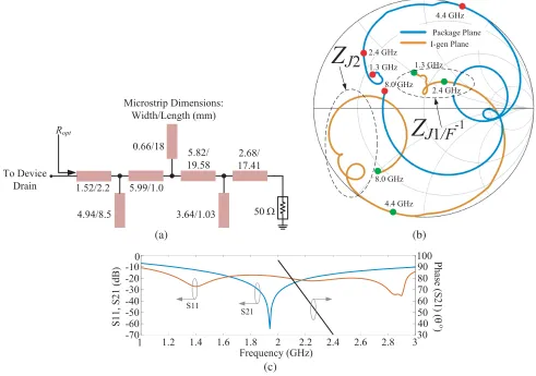
The proposed broadband HESC topology with microstrip dimensions is schematically illustrated in Fig. 4(a). The synthesized HESC topology’s impedance trajectories at package and current-generator (I-gen) planes achieved by de-embedding are plotted in Smith chart as evidently depicted in Fig. 4(b). At the I-gen plane, Ropt is normalized to 36 Ω at 1.3, 2.4, 4.4, and 8.0 GHz. It is shown that the
fundamental and second harmonic impedances in Fig. 4(b) are within the regions shown in Fig. 3. This supports the proof and feasibility of the proposed approach used in designing the broadband HESC topology. The S-parameters’ simulation results are shown in Fig. 4(c) including the optimal phase needed for the Class-J continuum mode operation. The phase provides a somewhat reduced overlap between the drain voltage and current waveforms. This phenomenon is a significant characteristic of the Class-J mode as presented in [9]. The needed phase, i.e., 45◦ in the proposed Class-J continuum mode
(a) To Device
Drain
50Ω
Ropt
Frequency (GHz)
1.2 1.4 1.6 1.8 2 2.2 2.4 2.6 2.8 3
Phase (S21) (
θ
)
1
S11, S21 (dB)
30 40 50 60 70 80 90 100 -10
0
-20 -30 -40 -50 -60 -70
S11
S21
1.52/2.2
4.94/8.5
5.99/1.0 0.66/18
5.82/ 19.58
3.64/1.03
2.68/ 17.41 Microstrip Dimensions:
Width/Length (mm)
(c)
1.3 GHz 2.4 GHz
4.4 GHz
8.0 GHz 1.3 GHz
2.4 GHz
4.4 GHz 8.0 GHz
Package Plane I-gen Plane
(b)
Z
J
2
Z
J
1
/F
-1ο
Figure 4. (a) HESC topology with microstrip dimensions, (b) impedance trajectories of HESC at package and I-gen planes in Smith chart (Roptis normalized to 36 Ohm), and (c)S-parameters simulation
occurred at 2.3 GHz, thus enabling significant possibilities in the realization of optimal bandwidth and efficiency performance.
3.1. Design Steps
(1) Perform a single step load-pull simulation instead of series of load-pull simulations.
(2) Assign the obtained load impedance toRoptand by using Equation (1), varyRoptwith a determined
step-size to a specified load impedance (ZL) and harmonic frequency level (nf0) based on the
discretion of the PA designer.
(3) Set boundary conditions for α and ρh based on the resistive (R) and reactive (X) parts of the acquired load impedance using |XR|.
(4) From step (3), feed in the acquired boundary conditions into Equation (5) and use Equation (6) in unison with Equations (1) and (5) to determine: (a) extensive impedance solutions space, (b) broadband feasibilities, and (c) enhanced efficiency. It is at this point that the suitable harmonic load impedance with the best properties meeting requirements (a)–(c) is selected.
(5) If conditions (a)–(c) in step 4 are not satisfied, repeat steps (3)–(4) until these conditions are satisfied.
(6) Use Equation (5) in designing the HESC structure for achieving the Class-J/F−1 continuum mode PA.
4. MEASUREMENT RESULTS
Based on the preceding theoretical design strategy presented in Sections 2 and 3, a broadband Class-J continuum mode PA with 1.3–2.4 GHz frequency of operation is designed employing Keysight Advanced Design System software and CGH40010F device model from Wolfspeed. The circuit is implemented on a Rogers RO4350B substrate with height, h = 30 mil, and relative permittivity, εr = 3.66. The
gate-voltage of the PA is biased at Vgs = −2.8 V and its drain-voltage at Vds = 28 V. The PA is fed with
29 dBm input power. The fabricated PA is graphically shown in Fig. 5(a).
The simulated and measured results are shown in Fig. 6. As evidently shown in Fig. 6, the simulated results achieve 52.73%–81.18% DE, 52.38%–79.26% power added efficiency (PAE), 40.84–42.69 dBm Pout, and 11.84–13.69 dB gain. The maximum DE (81.18%) occurred at 2.38 GHz. The fabricated PA was tested under continuous wave (CW) signal excitation, and the test results are depicted in Fig. 6. With the CW signal excitation, 53.6%–79% DE, 53.2%–77% PAE, 39.6–42.68 dBm Pout (which is equivalent to 9.12–18.54 W), and 12.6–16.96 dB gain are reported. The maximum recorded DE which is 79% in measurement occurred at 1.75 GHz.
(b)
0 0.2 0.4 0.6 1.4 1.6 -0.25
0.5
0 0.75 1 1.75 2 2.25
0 20 10 30 50 40 60 80 70 90 110 100 120
0.25 1.25 1.5
2.5 2.75
0.8 1 1.2
Time (psec)
Vds
(V)
I
ds
(A)
(a)
Frequency (GHz)
DE,PAE (%)
Pout (dBm)
Gain (dB)
1.4 1.6 1.8 2 2.2 2.4
10 1.3 60 70 80 90
30
20 40 50
Pout-Measured DE-Measured
Gain-Measured DE-Simulated
Pout-Simulated Gain-Simulated
PAE-Measured PAE-Simulated
Figure 6. Simulated and measured results of the fabricated broadband PA.
-50 -40 -30 -20 -10 0 20
10
1.64 1.66 1.68 1.7 1.72 1.74 1.76 Frequency (GHz)
Normalized PSD (dBm/Hz)
w/o DPD with DPD
Figure 7. Normalized power spectral density (PSD) with a 20-MHz LTE signal and 7.5 dB PAPR without and with DPD correction at 1.7 GHz.
Demonstrated in Fig. 7 is The measured broadband Class-J continuum mode PA’s linearity performance without and with the correction of DPD utilizing a 20-MHz bandwidth LTE signal with 7.5 dB peak to average power ratio (PAPR) at 1.7 GHz. The lower and higher ACPRs without DPD correction are −34.9/ −33.9 dBc respectively at an average output power of 34.83 dBm and with a recorded DE of 45%. With DPD correction, −50.8/−50.3 dBc were respectively obtained at lower and higher ACPRs, while the average output power was reduced to 34.6 dBm with a measured 44% DE. The performance of the proposed continuum mode PA still extends well below the design band although there is a discrepancy between measured and simulated results.
The origin of such discrepancy between measured and simulated results may be attributed to the follows by first observing Fig. 5(a) and Fig. 6: the HESC output matching network has much wider and longer transmission lines as shown in Fig. 5(a). As a result, it brings about losses in signal transmission, causing the 20% difference between theoretical and experimental DE and PAE at 2.1 GHz. This is clearly shown in Fig. 6. However, it is evidently shown in Fig. 6 that from 2.2 GHz and above, the DE and PAE begin to improve. This phenomenon is attributed to the lesser width possessed by the transmission line preceding the DC block capacitor. Also, fabrication errors contributed to losses in the measured PA.
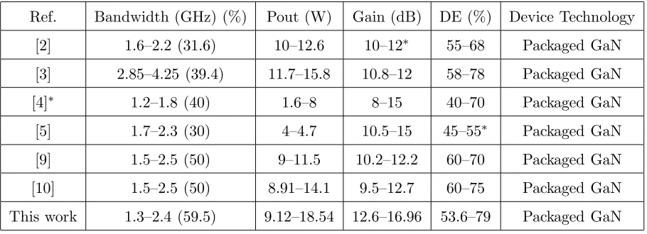
Table 2. Comparison with some recently reported broadband continuum mode PAs.
Ref. Bandwidth (GHz) (%) Pout (W) Gain (dB) DE (%) Device Technology
[2] 1.6–2.2 (31.6) 10–12.6 10–12∗ 55–68 Packaged GaN
[3] 2.85–4.25 (39.4) 11.7–15.8 10.8–12 58–78 Packaged GaN
[4]∗ 1.2–1.8 (40) 1.6–8 8–15 40–70 Packaged GaN
[5] 1.7–2.3 (30) 4–4.7 10.5–15 45–55∗ Packaged GaN
[9] 1.5–2.5 (50) 9–11.5 10.2–12.2 60–70 Packaged GaN
[10] 1.5–2.5 (50) 8.91–14.1 9.5–12.7 60–75 Packaged GaN
This work 1.3–2.4 (59.5) 9.12–18.54 12.6–16.96 53.6–79 Packaged GaN
∗: Read from graphs, Ref.: Reference, GaN: Gallium Nitride.
5. CONCLUSION
A design method for achieving broadband high efficiency Class-J/F−1 continuum mode power amplifier has been presented, demonstrating the feasibilities of extensive design space, broadband extension, and enhanced efficiency. Via the proposed approach, a harmonic efficiency selectivity circuit has been implemented and used in attaining the broadband high efficiency Class-J/F−1 continuum mode power amplifier. In measurement, 9.12 W–18.54 W output power, 12.6 dB–16.96 dB gain, and 53.6%–79% drain efficiency are recorded in the entire 1.3 to 2.4 GHz frequency band of operation. This band of operation corresponds to 59.5% fractional bandwidth. The experimental results have confirmed the validity of the proposed method and meeting the specified design frequency target. Thus, by the proposed method, competitive results are realized and are comparable to contemporary related works on continuum mode power amplifiers.
REFERENCES
1. Cripps, S. C., P. J. Tasker, A. L. Clarke, J. Lees, and J. Benedikt, “On the continuity of high efficiency modes in linear RF power amplifiers,” IEEE Microw. Wireless Compon. Lett., Vol. 19, No. 10, 665–667, Oct. 2009.
2. Mimis, K., K. A. Morris, S. Bensmida, and J. P. McGeehan, “Multichannel and wideband power amplifier design methodology for 4G communication systems based on hybrid class-J operation,” IEEE Trans. Microw. Theory Tech., Vol. 60, No. 8, 2562–2570, Aug. 2012.
3. Li, Q., S. He, W. Shi, Z. Dai and T. Qi, “Extend the class-B to class-J continuum mode by adding arbitrary harmonic voltage elements,”IEEE Microw. Wireless Compon. Lett., Vol. 26, No. 7, 522– 524, Jul. 2016.
4. Bukvi´c, B. and M. M. Ili´c, “Simple design of a class-J amplifier with predetermined efficiency,” IEEE Microw. Wireless Compon. Lett., Vol. 26, No. 9, 699–701, Sep. 2016.
5. Amirpour, R., R. Darraji, F. Ghannouchi, and R. Quay, “Enhancement of the broadband efficiency of a class-J power amplifier with varactor-based dynamic load modulation,”IEEE Microw. Wireless Compon. Lett., Vol. 27, No. 2, 180–182, Feb. 2017.
6. Dong, Y., L. Mao, and S. Xie, “Fully integrated class-J power amplifier in standard CMOS technology,” IEEE Microw. Wireless Compon. Lett., Vol. 27, No. 1, 64–66, Jan. 2017.
8. Shi, W., S. He, Q. Li, T. Qi, and Q. A. Liu, “Design of broadband power amplifiers based on resistive-reactive series of continuous modes,” IEEE Microw. Wireless Compon. Lett., Vol. 26, No. 7, 519–521, Jul. 2016.
9. Wright, P., J. Lees, J. Benedikt, P. J. Tasker, and S. C. Cripps, “A methodology for realizing high efficiency class-J in a linear broadband PA,”IEEE Trans. Microw. Theory Techn., Vol. 57, No. 12, 3196–3204, Dec. 2009.
10. Aggrawal, E., K. Rawat, and P. Roblin, “Investigating continuous class-F power amplifier using nonlinear embedding model,” IEEE Microw. Wireless Compon. Lett., Vol. 27, No. 6, 593–595, Jun. 2017.
11. Carrubba, V., et al., “Exploring the design space for broadband PAs using the novel continuous inverse class-F mode,”Proc. 41st Eur. Microw. Conf.(EuMC), 333–336, IEEE, Oct. 2011.