© 2015, IJCSMC All Rights Reserved 211 Available Online atwww.ijcsmc.com
International Journal of Computer Science and Mobile Computing
A Monthly Journal of Computer Science and Information Technology
ISSN 2320–088X
IJCSMC, Vol. 4, Issue. 1, January 2015, pg.211 – 221
RESEARCH ARTICLE
Comparative Study of 6T and 8T SRAM Using Tanner Tool
Rajnarayan Sharma
1, Ravi Antil
*2, Kamlesh Kumar
3¹M-Tech Department of ECE, MSIT, Sonepat, Haryana, India ²Assistant Professor, Department of ECE, MSIT, Sonepat, Haryana, India
³M-Tech Department of ECE,MSIT, Sonepat, Haryana, India
1
[email protected]; 2 [email protected]; 3 [email protected]
Abstract— In this paper we focus on the dynamic power dissipation during the Write operation in CMOS SRAM cell. The charging and discharging of bit lines consume more power during the Write ―1‖ and Write ―0‖ operation. 8T SRAM cell includes two more trail transistors in the pull down path for proper charging and discharging the bit lines.The results of 8T SRAM cell are taken on different frequencies at power supply of 1.5 V. The circuit is characterized by using the 130 nm technology which is having supply voltage of 1.5 V. Finally the results are compared with Conventional 6T SRAM cell. The power dissipated in low power 8T SRAM cell is reduced in comparison to conventional 6T SRAM cell. The result of the research has practical reference value for further study.
Keywords— SRAM, Tanner Tool, T-Spice, W-EDIT, IEEE
I. INTRODUCTION
SRAM is mainly used for the cache memory in Microprocessors, mainframe computers, engineering workstations and memory in hand held devices due to High speed and low power consumption. The need for low-power design is becoming a major issue in high-performance digital systems such as microprocessors [1], Digital Signal Processors (DSPs) and other applications. The increasing Market of mobile devices and battery powered portable electronic systems is creating demands for chips that consume the smallest possible amount of power. SRAM consist of almost 60% of Very Large Scale Integrated (VLSI) circuits. It is also said that memories are the biggest culprit for the power dissipation in any digital system and No digital system gets complete without memories.
© 2015, IJCSMC All Rights Reserved 212
like Half-Swing Pulse-Mode Techniques[5] these techniques are used for reduce the power dissipation of the SRAM circuit. All these discussed papers are used extra circuitry for reducing the power consumption.
In this paper optimized SRAM cell contains two extra tail transistors in the pull-down path of the respective inverter to avoid charging of the bit-lines. These two trail transistor are controlled by an extra signal write select (WS). During read or write mode at least one of the tail transistor must be turned OFF to disconnect the driving path of respective inverters.
II. RELATED WORK
Karimi and Alimoradi [6]: Rapid growth in semiconductor technology has led to shrinking of feature sizes of transistors using deep submicron (DSM) process. As MOS transistors enter deep submicron sizes, undesirable consequences regarding power consumption arise. This can be done by using one PMOS transistor and one NMOS transistor in series with the transistors of each logic block to create a virtual ground and a virtual power supply. Notice that in practice only one transistor is necessary, because of their lower on-resistance, NMOS transistors are usually used.
Cheng and Huang [7]: they present a low-power SRAM design with quiet-bit line architecture by incorporating two major techniques. Firstly, the authors use a one-side driving scheme for the write operation to prevent the excessive full-swing charging on the bit lines. Secondly, they use a precharge free pulling scheme for the read operation so as to keep all bit lines at low voltages at all times. SPICE simulation on a 2K-bit SRAM macro shows that such architecture can lead to a significant 84.4% power reduction over a self-designed baseline low-power SRAM macro.
Ming et. Al. [8]: They describes a low-power write scheme by adopting charge sharing technique. By reducing the bitlines voltage swing, the bitlines dynamic power is reduced. The memory cell's static noise margin (SNM) is discussed to prove it is a feasible scheme. Simulation results show compare to conventional SRAM, in write cycle this SRAM saves more than 20% dynamic power.
III. STATIC RAM
© 2015, IJCSMC All Rights Reserved 213
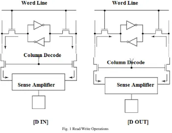
Fig. 1 Read/Write Operations
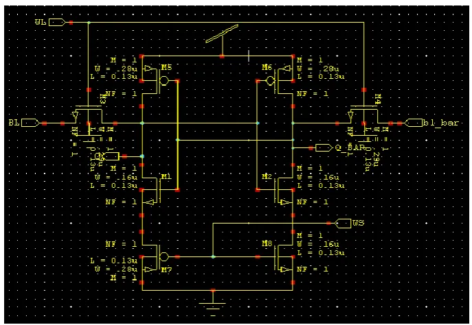
OPTIMIZED 8T SRAM CELL Schematic of 8T SRAM cell is shown in fig 2 In that we are using two more transistors M7 and M8 forreducing the power dissipation. WS signal is used forcontrolling the M7 and M8 during Write “0” and write “1”operation.
© 2015, IJCSMC All Rights Reserved 214
IV. COMPARISON ON DIFFERENT FREQUENCY
This section provides the detail simulation analysis of Low power SRAM cell for different frequencies. The dynamic power may be expressed as: P=αCV f.
A. SCHEMATIC DIAGRAM OF SRAMS (S-EDIT):
Fig. 3 Conventional 6T SRAM Cell (S-EDIT)
© 2015, IJCSMC All Rights Reserved 215
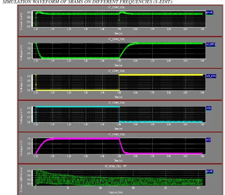
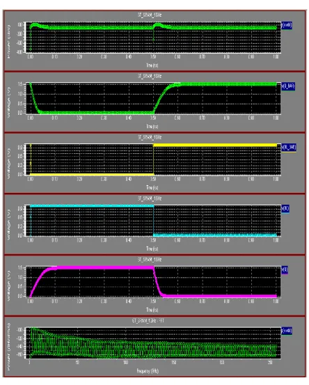
B. SIMULATION WAVEFORM OF SRAMS ON DIFFERENT FREQUENCIES (S-EDIT):
© 2015, IJCSMC All Rights Reserved 216
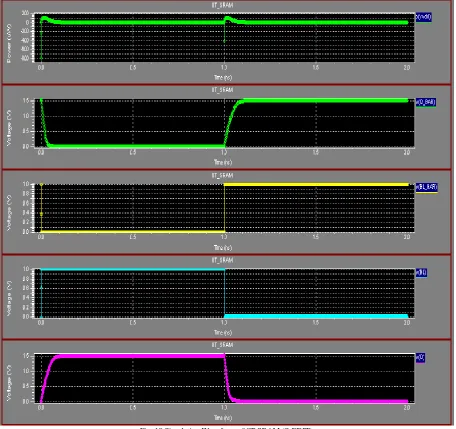
Fig. 6 Simulation Waveform of 8T SRAM at 1GHz (S-EDIT)
© 2015, IJCSMC All Rights Reserved 217
© 2015, IJCSMC All Rights Reserved 218
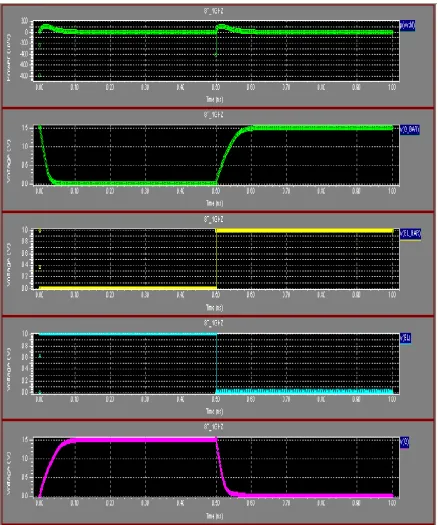
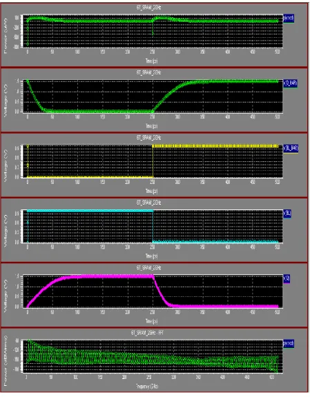
Fig. 8 Simulation Waveform of 8T SRAM at 2GHz (S-EDIT) TABLE I
COMPARISION ON BAISES OF FREQUENCY
Frequencies Power Dissipation in 6T SRAM cell (µw)
Power Dissipation in 8T SRAM cell (µw)
1 GHz 6.75 4.72
2 GHz 9.854 8.782
© 2015, IJCSMC All Rights Reserved 219
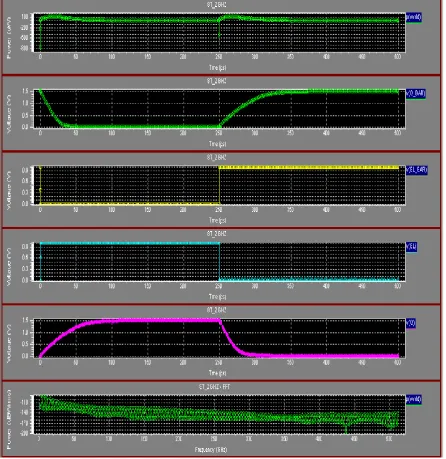
C. SIMULATION WAVEFORM OF AVERAGE POWER DISSIPATION AND DELAY (S-EDIT):
© 2015, IJCSMC All Rights Reserved 220
Fig. 10 Simulation Waveform of 8T SRAM (S-EDIT) TABLE II
COMPARISION TABLE
Different SRAM cells Average Power Dissipation Delay
6T SRAM 6.75 µw 5.44 ns
8T SRAM 5.52 µw 3.86 ns
© 2015, IJCSMC All Rights Reserved 221
V. CONCLUSION
Most of the developed low-power SRAM techniques are used to reduce only read power. Since, in the SRAM cell, the write power is generally larger than read power. We have proposed an SRAM cell to reduce the power in write operation by introducing two tail Transistors in the Pull-down path for reducing leakages. Due to this Stack Transistors the power dissipation has reduced from 18 % in comparison to Conventional 6T SRAM cell. The 8T SRAM provides power efficient solution. There is also improvement in the delay in case of 8T SRAM cell is 29% faster as compared to the conventional SRAM cell. So the newly designed low power SRAM cell consume lesser power and can be said that it is a power aware cell which is acceptable in today’s VLSI design market.
REFERENCES
[1] International Technology Roadmap for Semiconductors.[Online].Available: http://public.itrs.net.
[2] Mohammad Sharifkhani, Member, IEEE, and Manoj Sachdev, Senior Member, IEEESegmented Virtual Ground Architecture for Low-Power Embedded SRAM IEEE transaction on very large scale integration(VLSI) systems, vol. 15, no. 2, february 2007
[3] Mai, K.W., Mori, T., Amrutur, B.S., Ho, R., Wilburn, B., Horowitz, M.A., Fukushi, I., Izawa, T. and Mitarai, S. (1998), “Low power SRAM design using half-swing pulsemode techniques”, IEEE J. Solid-State Circuits, Vol. 33, pp. 1659-71.
[4] Vkita, M. et al. (1993), “A single-bit line cross-point cell activation (SCPA) architecture for ultra-low power SRAM’s”, IEEE J. Solid-State Circuits, Vol. 28, pp. 1114-8.
[5] Low-Power SRAM Design Using Half-Swing Pulse-Mode Techniques Kenneth W. Mai, Toshihiko Mori, Bharadwaj S. Amrutur, Ron Ho, Bennett Wilburn, Mark A. Horowitz, Isao Fukushi, Tetsuo Izawa, and Shin Mitarai IEEE journal of solid state circuits, vol. 33, no. 11, november 1998
[6] Gholamreza Karimi1 and Adel Alimoradi “Multi-Purpose Technique to Decrease Leakage Power in VLSI Circuits” Canadian Journal on Electrical and Electronics Engineering vol. 2, no. 3, March 2011.
[7] Shin-Pao Cheng and Shi-Yu Huang “A Low-Power SRAM Design Using Quiet-Bitline Architecture”Proceedings of the 2005 IEEE International Workshop on Memory Technology, Design, and Testing, 2005.