Two-Line Technique for Dielectric Material Characterization
with Application in 3D-Printing Filament Electrical
Parameters Extraction
Ali Al Takach1, 3, *, Franck M. Moukanda2, Fabien Ndagijimana1,
Mohammed Al-Husseini3, and Jalal Jomaah4
Abstract—The literature lacks detailed information about the electrical properties of the plastic filaments used in 3D printing. This opens the way for research on characterizing the types of materials used in these filaments. In this work, a method for the extraction of the dielectric constant and loss tangent of materials is described. This method, which is suitable for characterizing any dielectric material, is then used to characterize 3D-printed samples based on different filament materials and infill densities over a very wide frequency range [0.02–10 GHz]. The selected materials are Polylactic Acid (PLA), Acrylonitrile Butadiene Styrene (ABS) and a semi-flex filament that combines two important features of flexibility and endurance. These three types are the most commonly used in 3D printing. The two-line technique is applied to extract the complex permittivity of the material under test (MUT) from the propagation constant. This method employs the uncalibrated scattering parameters with different types of transmission line for any characteristic impedance. A rectangular coaxial transmission-line fixture has been used to validate the theoretical work through simulations and measurements involving the 3D filament samples.
1. INTRODUCTION
Nowadays, 3D-printing technology is frequently used in diverse applications (e.g., medical, manufacturing, telecommunication and electronics). The availability and low cost of this technology make it popular worldwide; furthermore, it is of great value when traditional fabrication tools fail in terms of complexity and/or cost. 3D printing is used in electromagnetic applications in different Radio Frequency (RF) and Microwave (MW) bands, for example in electromagnetic compatibility (EMC), low cost and lightweight TEM cells [1, 2]. Antennas [3], sensors [4], and metamaterial designs [5] are some other applications of 3D printing. This wide use of 3D printing in the electromagnetic field necessitates knowledge of the electrical properties of the dielectric materials used in printing, such as ABS, PLA, and Semi-Flex. The determination of the electromagnetic material properties, which are mainly composed of permittivity ε and permeability µ, is usually called material characterization. There are different techniques for material characterization, depending on the type of the material under test (MUT), its size, and the required accuracy of the extracted parameters. The material characterization methods are divided into two main categories: broadband and narrow-band [6]. Each method is based on the use of distributed and/or lumped elements. In this work, the non-resonant (broadband) technique and T -matrix conversion method are used. The latter is known for its accuracy and characteristic impedance independence. In this work, a method for the extraction of the dielectric constant and loss tangent
Received 17 July 2019, Accepted 10 September 2019, Scheduled 7 October 2019
* Corresponding author: Ali Al Takach ([email protected]).
of any dielectric material is described. As an application, this method is used to extract the complex permittivity of the plastic filaments used in 3D printing. The use of 3D printing is becoming more varied and widespread in RF and microwave circuits design. Thus, the knowledge of the electrical properties of the different types of 3D filaments and for different infill densities is essential for these and other applications. This detailed knowledge is not yet available in the literature, nor is provided by the sellers of 3D printing filaments.
2. MATERIAL CHARACTERIZATION
Material characterization determines electromagnetic properties versus frequency of the MUT by obtaining the permittivity ε and permeability µ, which describe the electromagnetic wave behavior within the material. In the material characterization method that we are describing, the complete step processes are sample preparation, fixture selection, measurement, and algorithm conversion.
2.1. Characterization Methods
We can divide material characterization methods into two main categories: resonant and non-resonant methods. The resonant method relies on the measurement of the resonant frequency and quality factor (ratio of resonant frequency to bandwidth) while the non-resonant method relies on the transmission/reflection measurement of the electromagnetic wave propagating within the structure [6]. The resonant method is applied by the resonator cavity with greatest accuracy, but only at discrete frequencies. The non-resonant method is used by the transmission line with less accuracy, but it provides extraction over a wide bandwidth. A comparison of the different material characterization methods is reported in [7]. The method choice and methodology depend on the level of accuracy needed, the desired simplicity of process and sample insertion, the chosen kind of test cell, and the bandwidth of interest. In this study, our interest concerns the extraction of the intrinsic properties of the 3D-printed plastic covering ultra-wide bandwidth, so we have selected the transmission reflection method.
2.2. Transmission Reflection Method
In the transmission/reflection method, the MUT is placed in a transmission line to disrupt the structure field lines and measure the material inherent properties [6]. Once the transmission line is defined, the use of the MUT in that fixture allows for measuring the S-parameters along with those of the reference in utilizing the vector network analyzer (VNA). The Two-line method used in this paper is an example of a Transmission Reflection Method.
2.3. Calibration Methods
Calibration denotes the removing of unwanted parts (e.g., cables or transmission-line adaptors) from measurements. This step is important for moving the reference plane of the measurement to the interface of the MUT. For the error that comes from the VNA and cables, the efficient calibration method used is the short, open, load and thru (SOLT) method [8]. This calibration method is popular: in most commercial VNA, there is a specific calibration kit that can contain all these standard loads to end the cables with them. Usually there is no problem with calibration of the coaxial cables that connect to the VNA. The critical problem starts when the error comes from the fixture itself, and there is then a need for a de-embedding method to remove this undesirable section (i.e., the MUT is usually centrally placed, and the connector areas should be removed). The SOLT method is not applicable here because there is no load available with these areas over the whole bandwidth. Therefore, the presented material characterization technique in this article has the advantage of extracting the electromagnetic properties without the need for the calibrated S parameters.
2.4. Conversion Techniques
Some of these techniques have limitations that resonate if the sample length is multiple of half wavelength. To overcome this limitation a branching problem should be solved. There are several suggestions in [13] to solve this ambiguity. In the subsequent paragraph, an advanced two-line technique is presented that has an advantage over the traditional method.
3. EXTRACTION METHOD
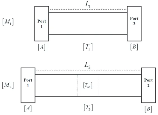
In some test fixture designs, the de-embedding of the connector-port adaptor transition is not possible due to the absence of standard matched loads. Another technique is needed to remove error effects from these areas. The presented two-line technique can solve this problem. The two-line technique refers to the multiline calibration method in [14–16]. This technique belongs to the group of Transmission/Reflection techniques for material characterization since it relies on measurement of the transmitted and the reflected propagating waves within the medium of interest. Implementation of the technique requires two transmission lines with the same physical and electrical properties but different lengths. IfL1 andL2, respectively, represent the lengths of the first and second lines, whereas ∆l=L2−L1 is the length difference between both lines, then the uncalibrated measuredS parameters in two scenarios with and without the MUT for the two lines are sufficient to accurately extract the propagation constant.
Figure 1. Test fixtures configuration.
Figure 1 exhibits the measurement configurations, and two transfer matrix forms can be employed: ABCD matrix and wave cascading matrix (WCM) [17]. In this work, we apply WCM because it gives the propagation constant parameter [18], and discontinuities are well-corrected. The WCM should be computed using Eq. (1).
[T] =
(
T11 T12
T21 T22
) =
−S11S22−S12S21
S21
S11
S21
−S22
S21 1 S21 (1)
S1 andS2 represent the uncalibrated scattering parameter matrices of the first and second test fixtures. These scattering parameters can be measured directly using a vector network analyzer (VNA).
[S1]⇒[M1], [S2]⇒[M2]
A and B are similar since we suppose that the two connector ports are mechanically and electrically identical [18]. In the cascading configuration, we can express the fixture as follows:
[M1] = [A] [T1] [B], [M2] = [A] [T2] [B] (2)
T1andT2 are the WCM of the first and second transmission lines. The multiplication of the long fixture by the inverse of the short fixture will result in the following:
[M12] = [M2] [M1]−1 (3)
[T12] ≡ [T∆l] = [T2] [T1]−1 (4)
[M12] ≡ [A] [T2] [A] [A]−1[T1]−1[A]−1 (5)
[M12] [A] = [A] [T12] (6)
T∆l is the WCM for the ∆l section. ∆l has the same characteristic impedance as the long and short
transmission lines but represents the ideal transmission line with no reflections. It is simply given as
[T∆l] = (
e−γ∆l 0 0 e−γ∆l
)
(7)
where γ is the propagation constant of the transmission line. The two WCM matrices M12 and T12 have the same eigen-values and related eigen-vectors [16]. As T∆l is a diagonal matrix, its eigen-values
are diagonal elements. The computation of the eigen-value of M12is shown as
[M12] =
(
m11 m12
m21 m22
)
(8)
eig([M12]) = (λ) (9)
whereas λis the eigen-value vector ofM12, which is calculated as follows:
( λ1
λ2
)
= (m11+m22)±
√
(m11−m22)2+ 4m12m21
2 (10)
Later, the average of the eigen-values is used as follows:
λ=eγ∆l (11)
From now, the MUT propagation constant is given by Eq. (13)
γ = lnλ
∆l (12)
Then, the phase constant β is the imaginary part of the propagation constant. Two main configurations are required in order to extract the MUT complex relative permittivity: with and without the sample under test (SUT).
βvac= Im (γvac), βM U T = Im (γM U T) (13)
Using Equation (15), we get the relative permittivity.
εr= (
βM U T βvac
)2
(14)
We here directly calculate the relative complex permittivity because the rectangle coaxial fixture is homogeneous. The dielectric loss tangent can be expressed [19] as
tanδ = 2
( αd βM U T −
αvac βvac
)
(15)
4. SIMULATION VALIDATION
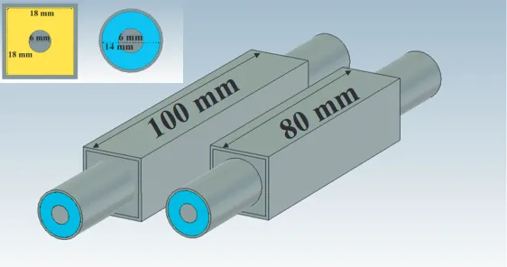
Validation of the extraction methodology was performed using a transmission line and two rectangular coaxial lines connected to 50 Ω connectors designed and simulated through the computer simulation technology (CST) microwave studio software. Two cases were simulated: with MUT as dielectric and without dielectric as a reference element. The fixture is filled with MUT.
Figure 2 is the design of the two fixtures and their lengths. To link the theoretical parameters to the simulated case, L1,L2, and ∆l are equal to 80 mm, 100 mm, and 20 mm, respectively.
Figure 2. Design of the simulated rectangular test fixture.
Figure 3 shows the extracted simulated permittivity of three different dielectric constants 2, 3, and 4, respectively. The extracted results establish the efficiency of the technique from uncalibrated
S-parameters over ultra-wideband.
Figure 3. Result of the extracted simulated permittivity.
Figure 4. Simulated dielectric loss comparison between software creation and two lines method extraction.
5. EXPERIMENTAL RESULTS 5.1. Coaxial Fixture Test
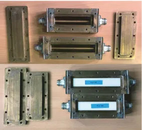
Rectangular coaxial transmission lines are used as a test fixture, as shown in Fig. 5, with two test space lengths 8 cm and 10 cm. The fixture is made with copper as a conductor and can be filled easily.
5.2. 3D-Printed Samples
The samples must completely fit the test space of the fixtures in order to avoid gaps, which affect the accuracy of the MUT-extracted property results. In the presented study, we selected the most commonly used material types in 3D printing, such as PLA, ABS, and Semi-Flex, to extract their intrinsic electric parameters: relative permittivity and dielectric loss tangent.
In addition to the electrical properties study, we studied the effects of the infill density percentage on the electrical properties. The infill density represents the percentage of plastic in the total volume of the 3D printed sample, and it is a parameter that can be controlled in the settings of the 3D printing software. The infill density is important because not all 3D printed samples are solely made of plastic. If the infill density is less than 100%, the sample is then made of both plastic and air. This fact helps researchers in the RF and Microwave applications to optimize their designs by using more accurate 3D-printing properties obtained by changing the infill density as needed. The prepared samples are shown in Fig. 6 for three types of plastic materials with three different infill densities: 100%, 50%, and 20%.
Figure 6. 3D-printed samples different materials and different infill density percentages.
The cross-section of the rectangle coaxial sample with the infill density percentage is shown in Fig. 7.
Figure 7. Cross section view of the rectangular sample with 100%, 50% and 20% of infill density percentages respectively.
5.3. Results
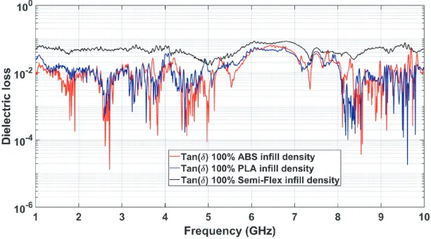
The dielectric constant versus frequency (2 MHz–10 GHz) of the three kinds of plastic samples with 100 % infill density is shown in Fig. 8. All of them are different from each other. PLA relative permittivity is lower than the ABS and Semi-Flex ones.
Figure 8. Permittivity of the ABS, PLA and Semi-Flex materials.
Figure 9 shows the dielectric constant when the infill density percentage changed in three cases (100%, 50%, and 20%) with the three MUTs (ABS, PLA, and Semi-Flex).
(a) (b)
(c)
The presented results for the dielectric constant show a relationship between the infill density percentage and the retrieved relative permittivity. An increasing infill density leads to a higher relative permittivity, and a smaller infill density results in a smaller relative permittivity. The relationship is not linear, but this opens the possibility for dielectric constant tuning by modifying the infill density percentage, and this will be very helpful in several RF and microwave applications.
To check the accuracy of the used Two-line method, it has been compared to the One-line method, as the results shown in Fig. 10. With the One-line method, only one of the two rectangular coaxial fixtures is used, where the MUT is placed inside. This method requires a short-open calibration to remove the effect of the transition between the N-type circular coaxial cable and the rectangular coaxial fixture. Later, the method in [20, 21] is used to obtain the propagation constant. Then, Equations (13)– (15) are used to compute the dielectric constant and loss tangent. The two methods, the Two-line and One-line, offer close results, but in addition to requiring calibration, the One-line method is less wideband than the Two-line method, as shown in Fig. 10.
Figure 10. Comparison of the used Two-line method with the One-line method for the ABS material.
On the other hand, Fig. 11 shows the loss tangent comparison for the plastic material (ABS, Semi-Flex, and PLA) with 100% of infill density. Fig. 12 exhibits the loss tangent comparison of the three plastic MUTs with three different values of infill density percentage.
In Fig. 12, some strange behavior in the variation of the loss tangent appears via higher loss tangent
(a) (b)
(c)
Figure 12. Dielectric loss tangent for ABS, PLA, and Semi-Flex plastic with three infill densities 100%, 50% and 20%.
at some frequencies with lower infill density. This response is also found in [22, 23] but is not explained. In our view, this phenomenon is due to the limitation of the extraction technique itself. It is known that in the transmission reflection material characterization technique, the permittivity extraction error percentage can be up to 5% while for the dielectric loss tangent, it is up to 10%. Also, Ref. [24] reports that the resolution of the extracted dielectric loss tangent is tan(δ) ≈ 0.01. Thus, the dielectric loss tangent cannot be extracted when the MUT has a low dielectric loss tan(δ)≪0.01. For tan(δ)>0.01, the 10% error percentage still exists, and it might lead to MUTs with smaller infill densities having a higher dielectric loss than MUTs with higher infill densities.
By looking at the extracted dielectric loss tangent responses, we note that for dielectric loss values less than 0.01, sharp drops in the dielectric loss value occur. This means that the extraction method is inaccurate for dielectric loss values less than 0.01. In the simulations, the extracted dielectric loss can be used when the value is>0.01 (also 0.01 for the measurements). This similarity between simulations and measurements proves that the conducting losses of the metallic material of the fixture have a critical effect on the limitation of the technique for the dielectric loss determination. As mentioned before, the non-resonant material characterization technique has acceptable accuracy over a wide bandwidth while the resonant technique has more accuracy at single frequencies. Therefore, for obtaining more accurate results of the dielectric loss tangent, the resonant material characterization technique should be employed for the dielectric loss behavior investigation at several frequencies.
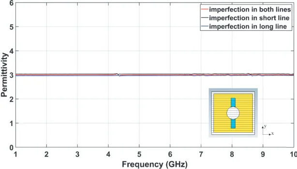
5.4. Imperfection Effect
We represent an imperfection by a rectangular cubic crack filled with air. Several simulations we ran indicated a crack in the middle of the MUT, around the inner conductor of the transmission line, which has a relatively more apparent effect on the extracted permittivity, because this is where the E-field lines are denser. Fig. 13 shows the extracted permittivity of a material with already known
εr = 3. A large imperfection is introduced in the center of the line where the effect is maximum. The
imperfection has the dimensions of 14×2×3 mm3. Three cases were considered: 1) the imperfection occurs in the sample placed in the short line; 2) the imperfection is in the sample placed in the long line; and 3) imperfections occur in both samples, although this has a lower probability of taking place. The results in Fig. 13 show that the extracted permittivity is resistant to the imperfections in the samples. The same conclusion is drawn when the imperfections occur away from the center of the lines, and in this case their effect is even more negligible.
Figure 13. Imperfection effect on extracted permittivity. The imperfection appears in blue around the inner conductor of the line.
6. CONCLUSION
In this work, the dielectric constant and loss tangent of the materials used in 3D-printing technology (ABS, PLA, and Semi-Flex) have been evaluated using an ultra-wideband characterization technique. We used the two-transmission-line technique to obtain their intrinsic electric parameters. Also, the infill density effects on the relative permittivity and the loss tangent have been studied by comparing three different percentages of infill density. The Two-line technique was described in details and validated through simulations and experimental measurements of ABS, PLA, and Semi-Flex material. This study focused on the use of the rectangular coaxial fixture as a test cell. No calibration of the measurement setup was required while using the described technique. The presence of the sample inside the cell disturbs the electromagnetic fields. Through mathematical formulas and using simulated and measured
S-parameters, the intrinsic electrical parameters of each dielectric sample are obtained.
ACKNOWLEDGMENT
This work is funded by the Beirut Research and Innovation Center (BRIC), in Beirut, Lebanon.
REFERENCES
1. Al Takach, A., F. Ndagijimana, J. Jomaah, and M. Al-Husseini, “3D-printed low-cost and lightweight TEM cell,” IEEE International Conference on High Performance Computing &
2. Al Takach, A., F. Ndagijimana, J. Jomaah, and M. Al-Husseini, “Position optimization for probe calibration enhancement inside the TEM cell,” IEEE International Multidisciplinary Conference on Engineering Technology (IMCET), 1–5, 2018.
3. Bongard, F., et al., “3D-printed Ka-band waveguide array antenna for mobile SATCOM applications,”IEEE 11th European Conference on Antennas and Propagation (EUCAP), 579–583, 2017.
4. Farooqui, M. F. and A. Shamim, “3D inkjet printed disposable environmental monitoring wireless sensor node,” IEEE MTT-S International Microwave Symposium (IMS), 1379–1382, 2017.
5. Kronberger, R. and P. Soboll, “New 3D printed microwave metamaterial absorbers with conductive printing materials,”IEEE 46th European Microwave Conference (EuMC), 596–599, 2016.
6. Chen, L. F., C. K. Ong, C. P. Neo, V. V. Varadan, and V. K. Varadan, Microwave Electronics: Measurement and Materials Characterization, John Wiley & Sons., 2004.
7. Shwaykani, H., A. El-Hajj, J. Costantine, F. A. Asadallah, and M. Al-Husseini, “Dielectric spectroscopy for planar materials using guided and unguided electromagnetic waves,”IEEE Middle
East and North Africa Communications Conference (MENACOMM), 1–5, 2018.
8. Padmanabhan, S., P. Kirby, J. Daniel, and L. Dunleavy, “Accurate broadband on-wafer SOLT calibrations with complex load and thru models,” IEEE 61st ARFTG Conference Digest, 5–10, 2003.
9. Vicente, A. N., G. M. Dip, and C. Junqueira, “The step by step development of NRW method,”
SBMO/IEEE MTT-S International Microwave and Optoelectronics Conference (IMOC), 738–742,
2011.
10. Rothwell, E. J., J. L. Frasch, S. M. Ellison, P. Chahal, and R. O. Ouedraogo, “Analysis of the Nicolson-Ross-Weir method for characterizing the electromagnetic properties of engineered materials,” Progress In Electromagnetics Research, Vol. 157, 31–47, 2016.
11. Kuek, C. Y.,Measurement of Dielectric Material Properties, Rohde & Schwarz, 2012.
12. Chen, X., T. M. Grzegorczyk, B. I. Wu, J. Pacheco, Jr., and, J. A. Kong, “Robust method to retrieve the constitutive effective parameters of metamaterials,”Physical Review E, Vol. 70, No. 1, 016608, 2004.
13. Arslanagi´c, S., T. V. Hansen, N. A. Mortensen, A. H. Gregersen, O. Sigmund, R. W. Ziolkowski, and O. Breinbjerg, “A review of the scattering-parameter extraction method with clarification of ambiguity issues in relation to metamaterial homogenization,” IEEE Antennas and Propagation Magazine, Vol. 55, No. 2, 91–106, 2013.
14. Eul, H. J. and B. Schiek, “A generalized theory and new calibration procedures for network analyzer self-calibration,”IEEE Transactions on Microwave Theory and Techniques, Vol. 39, 724–731, 1991. 15. Marks, R. B., “A multiline method of network analyzer calibration,” IEEE Transactions on
Microwave Theory and Techniques, Vol. 39, No. 7, 1205–1215, 1991.
16. Hasar, U. C., G. Buldu, M. Bute, J. J. Barroso, T. Karacali, and M. Ertugrul, “Determination of constitutive parameters of homogeneous metamaterial slabs by a novel calibration-independent method,”AIP Advances, Vol. 4, No. 10, 107116, 2014.
17. Frickey, D. A., “Conversions between S,Z,Y, H,ABCD, and T parameters which are valid for complex source and load impedances,”IEEE Transactions on Microwave Theory and Techniques, Vol. 42, 205–211, 1994.
18. Huynen, I., C. Steukers, and F. Duhamel, “A wideband line-line dielectrometric method for liquids, soils, and planar substrates,” IEEE Transactions on Instrumentation and Measurement, Vol. 50, No. 5, 1343–1348, 2001.
19. Pozar, D. M., Microwave Engineering, Wiley, 2005.
21. Zhou, L., S. Sun, H. Jiang, and J. Hu, “Electrical-thermal characterizations of SIW with numerical SOC technique,” IEEE International Conference on Computational Electromagnetics (ICCEM), 1–2, 2018.
22. Le, T., B. Song, Q. Liu, R. A. Bahr, S. Moscato, C. P. Wong, and M. M. Tentzeris, “A novel strain sensor based on 3D printing technology and 3D antenna design,”IEEE 65th Electronic Components and Technology Conference (ECTC), 981–986, 2015.
23. Mirzaee, M. and S. Noghanian, “High frequency characterisation of wood-fill PLA for antenna additive manufacturing application,”Electronics Letters, Vol. 52, No. 20, 1656–1658, 2016. 24. Krupka, J., “Frequency domain complex permittivity measurements at microwave frequencies,”