Miniaturized Dual-Band Antenna with a Rectangular Patch and
Symmetrically Placed Circles in the Partial Ground Plane
Baudha Sudeep*, Aman K. Goswami, and Manish V. Yadav
Abstract—This paper presents a miniaturized dual-band antenna with a rectangular patch and symmetrically placed circles in the partial ground plane. The dimensions of the proposed antenna are 15∗20∗1.5 mm3, and the antenna is excited by a 50 Ω microstrip line from the bottom. The proposed antenna is fabricated on the commercially available low-cost FR4 substrate having relative permittivity εr = 4.3 and loss tangent 0.025. By introduction of a rectangular slot with a T-shape in the ground plane and a rectangular patch, the lower frequency band is achieved. The peak gain and radiation efficiency of the proposed antenna are 2 dB and 78%. The proposed antenna operates at 2.846 GHz to 3.24 GHz and 4.05 GHz to 6.22 GHz frequency range. The antenna finds its application in S-band, 5.5/5.8 GHz WiMAX bands, and 4.9/5/5.9 GHz Wi-Fi bands.
1. INTRODUCTION
In this fast-paced world of wireless communication, miniature microstrip patch antennas find several applications due to their various advantages over conventional antennas. Its major advantages include compact size, light weight, radiation efficiency, low cost, ease of fabrication, and omnidirectional radiation pattern. In [1], a horizontal gap enhances bandwidth both at lower and higher frequencies. Antennas with planar shapes such as circle [2], ellipse [3], and triangle [4] were reported for wide bandwidth. For achieving dual broadband characteristic, a parasitic patch and slot are added in the ground plane [5]. Due to parasitic patch and slot better impedance matching occurs at the second operating band without affecting the performance of the first operating band. Bandwidth has been enhanced by 26% due to the introduction of a curved slot in the rectangular patch [6]. By adding a parasitic patch and rotating the slot, bandwidth has been enhanced drastically [7–9]. In [10], due to truncation of the corners and cutting symmetric circular slots in the radiating patch, bandwidth is enhanced in the higher frequency range. In [11], ultra-wideband (UWB) characteristics of a slot antenna have been observed by the introduction of a pair of parasitic patches. The combination of a U-shaped slot and rectangular parasitic patches is incorporated for the generation of higher-order resonance [12]. Making a parasitic patch and cutting a curved slot in the patch result in large impedance bandwidth, respectively [13, 14]. By achieving UWB characteristics, fractal geometry and rose leaf structure have been proposed [15, 16]. Bandwidth enhancement is reported due to adding a small fractal element in a microstrip antenna [17].
Lower frequency resonance is enhanced, and a better bandwidth is reported with a smaller size of the antenna than a rectangular slotted patch by the patch extensions introduced in the antenna design [18, 19]. UWB characteristics have been reported by introduction of a simple rectangular slot in the ground plane [20]. Recently a broadband characteristic has been reported due to compact planar antenna with stair-shaped ground plane [21]. By introduction of a U-shaped slit in the partial ground plane and rectangular parasitic patches adjacent to the microstrip line, UWB applications have
Received 22 November 2018, Accepted 3 January 2019, Scheduled 16 January 2019
* Corresponding author: Baudha Sudeep (sudeepb@goa.bits-pilani.ac.in).
been reported due to excitation of higher order resonance [22]. By variation of an E-shaped patch in a microstrip antenna, broadside radiation pattern has been suggested [23]. Stable omnidirectional radiation pattern over the entire UWB frequency has been reported by using rubber as a substrate [24]. A comparison between recently published monopole antennas is shown in Table 2.
In this paper, a miniaturized dual-band antenna with a rectangular patch and symmetrically placed circles in the partial ground plane is proposed. The lower frequency band is achieved due to introduction of a rectangular slot and T-shape in the ground plane. The proposed antenna operates at 2.846 GHz to 3.24 GHz and 4.05 GHz to 6.22 GHz frequency range (Magnitude of S11 <−10 dB). Various results of the proposed antenna will be discussed in the later sections.
2. ANTENNA DESIGN
The geometrical configuration of the proposed antenna is shown in Figure 1. The proposed antenna has a dimension of 15∗20∗1.5 mm3. The proposed antenna is fabricated on a commercially available low-cost FR4 substrate with relative permittivity εr = 4.3 and loss tangent 0.025. The antenna is fed by a 3 mm wide and 50 Ω microstrip line. The values of various parameters of the proposed antenna are shown in Table 1. The top portion of the proposed antenna consists of a rectangular patch of dimension (e∗a) and an extended microstrip line of total length of ‘b’, and ‘n’ is a height of the substrate. One side of the proposed antenna consists of a rectangular slot and two symmetrically placed circles with a T-shape attached to the partial ground plane, and the other side of the antenna consists of a rectangular patch with an extended microstrip line. CST microwave studio simulation software, a finite integration technique-based commercial electromagnetic simulator, is used to carry out computer simulation of the proposed antenna. Bandwidth enhancement is achieved due to the introduction of the rectangular slot,
(a) (b) (c)
Figure 1. The proposed antenna configuration, (a) top view, (b) bottom view and (c) side view.
Table 1. Parameter values of different sections of the proposed antenna.
Parameters Values (mm) Parameters Values (mm)
a 15 b 20
c 6 d 3
e 4 f 6
g 7 h 8
i 2 j 14.75
k 4.25 l 15.75
Table 2. A comparison between previously published monopole antennas.
Ref. Substrate Size (mm3) −10 dB S11BW (GHz) Antenna type
[1] FR4 38×38×1.6 3.62 to 7.32 Monopole
[22] FR4 35×25×1.5 2.9 to 16.3 Monopole
[2] FR4 52×62×1.5 2.4 to 11 Monopole
[3] FR4 42×42×1.5 3.45 to 13.22 Monopole
[4] FR4 46.5×57.6×1.5 3 to 5.8 Monopole
[5] FR4 25×25×1.5 2.4 to 6.1 and 9.4 to 13.8 Monopole
[6] FR4 50×55×1.6 2 to 6.8 Monopole
[7] FR4 31.5×31.5×1.6 3.4 to 5.6 Monopole
[8] FR4 51.5×61×1.5 1.8 to 6.9 Monopole
[9] FR4 45×45×1.6 2.23 to 5.35 Monopole
[11] FR4 37×37×1.5 2.1 to 11.1 Monopole
[12] FR4 35×25×1.5 2.9 to 16.3 Monopole
[15] RO3210 24×24×1.28 3.65 to 10 Monopole
[16] FR4 30×30×1.5 3.3 to 3.6 and 5 to 6 Monopole
[17] FR4 25×25×1.5 3 to 8 Monopole
[18] FR4 21×28×1.6 5 to 6 and 7.7 to 8.5 Monopole
[19] FR4 28×29×1.6 3.8 to 12 Monopole
[21] FR4 20×25×1.5 3 to 15.1 Monopole
[22] FR4 35×25×1.5 2.9 to 16.1 Monopole
Presented FR4 15×20×1.5 2.8 to 3.2 and 4.05 to 6.22 Monopole
two symmetrically placed circles and a T-shape attached in the partial ground plane. The miniaturized dual-band proposed antenna has been designed in three stages. Stage-01 is a simple antenna. One side of the antenna consists of a rectangular patch with microstrip line and partial ground plane in the other side of the antenna.
In the next stage (Stage-02), the microstrip line is extended in the patch so as to make its length ‘b’. A rectangular slot and two circles of radius ‘m’ are symmetrically placed on the ground plane. The final stage of the proposed antenna (Stage-03) is obtained by the same patch and attaching a T-shape to the partial ground, and all the stages are simulated using CST microwave Studio.
3. PARAMETER STUDY
In this section, various parameters of the proposed miniaturized dual-band antenna are discussed. Figure 2 shows the simulated return loss (magnitude of S11 (dB)) comparison of all three stages of the proposed antenna. Stage-01 is a simple antenna. The resonance is excited by a rectangular patch, and the finite ground plane shows an impedance bandwidth of 51% (5.3–8.9 GHz). By adding two parasitic circles with rectangular slot in the partial ground and extended microstrip line in the patch, the resonance is shifted to lower order band and shows a impedance bandwidth of 35% (4.8–6.8 GHz). Introduction of a T-shape in the partial ground plane results in dual bands as shown in Stage-03 (which is the final proposed antenna), and its impedance bandwidth is 13% (2.8–3.2 GHz) for the first band and 43% (4–6.2 GHz) for the second band.
Figure 2. Simulated return loss curve (magnitude ofS11 (dB)) in three stage.
Figure 3. Simulated return loss (magnitude of
S11 (dB)). Comparison of the proposed antenna with different parameter values of ‘e’ (all other parameters are fixed and have same values as in Table 1).
Figure 4. Simulated return loss (magnitude of
S11 (dB)). Comparison of the proposed antenna with different parameter values of ‘m’ (all other parameters are fixed and have same values as in Table 1).
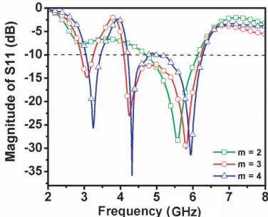
Figure 4 shows the comparison of simulated return losses (magnitude ofS11 (dB)) of the proposed antenna with different parameter values of ‘m’ where ‘m’ is the radius of the adjacent circle in the partial ground plane and demonstrates the variation of simulated return loss against operated frequency by varying the radius of ‘m’ in the bottom plane. As can be depicted from the return loss graph of Figure 4, for the optimum value of ‘m = 3 mm’, the frequency band shifts to lower frequency ranges, and the bandwidth tends to be maximum.
Figure 5 shows the simulated return loss comparison curves for different values of ‘k’ which is the height of the lower vertical strip in the ground plane. It is observed from the parameter study that as the value of ‘k’ changes, the resonance frequency changes; as the value of ‘k’ reaches 10 mm, the vertical strip of the bottom plane starts resonating in the lower frequency band and reaches up to 2.8 GHz, and (2.8–3.2 GHz) frequency band is obtained.
Figure 5. Simulated return loss (magnitude of
S11 (dB)). Comparison of the proposed antenna with different parameter values of ‘k’ (all other parameters are fixed and have same values as in Table 1).
Figure 6. Simulated return loss (magnitude of
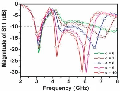
S11 (dB)). Comparison of the proposed antenna with different parameter values of ‘c’ (all other parameters are fixed and have same values as in Table 1).
4. SIMULATED AND MEASURED RESULTS
The fabrication of the proposed dual-band antenna has been done using (Phenix) Chemical etching method in the laboratory. Agilent Vector Network Analyzer (VNA), a 50 Ω SMA connector connected to the microstrip line and an anechoic chamber have been used for testing the proposed antenna.
Figure 7 shows the simulated and measured return loss curves (magnitude of S11 (dB)). It is observed from the return loss curves that the measured result is in good agreement with the simulated one, and it validates the simulated result. The measured result shows that the dual-band and its impedance bandwidth are 13% (2.8–3.2 GHz) and 43% (4–6.2 GHz).
Figure 8 shows the simulated and measured input impedance curves of the proposed antenna. The real part of the input impedance curve illustrates that the input impedance is maintained at 50 Ω throughout the operating frequency range. The imaginary part of the input impedance shows that the behaviour of the proposed antenna is inductive for most of the operating frequency range whereas for some frequencies it is capacitive, and it is observed from the curve that the measured results are in good agreement with the simulated ones.
(a) (b)
Figure 8. Simulated and measured input impedance (Real and imaginary parts) of the proposed antenna.
Figure 9. Simulated gain and radiation efficiency curves of the proposed antenna.
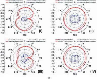
Figure 9 shows the simulated and measured gain/radiation efficiency curves with respect to the frequency of the proposed dual-band antenna. It is observed from the curves that the simulated and measured results are in good arrangement, and maximum value of the gain of the proposed antenna is 2 dB, and that of radiation efficiency is 78%. It is observed from the curves that both the gain and radiation efficiency attain their peak values in the operating frequency region of the proposed antenna. Figures 10(a) and (b) show the measured and simulated radiation patterns of the proposed dual-band structure with details of co-polarization and cross-polarization at four selected operating
(b)
Figure 10. (a)Simulated and measured Co-pol. and Cross-pol. of the proposed antenna at (I) 3 GHz
E-plane, (II) 3 GHz H-plane, (III) 4.22 GHz E-plane and (IV) 4.22 GHz H-plane. (b) Simulated and measured Co-pol. and Cross-pol. of the proposed antenna at (I) 4.94 GHz E-plane, (II) 4.94 GHz
H-plane, (III) 5.81 GHzE-plane and (IV) 5.81 GHzH-plane.
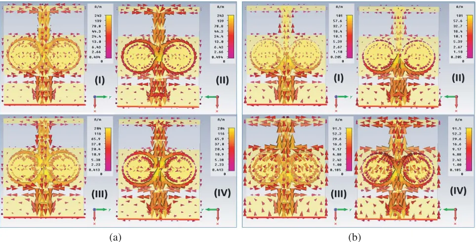
frequencies. The radiation pattern shows the direction in which an antenna radiates at a particular frequency. The H plane is shown on x-z plane (phi = 0◦) and the E plane shown on y-z plane (phi = 90◦). The stable omnidirectional and bi-directional co-polarization is observed with a good agreement with cross-polarization at the lower order frequency modes as shown in Figure 10(a) at (I) 3 GHz E-plane, (II) 3 GHz H-plane, (III) 4.22 GHz E-plane, and (IV) 4.22 GHz H-plane. The quasi-stable bi-directional and quasi-stable omnidirectional co-polarization is observed with an appropriate cross-polarization at higher order frequency modes as shown in Figure 10(b) at (I) 4.94 GHz E-plane, (II) 4.94 GHzH-plane, (III) 5.81 GHzE-plane, and (IV) 5.81 GHzH-plane. The behaviours of the radiation patterns of the proposed modified antenna in E-plane and H-plane satisfy monopole characteristics. Figures 11(a) and (b) show the surface current distribution of the proposed dual-band antenna at constant phase (212◦) for various selected operating frequencies at (I) 3 GHz (II) 4.22 GHz (III) 4.94 GHz, and (IV) 5.81 GHz. The current concentration at the upper edge of the adjacent circle (back view) with microstrip line (front view) as visible in Figure 11(a) as well as T-shape (back view) with rectangular patch (front view) is easily visible in Figure 11(b).
The current concentration is higher at the upper edge of the adjacent circle (partial ground plane) with microstrip line easily visible in Figure 11(a) at (3 and 4.22 GHz) frequencies, and the peak value of the surface current is 243 and 204 A/m.
(a) (b)
Figure 11. (a) Surface current distribution of the proposed antenna at selected frequency band of 3 GHz, (I) front view, (II) back view and 4.22 GHz, (III) front view and (IV) back view. (b) Surface current distribution of the proposed antenna at selected frequency band of 4.94 GHz, (I) front view, (II) back view and 5.81 GHz, (III) front view and (IV) back view.
5. CONCLUSION
A miniaturized dual-band antenna with a rectangular patch and symmetrically placed circles in the partial ground plane is proposed in this paper. The proposed dual-band antenna has an overall size of 15∗20∗1.5 mm3, and the proposed structure is fabricated and measured. Introduction of a rectangular slot with a T-shape in the ground plane has enhanced the bandwidth in the lower frequency band. The proposed antenna resonates in 2.846 to 3.24 GHz and 4.05 to 6.22 GHz frequency ranges and thus exhibits dual band characteristics with fractional bandwidth of 13% (2.8–3.2 GHz) and 43% (4–6.2 GHz). The real part is normalized to 50 Ω at the operating frequency band, and the behaviour of the antenna is inductive for the most of the operating frequency range whereas for some frequencies it has capacitive behaviour. The radiation efficiency and gain are in good agreement. The peak gain and radiation efficiency of the proposed structure are 2 dB and 78%, respectively. The stable radiation patterns with co-polarization and cross-polarization are observed (H-plane having an omnidirectional radiation pattern andE-plane having a bi-directional radiation pattern) over the entire dual-operating band which satisfy monopole characteristics of the proposed antenna. The surface current distribution shows good signal strength over the selected frequencies. Owing to all these properties, the proposed dual-band antenna is suitable for S-band, 5.5/5.8 GHz WiMAX bands and 4.9/5/5.9 GHz Wi-Fi bands.
REFERENCES
1. Wang, Y. J., C. K. Lee, and W. J. Koh, “Single-patch and single-layer square microstrip antenna with 67.5% bandwidth,”IEEE Microw. Antennas Propag., Vol. 148, 418–422, 2001.
3. Li, P., J. Liang, and X. Chen, “Study of printed elliptical/circular slot antennas for ultrawideband applications,” IEEE Trans. Antennas Propag., Vol. 54, No. 6, 1670–1675, Jun. 2006.
4. Chen, W. S. and F. M. Hsieh, “A broadband design for a printed isosceles triangular slot antenna for wireless communications,”Microw. J., Vol. 48, No. 7, 98–112, Jul. 2007.
5. Baudha, S. and D. K. Vishwakarma, “Miniaturized dual broadband printed slot antenna with parasitic slot and patch,” Microw. Opt. Technol. Lett., Vol. 56, No. 10, 2260–2265, 2014.
6. Baudha, S. and D. K. Vishwakarma, “Bandwidth enhancement of a planar monopole microstrip patch antenna,” Int. J. Microw. Wireless Technol., Vol. 12, 1–6, 2014.
7. Jan, J. Y. and J. W. Su, “Bandwidth enhancement of a printed wide-slot antenna with a rotated slot,” IEEE Trans. Antennas Propag., Vol. 53, No. 6, 2111–2114, 2005.
8. Jan, J. Y. and L. C. Wang, “Printed wideband rhombus slot antenna with a pair of parasitic strips for multiband applications,”IEEE Trans. Antennas Propag., Vol. 57, No. 4, 1267–1270, 2009. 9. Sung, Y., “Bandwidth enhancement of a microstrip line-fed printed wide-slot antenna with a
parasitic centre patch,” IEEE Trans. Antennas Propag., Vol. 60, No. 4, 1712–1716, 2012.
10. Baudha, S. and D. K. Vishwakarma, “Corner truncated broadband patch antenna with circular slots,”Microw. Opt. Technol. Lett., Vol. 57, 845–849, 2015.
11. Fan, S. T., Y. Z. Yen, B. Lee, W. Hu, and X. Yang, “Bandwidth enhancement of a printed slot antenna with a pair of parasitic patches,” IEEE Antennas Wireless Propag. Lett., Vol. 11, 1230– 1233, 2012.
12. Baudha, S. and D. K. Vishwakarma, “A compact broadband printed monopole antenna with U-shaped slit rectangular parasitic patches,” International Journal of Microwave and Wireless Technol., Vol. 8, 1231–1235, 2015.
13. Hasch, J., E. Topak, et al., “Millimetre-wave technology for automotive radar sensors in the 77 GHz frequency band,” IEEE Transactions on Microwave Theory and Techniques, Vol. 60, No. 3, 845– 860, 2012.
14. Ozturk, E., M. H. Nemati, et al., “SiGe process integrated full360 micro electromechanical systems based active phase shifter for W-band automotive radar,” IET Microwaves, Antennas and Propagation, 835–841, 2014.
15. Naqvi, S. A., “Miniaturized triple band and ultra-wideband (UWB) fractal antennas for UWB applications,” Microw. Opt. Technol. Lett., Vol. 59, 1542–1546, 2017.
16. Shan, K., C. L. Ruan, and L. Peng, “Design of a novel planar ultrawideband antenna with 3.5 and 5.5 GHz dual band notched characteristics,” Microw. Opt. Technol. Lett., Vol. 53, 370–375, 2011. 17. Fallahi, H. and Z. Atlasbaf, “Bandwidth enhancement of a CPW-fed monopole antenna with small
fractal elements,” AEU — Int. J. Electron. Commun., Vol. 69, 590–595, 2015.
18. Liu, C. Y., T. Jiang, and Y. S. Li, “A compact wide slot antenna with dual band-notch characteristic for ultra-wideband applications,” Journal of Microwaves, Optoelectronics and Electromagnetic Applications, Vol. 10, No. 1, 55–64, 2011.
19. Ali, J. K., M. T. Yassen, M. R. Hussan, and M. F. Hasan, “A new compact ultra wideband printed monopole antenna with reduced ground plane and band notch characterization,” PIERS Proceedings, 1531–1536, Kuala Lumpur, Malaysia, Mar. 27–30, 2012.
20. Kasi, B., L. C. Ping, and C. K. Chakrabarty, “A compact microstrip antenna for ultra wideband applications,” European Journal of Scientific Research, Vol. 67, No. 1, 45–51, 2011.
21. Sudeep, B. and K. V. Dinesh, “A compact broadband printed circular slot antenna with stair shaped ground plane,” Progress In Electromagnetics Research Letters, Vol. 74, 9–16, 2018.
22. Baudha, S. and D. K. Vishwakarma, “A compact broadband printed monopole antenna with U-shaped slit and rectangular parasitic patches for multiple applications,” International Journal of Microwave and Wireless Technologies, Vol. 8, 1231–1235, 2016.
23. Deshmukh, A. A., D. Singh, and P. Zaveri, “Broadband slot cut rectangular microstrip antenna,”
Science Direct, Procedia Computer Science, Vol. 93, 53–59, 2016.
24. Lakshmanan, R. and S. K. Sukumaran, “Flexible ultra wide band antenna for WBAN applications,”