N A N O E X P R E S S
Open Access
Strain analysis for the prediction of the
preferential nucleation sites of stacked quantum
dots by combination of FEM and APT
Jesús Hernández-Saz
1*, Miriam Herrera
1, Sébastien Duguay
2and Sergio I Molina
1Abstract
The finite elements method (FEM) is a useful tool for the analysis of the strain state of semiconductor
heterostructures. It has been used for the prediction of the nucleation sites of stacked quantum dots (QDs), but often using either simulated data of the atom positions or two-dimensional experimental data, in such a way that it is difficult to assess the validity of the predictions. In this work, we assess the validity of the FEM method for the prediction of stacked QD nucleation sites using three-dimensional experimental data obtained by atom probe tomography (APT). This also allows us to compare the simulation results with the one obtained experimentally. Our analysis demonstrates that FEM and APT constitute a good combination to resolve strain–stress problems of epitaxial semiconductor structures.
Keywords:Atom probe tomography; Finite elements method; Quantum dots; Indium arsenide; Self-assembled; Epitaxial growth
Background
In the last decades, semiconductor quantum dots (QDs) have been extensively investigated because they are at-tractive structures for electronic and optoelectronic ad-vanced devices [1-3]. The characteristics of these QDs can be modified by controlling the growth parameters in order to fulfil the requirements of each device. Often, well-ordered and similar-sized QDs are required in order to take advantage of their discrete energy levels for inter-mediate band solar cells [4], lasers [5], and photodetec-tors [6]. This order can be achieved by stacking several layers of QDs forming a QD matrix or superlattice. During the epitaxial growth, the strain fields of the buried QDs have a large influence in the formation of the subsequent layer as it determines the nucleation sites of the incoming stacked QDs [7,8]. The complex strain fields around a QD can produce vertical or inclined alignments [9,10], anti-alignments [11], or random distributions of the
QDs [12], having a strong effect on the optoelectronic behaviour [13].
The simulation of the strain–stress fields in a semicon-ductor material in order to predict the location of stacked QDs lead to a better understanding of the behaviour of these complex nanostructures. The finite elements me-thod (FEM) is a widespread tool to calculate the strain and stress fields in semiconductor nanostructures, and it has been used in the study of QDs [11,14,15], QRings [16], or QWires [17]. In order to obtain reliable predic-tions by FEM, the simulapredic-tions should be based in experi-mental composition data, because of the large impact of the concentration profile of the QD systems in the strain of the structure [18]. However, because of the difficulties in obtaining three-dimensional (3D) composition data with atomic resolution, many authors use theoretical com-positions [11,19], or two-dimensional (2D) experimental composition data (obtained by electron energy loss spec-troscopy [20] or extrapolating composition concentration profiles measured by the lattice fringe analysis technique [21]). This makes a direct correlation between the predic-tions and the experimental results unfeasible, and pre-vents from verifying the accuracy of FEM in predicting the nucleation sites of QDs. To solve this, 3D composition * Correspondence:[email protected]
1INNANOMAT Group, Departamento de Ciencia de los Materiales e I.M. y Q.I.,
Facultad de Ciencias, Universidad de Cádiz, Campus Río San Pedro, s/n, Puerto Real, Cádiz 11510, Spain
Full list of author information is available at the end of the article
dict the nucleation site of the next layer of QDs, and we have compared the predictions obtained by FEM with the experimental observations by APT. Our results show that the combination of FEM with APT constitutes a powerful methodology for the analysis of the nucleation sites in stacked semiconductor QDs.
Methods
The sample used to exemplify the study consists of InAs/GaAs-stacked QDs covered by a 2-nm In0.2Al 0.2-Ga0.6As layer grown by molecular beam epitaxy. A spe-cimen with the needle-shaped geometry required for APT has been milled using a dual-beam FEI Quanta200 3D focused ion beam (FIB) instrument (FEI Company, Eindhoven, Netherlands) equipped with an in situ OMNIPROBE micromanipulator (Dallas, TX, USA), and following the procedure described in Hernández-Saz et al. [26]. The needle has been milled in such a way that the needle axis coincides with the [001] direction in the sample (the growth direction). In order to obtain a sharp nanometric tip (radius of about 50 nm), a sample clean-ing process has been carried out with a Nvision 40 Zeiss FIB instrument (Oberkochen, Germany) using a Ga beam at 2 kV, which also reduces implantation damages. The atomic scale characterization by APT has been performed using a CAMECA LAWATAP instrument (Gennevilliers Cedex, France). About the FEM analysis, the 3D model has been defined, taking into account the composition of the structure obtained by APT using the structural mechanics module of the COMSOL software. To include the atom concentrations in the software, a discrete function of the three space variables was added. This function contains the value of the atomic concen-trations of every 3 Å in the region of interest. To ensure the continuity of the data, a linear interpolation between the nearest data points is used. In order to have a negli-gible influence of the domain boundaries on the strain close to the QD, the Barettin et al. [27] criteria were followed. For this, we have considered the APT data cor-responding to the lower QD layer and the barrier layer above it, and we have added simulated data around it in the growth plane and below it, in order to obtain a
close to the surface form a subdomain of simulated data with a fine mesh. The mesh generator is based on the Delaunay algorithm, and the mesh has been designed to have higher density in the volume of the APT data and in the surface of the full domain because these are the regions of interest. Anisotropic linear elastic behaviour has been considered. Vegard's law has been assumed for the determination of the InxAlyGa1−x−yAs elastic constants and the lattice parameters; it is based on the atomic con-centration obtained from the APT data (consequently we only import the In and Al distribution from the APT data, considering all the rest is GaAs). Initial strain was as-sumed to beε0= (aInxAlyGa1−x−yAs−aGaAs)/aGaAsin all sub-domains except in the base, where ai denotes the lattice
parameter of i. The elastic properties have been taken from [28]. The elastic strain energy density (SED) can be expressed as SED =σijεij/2, whereσij(εij) withi,j=x,y,zare
the components of the stress (strain) matrix (the Einstein summation convention is assumed). The normalized SED is expressed as SED/SEDmax, where SEDmax is the max-imum value of SED at the top layer surface.
Results and discussion
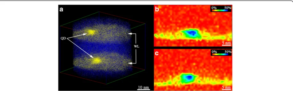
Figure 1a shows the APT data obtained from the fabri-cated needle of the sample. In atoms are shown as yellow dots and Ga atoms as blue dots (for a better visualization, only 20% of Ga atoms have been included, and none of the Al and As atoms). Our results show that the QDs (marked with arrows in the figure) are slightly asymmetric, with diameters of 9.5 ± 0.9 nm and heights of 5.6 ± 0.2 nm. Also, it should be highlighted that the APT data evidences that the QD in the second layer do not follow a vertical alignment with regard to the QD in the first layer. There is a misalignment of approximately 13° from the growth direction. Thus, our objective is to verify whether a strain analysis using FEM based on the APT data from the lower QD layer is able to predict this misalignment.
In distribution, where the dark blue area indicates the higher In concentration, corresponding to the core of the QD. The absence of a uniform composition gradient from the centre of the QD in different directions prevents from the accurate theoretical simulation of the QD composition required to perform a FEM simulation that approaches the real situation. This proves that atomic scale experi-mental data such as those obtained from APT are essential in order to obtain realistic predictions of the QD nucle-ation sites from FEM analysis that can be used in the de-sign of QD heterostructures for advanced devices.
In order to predict the nucleation site of the QD in the second layer, the chemical potential of the material during growth should be considered. In this case, the chemical potential has two major contributions: the one related to the surface energy and the one corresponding to the elastic strain. With regard to the first one, a previ-ous analysis of the structure by transmission electron microscopy has shown that the structure grows with a flat surface, as no undulations have been observed in the wetting layers or in the surface of the structure. Because of this, the surface energy is not expected to have a major effect in the chemical potential of the structure in the prediction of the nucleation sites because prior to the formation of the second layer of QDs, the wetting layer is flat, therefore this term is neglected. As a result, the elastic strain is expected to be the determining factor for the growth process. This parameter will be calculated in this work using FEM based in the APT data.
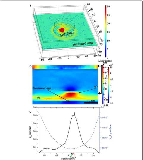
Figure 2a shows a slice of the input data, and the do-main sizes used in the FEM simulation, where the iso-surfaces corresponding to a composition of 30% In in the APT data have been drawn in red colour in order to better visualize the QD. In this schematic, the limits be-tween the APT data (corresponding to a cylindrical area because of the needle-shaped specimen, as mentioned earlier) and the simulated data added to avoid any
[image:3.595.61.538.89.238.2]alignment with the lower QD was also found in the ex-perimental APT data. However, in order to compare the deviations found in both cases, it is necessary to analyse the situation in the growth plane.
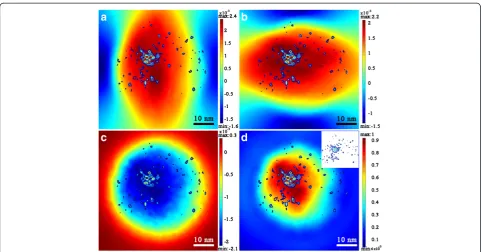
[image:4.595.58.540.88.628.2]Figure 3 shows 2D views of the strain maps calculated in the growth plane, at the surface of the barrier layer: (a) and (b) shows the strain in x and y directions (εxx and εyy), which are two perpendicular axes contained in
the growth plane, (c) showsεzz, and (d) shows the nor-malized SED. In order to compare the predictions calcu-lated by FEM with the experimental results obtained by APT, superimposed to these strain maps, we have in-cluded the APT data corresponding to the upper layer of QDs in the form of In concentration isolines, ranging from 25% In (dark blue) to 45% In (red), in steps of 5%. Also, in (d), we have included an inset showing a complete map of the APT data for clarity. As it can be observed in Figure 3a,b,c, there is a relatively wide area of similar strain where the QD would be favoured to grow, and the real QD is actually included in this area according to the APT data. Figure 3d shows the distribu-tion of the normalized SED, which represents a compen-dium of strain–stress in all directions ij as explained earlier, and which maximum value determines the most favoured localization of the QD [29]. In this map, the area favoured for the growth of the QD has a reduced size, but the actual QD is still included in this area ac-cording to the APT experimental data [14,19]. This re-sult shows that FEM using APT experimental data is an accurate tool for the prediction of stacked QD nucle-ation sites for structures where the strain component has a major effect in the chemical potential during growth. It should be mentioned that the eventual nucle-ation of the quantum dot is governed by a flux that drives surface adatoms from locations of higher to lower potential and the strain energy density critical value
(minimum or maximum depending on the sign conven-tion of SED [30]) is therefore the preferential site for nu-cleation. A more refined model would include additional parameters that typically affect the growth process, such as the surface energy [31] or kinetic effects [32]. These parameters are essential in the prediction of the nucle-ation sites of some semiconductor systems. For example, in InAs QWires, it has been reported that the stacking pattern is determined by the combined effect of strain and surface morphology on the growth front of the spa-cer layers [33]. In the structure considered in the present work, our results have shown that a simplified approxi-mation of the chemical potential considering only the strain component is valid for obtaining accurate results.
[image:5.595.57.540.87.339.2]On the other hand, our results have shown that the upper QD does not grow vertically aligned with the lower QD, but there is some deviation. Previous theoret-ical analyses have shown that this misalignment is, in part, related to the elastic anisotropy in the material [14], where the increase in the degree of anisotropy fa-vours the anti-correlated island growth [19]. It has also been reported that the QD base size and density have a strong influence on this misalignment [11], although the QD shape (truncated-pyramidal or lens-shaped) may not have a major effect in the strain at the surface of the capping layer [14]. These theoretical analyses are very useful for understanding the parameters that influence the QD nucleation sites. However, they have been Figure 3Strain and SED maps in the growth plane of the upper QD. (a)εxx,(b)εyy,(c)εzzand(d)normalized SED calculated in the surface
Conclusions
In conclusion, we have evaluated the accuracy of strain calculations by FEM using 3D atomic scale data obtained by APT for the prediction of the preferential nucleation sites of InAs stacked QDs. Our results by FEM have shown a very good agreement with our experimental ob-servations, showing that this is a very useful tool for the analysis of the strain distribution in semiconductor sys-tems. The combination of APT with FEM opens up the possibility of understanding the behaviour of complex semiconductor systems where strain plays a major role.
Abbreviations
APT:Atom probe tomography; FEM: Finite elements method; FIB: Focused ion beam; GaAs: Gallium arsenide; InAs: Indium arsenide; QDs: Quantum dots; SED: Strain energy density.
Competing interests
The authors declare that they have no competing interests.
Authors' contributions
JHS has participated in the design of the study, prepared the experimental specimens and carried out the APT analysis with SD, performed the FEM study, taken part in discussions and in the interpretation of the results, and written the manuscript. MH has participated in the FEM data analysis; she has supervised the research and revised the manuscript, and has taken part in discussions and in the interpretation of the results. SD has taken part in discussions and in the interpretation of the results. SIM has conceived the study; he has coordinated the work and the collaboration between groups, and he has participated in its design and supervised the manuscript. All the authors have read and approved the final manuscript.
Authors' information
JHS is a PhD student at the Universidad de Cádiz. MH is an Associate Professor at the Departamento de Ciencia de los Materiales e Ingeniería Metalúrgica y Química Inorgánica, Universidad de Cádiz. SD holds an Associate Professor at Université et INSA de ROUEN and he is the responsible of the Matériaux de la Microélectronique et de la Photonique (ER2MP) group. SIM is a full professor at the Departamento de Ciencia de los Materiales e Ingeniería Metalúrgica y Química Inorgánica, Universidad de Cádiz and the head of the Materials and Nanotechnology for Innovation group (INNANOMAT). This group belongs to the Institute of Electron Microscopy and Materials (interim stage) of the University of Cádiz.
Acknowledgements
This work was supported by the Spanish MINECO (projects TEC2011-29120-C05-03 and Consolider Ingenio 2010 CSD2009-00013), the Junta de Andalucía (PAI research group TEP-946 INNANOMAT), and METSA project. The authors greatly acknowledge J. Houard for discussion and help in APT analyses and Prof. C. R. Stanley from University of Glasgow for QD sample fabrication.
3. Lam AW, Ng TY:Electronic confinement in self-assembled quantum dots (SAQD) modeled with a new interfacial capping layer.Comp Mater Sci
2010,49:S54–S59.
4. Marti A, Cuadra L, Luque A:Quantum dot intermediate band solar cell.In
Conference Record of the Twenty-Eighth IEEE Photovoltaic Specialists Conference– 2000: September 15–22, 2000.Anchorage, Alaska, New York: IEEE; 2000:940–943. 5. You MH, Li ZG, Gao X, Qiao ZL, Wang Y, Liu GJ, Li L, Li M:Long wavelength strain-engineered InAs five stacks quantum dots laser diode growth by molecular beam epitaxy.Optik2013,124:1849–1851.
6. Kim JO, Sengupta S, Barve AV, Sharma YD, Adhikary S, Lee SJ, Noh SK, Allen MS, Allen JW, Chakrabarti S, Krishna S:Multi-stack InAs/InGaAs sub-monolayer quantum dots infrared photodetectors.Appl Phys Lett2013,102:011131. 7. Tersoff J, Teichert C, Lagally MG:Self-organization in growth of quantum
dot superlattices.Phys Rev Lett1996,76:1675–1678.
8. Holy V, Springholz G, Pinczolits M, Bauer G:Strain induced vertical and lateral correlations in quantum dot superlattices.Phys Rev Lett1999,
83:356–359.
9. Shoji Y, Oshima R, Takata A, Okada Y:The effect of spacer layer thickness on vertical alignment of InGaAs/GaNAs quantum dots grown on GaAs(3 1 1)B substrate.Phys E2010,42:2768–2771.
10. Hernandez-Saz J, Herrera M, Alonso-Alvarez D, Molina SI:Analysis of the 3D distribution of stacked self-assembled quantum dots by electron tomography. Nanoscale Res Lett2012,7:681.
11. Wang DL, Yu ZY, Liu YM, Lu PF, Han LH, Ye H, Guo XT, Feng H, Xin X:The structure transition from vertical alignment to anti-alignment of InAs/InP quantum dot multilayers.Solid State Commun2011,151:1266–1269. 12. Ouattara L, Ulloa JM, Mikkelsen A, Lundgren E, Koenraad PM, Borgstrom M,
Samuelson L, Seifert W:Correlation lengths in stacked InAs quantum dot systems studied by cross-sectional scanning tunnelling microscopy. Nanotechnology2007,18:145403.
13. Jin-Phillipp NY, Phillipp F:Strain distribution in self-assembled InP/GaInP quantum dots.J Appl Phys2000,88:710–715.
14. Pei QX, Quek SS, Guo JY, Lu C:Elastic fields in quantum dots arrays: a three-dimensional finite element study.Eng Anal Bound Elem2008,
32:309–317.
15. Sun C, Lu P, Yu Z, Cao H, Zhang L:Wetting layers effect on InAs/GaAs quantum dots.Phys B Condens Matter2012,407:4440–4445. 16. Liu YM, Yu ZY, Jia BY, Xu ZH, Yao WJ, Chen ZH, Lu PF, Han LH:Strain
distributions and electronic structure of three-dimensional InAs/GaAs quantum rings.Chin Phys B2009,18:4667–4675.
17. Cui K, Robinson BJ, Thompson DA, Botton GA:InAs quantum wire induced composition modulation in an In0.53Ga0.37Al0.10As barrier layer grown on an InP substrate.J Appl Phys2010,108:034321.
18. Willatzen M, Lassen B, Madsen S, Barettin D:Strain and piezoelectric effects in quantum-dot structures.InNumerical Simulation of Optoelectronic Devices (NUSOD) 11th International Conference: September 5–8, 2011.Rome: IEEE; 2011:167–168.
19. Quek SS, Liu GR:Effects of elastic anisotropy on the self-organized ordering of quantum dot superlattices.Nanotechnology2003,14:752–764. 20. Molina SI, Ben T, Sales DL, Pizarro J, Galindo PL, Varela M, Pennycook SJ,
Fuster D, Gonzalez Y, Gonzalez L:Determination of the strain generated in InAs/InP quantum wires: prediction of nucleation sites.Nanotechnology
2006,17:5652–5658.
22. Blavette D, Duguay S, Pareige P:Atom probe tomography: from physical metallurgy towards microelectronics.Int J Mater Res2011,102:1074–1081. 23. Duguay S, Philippe T, Cristiano F, Blavette D:Direct imaging of boron
segregation to extended defects in silicon.Appl Phys Lett2010,97:242104. 24. Muller M, Cerezo A, Smith GDW, Chang L, Gerstl SSA:Atomic scale
characterization of buried InxGa1−xAs quantum dots using pulsed laser
atom probe tomography.Appl Phys Lett2008,92:233115.
25. Beltrán AM, Marquis EA, Taboada AG, Ripalda JM, García JM, Molina SI:
Three dimensional atom probe imaging of GaAsSb quantum rings. Ultramicroscopy2011,111:1073–1076.
26. Hernandez-Saz J, Herrera M, Molina SI:A methodology for the fabrication by FIB of needle-shape specimens around sub-surface features at the nanometre scale.Micron2012,43:643–650.
27. Barettin D, Madsen S, Lassen B, Willatzen M:Computational methods for electromechanical fields in self-assembled quantum dots.Commun Comput Phys2012,11:797–830.
28. Semiconductor database of the Ioffe Physical Technical Institute, St. Petersburg, Russia.[http://www.ioffe.rssi.ru/SVA/NSM/Semicond/] 29. Liu YM, Yu ZY, Huang YZ:Dependence of elastic strain field on the
self-organized ordering of quantum dot superlattices.J Univ Technol Beijing2007,14:477–481.
30. Pei QX, Lu C, Wang YY:Effect of elastic anisotropy on the elatic fields and vertical alignment of quantum dots.J Appl Phys2003,93:1487–1492. 31. Korzec MD, Münch A, Wagner B:Anisotropic surface energy formulations
and their effect on stability of a growing thin film.Interface Free Bound
2012,14:545–567.
32. Zhao C, Zhao M, Wang Y, Lv AJ, Wu GM, Xing GJ:Monte Carlo simulation of the kinetics in the growth of semiconductor quantum dots.Mod Phys Lett B2011,25:465–471.
33. Cui K, Robinson BJ, Thompson DA, Botton GA:Stacking pattern of multi-layer In As quantum wires embedded in In0.53Ga0.47−xAlxAs matrix layers grown
lattice-matched on InP substrate.J Cryst Growth2010,312:2637–2646.
doi:10.1186/1556-276X-8-513
Cite this article as:Hernández-Sazet al.:Strain analysis for the prediction of the preferential nucleation sites of stacked quantum dots by combination of FEM and APT.Nanoscale Research Letters20138:513.
Submit your manuscript to a
journal and benefi t from:
7 Convenient online submission 7 Rigorous peer review
7 Immediate publication on acceptance 7 Open access: articles freely available online 7 High visibility within the fi eld
7 Retaining the copyright to your article