International Journal of Emerging Technology and Advanced Engineering
Website: www.ijetae.com (ISSN 2250-2459,ISO 9001:2008 Certified Journal, Volume 5, Issue 8, August 2015)
357
A 11GHz Narrow Band Pass Filter Design with Lumped
Elements, EM Sight and AXEIM Techniques
Pramod K B
1, Kumaraswamy H.V
2, Kamala C
3, Praveen K B
41PhD Student of JAIN University & Asst Prof. in EXTC Dept. at MCT’s RGIT, Mumbai 2Prof and HOD at Dept of Telecommunication, R. V. C. E, Bangalore, India
3Dept of Medical Electronics, 4Dept of Telecom, Dr. Ambedkar Institute of Technology, India
Abstract— this paper presents the Design, Simulation, Analysis and characterization of Band pass filter based on three different techniques. First one is only lumped element design, second one printed micro strip PTFE on 15 mil Alumina substrate and finally with AXEIM. Simulations show a comparison between Lumped element design, a pure EM simulation with EM Sight and a more efficient hybrid approach that combines EM analysis (using X-Models) with conventional circuit simulations and both approaches match the measured data and finally with AXEIM. Furthermore, the proposed paper as three different band pass filter designs, Tuning and Optimization of the design is carried out using AWR Microwave office tool. Design is done based on wizards available in the tool with single layer MMIC technique.
Keywords— EM Simulation, EM sight, X-Models, Band pass filter, Transformed Radial Stubs, Micro strip ,AWR MWO and PTFE.
I. INTRODUCTION
Band pass filters are essential building blocks in communication system designs. It can reduce the harmonic and spurious emissions for transmitters, and may improve the rejection of interferences for receivers. As an important component in the multiband transceiver, a multiband band pass filter (BPF) with compact size, planar configuration, and high performance has garnered a great deal of attention to meet these requirements[4]. The rapid growth in commercial microwave technology, varies of microwave communication system had been developed [13]. Hence, Micro strip filters play important roles in many RF or microwave applications. Emerging applications such as wireless communications continue to challenge RF/microwave filters with ever more stringent requirements higher performance, smaller size, lighter weight, and lower cost. Nowadays, most of mmW band pass filters (BPFs) are mainly fabricated with Low Temperature Co-fired Ceramic (LTCC) [2].
Several research topics in microwave filter technology, including computer-aided design (CAD) tools, full-wave analysis, new structures and configurations, low-temperature co-fired ceramics (LTCC), high-low-temperature superconductor substrate, liquid crystal polymer (LCP), micromachining, multilayer monolithic and associated technologies, have stimulated the rapid development of advanced filters in future wireless communication systems. Many novel filters with high performance and small size have been demonstrated. Moreover, the multiband filters have more attractive attentions in multiservice, multichannel, and/or long-term evolution (LTE) of 3GPP's universal mobile telephone system (UMTS). The physical dimension is becoming crucial issues particularly for communication devices which have small size [5] and needs a planar wideband BPF with single plane configuration, compact size and high electrical performance simultaneously [6].
II. MICROWAVE FILTER TECHNOLOGIES
In general, most RF and microwave filters are most often made up of one or more coupled resonators, and thus any technology that can be used to make resonators can also be used to make filters. The unloaded quality factor of the resonators being used will generally set the selectivity the filter can achieve by
Micro strip filters
Low-Temperature Co-fired Ceramics (LTCC)
Liquid Crystal Polymer (LCP)
High Temperature Super Conductivity (HTS) filters
International Journal of Emerging Technology and Advanced Engineering
Website: www.ijetae.com (ISSN 2250-2459,ISO 9001:2008 Certified Journal, Volume 5, Issue 8, August 2015)
358
The second problem is these narrow bands are not easily obtainable with conventional filter implementations. So we have to go for the distributed micro strip designs which use the conventional model blocks to achieve a best outcome.The targeted measurement in this work is to design Narrow band Bandpass filter with 11.65 GHz centre frequency. To achieve low Insertion loss of -5dB or better, at the operating Bandwidth 10.8GHz-12.5GHz with Pass Band Ripple of ±0.2dB. To restrict Return loss to -12dB which in turn responsible to achieve better VSWR of 14dB with high Rejection of -20db @ 10.625GHz & 12.675GHz and -50dB @ 10.05GHz & 13.25GHz. To generate Gerber file to the designed filter on PTFE laminate substrate within the given dimensions of W×L×H respectively as 6×35×4 (units in mm).
III. RESEARCH AND COLLECTED DATA
JinXu and WenWu [13] presents a new type of dual-mode dual-band BPF by using a single micro strip QMR. Two pairs of transmission are produced in the filters to improve the pass band selectivity. Kaixue Ma [11] given a design approach for a filter with ultra-wide-band rejection, compact size band pass filter (BPF) topology design based on the transformed radial stub (TRS) cell embedded resonator (CER) is proposed for the high-performance filter design. JinXu, WenWu [4] presents a new class of dual-, tri-, and quad-band BPFs by using the proposed directly coupled OSLSSIR. The TZs produced by two identical open stubs of OSLSSIR divide multiple resonant modes of proposed OSLSSIR into multiple groups.
However the above designs has their own pros and cons but this paper presents designing and simulation of micro strip band pass filters by using EM Simulation models by using AWR Microwave Office simulation program developed by Applied Wave Research USA. In the design of a Microwave filter using micro strips two types of design approaches are taken. First, transforming the lumped element design to equivalent planar structure. Second, using micro strip resonators and the concepts of immitance inverter. For the band pass design the second approach is used.
After understanding clearly about the filter parameters I can brief the few main filter parameters which are necessary for my design as shown in the table 1 below
TABLEI
FILTER PARAMETERS BRIEFED TO UNDERSTAND HOW THE FILTER PARAMETERS ARE INTERLINKED.
Order
‘N’ Rejection/ Attenuation
Insertion loss
BW ‘Q’ Group Delay
More More More Less More More
A. EM Simulation
Electromagnetics (EM) has today become a critical part of the microwave design cycle. Typical products resulting from the new EM-based methodologies from Dielectric Labs [16]. While these filters look like normal two- and three-port structures, the EM analyses for these filters using the new design methodologies (topological partitioning, functional partitioning, and tuning methodology) typically include dozens of extra ports. Properly included, these extra ports reduce the design process from weeks and months to, literally, days. In fact, analysing these filters as simple two or three ports is now sometimes a waste of time. As we describe the new design cycle below, we will see why this is happening. All of these new methodologies effectively amount to producing precisely and quickly
tuneable EM analyses.
Today, instead of building the circuit, the layout is passed to an EM analysis tool. For aggressive designs, the circuit still does not meet requirements. The redesign takes place entirely on the computer. We just modify the polygons of the layout. A complete redesign and EM analysis of a moderately complex circuit can now take a week or so, instead of the few months sometimes required by design-fabricate-measure. Because of the EM analyses, we know that our first layout will not meet requirements.
International Journal of Emerging Technology and Advanced Engineering
Website: www.ijetae.com (ISSN 2250-2459,ISO 9001:2008 Certified Journal, Volume 5, Issue 8, August 2015)
359
IV. FILTER IMPLEMENTATIONThe proposed band pass filter (BPF) topology design is based on the transformed radial stub (TRS) cell embedded resonator (CER) is for the high-performance filter design.
A. Filter Realization/Design Procedure: 1) Insertion loss method:
The insertion-loss method begins with a complete specification of a physically realizable frequency characteristic, and from this a suitable filter schematic is synthesized.
The output of an ideal filter would be the same as its input in the pass band, whereas it would be zero in the stopband. The phase response of this filter must be linear to avoid signal distortion. In reality, such circuits do not exist and a compromise is needed to design the filters. However, the transfer characteristics of this circuit cannot be shaped as desired. On the other hand, the insertion-loss method provides ways to shape pass- and stop bands of the filter, although its design theory is much more complex.
The power-loss ratio of a two-port network is defined as the ratio of the power that is delivered to the load when it is connected directly at the generator to the power delivered when the network is inserted between the two. In other words,
Where Γ is the reflection coefficient looking into the filter. The power-loss ratio, PLR, expressed in decibels, is generally known as the insertion loss of the network. It can be proved that |Г (ω) |2 must be an even function of ω for a physically realizable network. Therefore, polynomials of ω2 can represent it as follows.
And
Where f1 (ω2) and f2 (ω2) are real polynomials in ω2.
Alternatively, the magnitude of the voltage gain of the two-port network can be found as
Hence, if PLR is specified, Г(ω) is fixed. Therefore, the insertion-loss method is similar to the impedance-matching methods.
Traditionally, the filter design begins with a lumped-element low-pass network that is synthesized by using normalized tables. It is subsequently scaled to the desired cutoff frequency and the impedance. Also, the low-pass prototype can be transformed to obtain a high-pass, a band pass, or a bandstop filter. These lumped-element filters are used as a starting point to design the transmission line filter. In this section I present the design procedure for two different types of lumped-element low-pass filters. It is followed by the transformation techniques used to design high-pass, band pass, and bandstop filters.
B. Chebyshev Filter
A filter with a sharper cut-off can be realized at the cost of flatness in its pass band. Chebyshev filters possess ripples in the pass band but provide a sharp transition into the stop band. In this case, Chebyshev polynomials are used to represent the insertion loss. Mathematically,
Where ζ is a constant, is normalized frequency, and
TN(ω) is a Chebyshev polynomial of the first kind and degree N. Figure I shows the frequency response of a typical Chebyshev filter for N = 7. It assumes that ripples up to −3 dB in its pass band are acceptable. A comparison of this characteristic to that for a seventh-order Butterworth filter has a much sharper transition from pass band to stopband. However, it is achieved at the cost of ripples in its pass band.
As before, the insertion loss of a Chebyshev filter is found as follows:
International Journal of Emerging Technology and Advanced Engineering
Website: www.ijetae.com (ISSN 2250-2459,ISO 9001:2008 Certified Journal, Volume 5, Issue 8, August 2015)
360
α is the ripple amplitude in decibels. The order N (and hence, number of elements) of a Chebyshev filter can be found from its characteristics as follows:
Where IL is required insertion loss in decibels at a specified frequency ω.
FIGURE ICHARACTERISTICS OF A LOW-PASS CHEBYSHEV FILTER FOR
N=7
V. FILTER IMPLEMENTATION USING LUMPED ELEMENTS
Before going into the desired distributed implementation of the given filter first we have to design using the lumped elements and check the response of the filter for the given specifications. The components used in lumped design are extracted from the tool using their id‘s directly searching in the elements search option available in the tool bar or by browsing the elements menu. The components used for the design here is series LC resonators and the parallel LC resonators. The source and load resistors used are 50Ω and the input/output port impedance is also 50Ω which are primarily available in the components.
FIGURE IILUMPED ELEMENT DESIGN BY USING CHEBYSHEV FILTER COEFFICIENT
Based on filter coefficients of Chebyshev filter with 0.1 dB ripple are 1.3860, 1.3938, 2.3093, 1.5340, 2.3728, 1.5340, 2.3093, 1.3938, 1.3860, 1.0000 low pass filter has been designed and later by using transformation techniques the band pass filter is performed in AWR tool whose schematic is display below.
FIGURE IIIRETURN LOSS RESPONSE OF LUMPED ELEMENT DESIGN.
The Return loss plot for the Lumped element Simulation design is as shown in the figure 3 which is having good values at side frequencies about -60dB and at centre frequency around -30dB.
1) Schematic Responses
FIGURE IV SCHEMATIC RESPONSE AFTER LUMPED ELEMENT DESIGN USING COUPLED LINES.
FIGURE VINPUT AND OUTPUTVSWR RESPONSE OF LUMPED ELEMENT DESIGN.
International Journal of Emerging Technology and Advanced Engineering
Website: www.ijetae.com (ISSN 2250-2459,ISO 9001:2008 Certified Journal, Volume 5, Issue 8, August 2015)
361
FIGURE VIINPUT AND OUTPUTVSWR RESPONSE OF LUMPEDELEMENT DESIGN.
The Rejections plot of the lumped element design is as shown in the figure VI. The Stop band Rejections at the skirts of the filter response is meeting with the first requirements of the -60dB to -80dB rejection as mentioned in the requirements specifications
FIGURE VII2D LAYOUT OF THE COMPLETE HAIRPIN FILTER.
The dimensional layout of the Hairpin filter designed is as shown in the figure. The dimensions are shown in the figure and all the dimensions are in ‗mils‘.
FIGURE VIIIGROUP DELAY OF THE LUMPED ELEMENT DESIGN.
Group delay is the significant measurement which is restricted here up to +/- 2ns which acceptable value for the filter.
B. EM Sight
The Insertion loss plot of an EM Simulation Hairpin filter design.
The response is in violating the agreement with 1dB bandwidth criteria this is shown by adding the horizontal marker line for 1dB. One more criteria for my design is the pass band ripple as I mentioned in the problem statement section. The following figure shows the results of EM sight design which is having ripples in pass band but low rejection in pass band but input VSWR is not good.
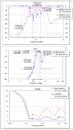
FIGURE IX INSERTION,RETURN LOSS AND VSWR RESULTS OF EM
[image:5.612.57.282.126.276.2] [image:5.612.317.571.217.659.2] [image:5.612.55.284.458.612.2]International Journal of Emerging Technology and Advanced Engineering
Website: www.ijetae.com (ISSN 2250-2459,ISO 9001:2008 Certified Journal, Volume 5, Issue 8, August 2015)
362
FIGURE X3D LAYOUT OFEM SIGHT DESIGN.The figure X shows the 3D layout of the EM Extracted Hairpin filter. The external shielding is done to avoid a parasitic coupling effects occurring during EM Simulation of the circuit design. Depending on the area constrains given in the specification we have given the height of the shield to be 100 mil.
FIGURE XICOMPLETE SCHEMATIC OFEM SIGHT DESIGN.
FIGURE XIII2D LAYOUT OFEM SIGHT DESIGN.
Corresponding schematic and layout is performed with unified model in AWR AXIEM and which is corrected with all layout design rules.
FIGURE XIVGROUP DELAY OFEM SIGHT DESIGN.
The Group Delay Response of the EM Simulation of Hairpin filter design is as shown in figure XIV. The Group delay has to be measured at the upper and lower cutoff frequencies more precisely.
FIGURE XVGROUP DELAY OFEM SIGHT DESIGN.
The EM Extraction layout is as shown in the figure XV. The dimensions are almost as same as the schematic and a small change is done to meet the design specifications. Because of the high frequency range of the filter and because of the coupling from the input to the output which is included in the EM Models there may be certain loss in the specification met in schematic. The Schematic is ideal there, because it has no such parasitic effects. Thus to achieve the specification certain tuning and optimization is even done after EM simulation too. Hence there is a change in the dimensions compared with the schematic. In the EM extraction we can add the annotations available to the current density, synchronization with the mesh and many more.
International Journal of Emerging Technology and Advanced Engineering
Website: www.ijetae.com (ISSN 2250-2459,ISO 9001:2008 Certified Journal, Volume 5, Issue 8, August 2015)
363
FIGURE XVIGROUP OF COMPLETE RESULTS AND RESULTS OF ONLY
AXEIM DESIGN.
VI. OBSERVATIONS
The design of the 11.65GHz Band pass Hairpin filter on Ceramic filled PTFE Laminate is designed and simulated using the AWR MWO tool. The results of lumped design, EM Simulation, AXIEM are briefly summarized and compared with each other in the Summary table as shown above. The design shows the good agreement with the distributed Hairpin design and some of the parameters are eventually improved than the Lumped design too. The EM Simulation of the Hairpin design is slightly deteriorated because of the higher frequency design. The shifting of the operating band after EM simulation of the Hairpin schematic is overcome in my design using the Radial stubs
instead of the MOPEN in the design. So this design seems to be unique compared with the other designs on single layer micro strip technology done so far.
VII. SUMMARY
COMPARISON BETWEEN LUMPED,HAIRPIN AND EM SIMULATED
FILTERS
Parameters Lumped
Filter
AXIEM EM
Simulation
Start Frequency 10.8 GHz 10.8 GHz 10.8 GHz
Stop Frequency 12.5 GHz 12.5 GHz 12.5 GHz
Insertion Loss @ (11.65GHz) - -5 dB
-7.25 dB -0.9856 dB -0.5337
Return Loss @ (11.65GHz) – 12 dB
-10.09 dB -14 dB -17.71 dB
Attenuation @ (10.625 & 12.675 GHz) – 20 dB min.
31.19 & -20.79 dB
20.79 & -20.54 dB
20.83 & -20.25 dB Attenuation @
(10.05 & 13.25 GHz) – 50 dB min
-68.87 & 59.45 dB
48.05 & -45 dB
30.76 & -32.76 dB
Passband Ripple - ± 0.2 (in dB)
± 0.6 ± 0.2 ± 0.75
VSWR IN/OUT over Passband – 1.6
International Journal of Emerging Technology and Advanced Engineering
Website: www.ijetae.com (ISSN 2250-2459,ISO 9001:2008 Certified Journal, Volume 5, Issue 8, August 2015)
364
VIII. CONCLUSIONThe design of hairpin filter and its simulation was successfully done in this proposed work. After obtaining the appropriate order of the filter, the values of the odd and even impedances were computed using the admittance inverter parameters. Using transmission line calculator software, the values of the line width and spacing between resonators were also obtained. It was then optimized using the Optimization tool of AWR to compensate for the reduced coupling between resonators. The design was optimized by making use of the tool.
Using a ceramic-filled substrate significantly decreased the final size of the filter due to its high dielectric constant. Another important factor that contributed to the decrease in size was the low thickness of the dielectric. For applications that require small size and stable dielectric constant, it is recommended to use high dielectric constant and thin dielectric ceramic-filled PTFE laminates.
IX. FUTURE IMPROVEMENT IN THE DESIGN
The Hairpin design presented here can be further enhanced by designing the same for the reconfigurable bandwidths. This means that here we have designed for the single frequency that is 11.65 GHz, the reconfigurable bandwidths in the sense we can design the filter to operate in two or more frequencies when the particular frequency has been selected. This can be made by cascading the two filters and by using the diodes we can switch on the particular frequency that we need to operate [2].
The design is showing some spurious response in the second and the third harmonics which does not affect the design but important at the higher frequency. This can be eliminated by fine tuning or optimizing or by using the harmonic stubs at the input and the output side of the filter. Since area is the constraint, harmonic stubs are not used in the design. The harmonic stubs can be used in the design to eliminate the second and third harmonics when the area is not a constraint in the design.
REFERENCES
[1] Hui Wang, Kam-Weng ,Sut-KamHo, Wei Kang,and WenWu, ―Design of Ultra-Wideband Bandpass Filters With Fixed and Reconfigurable Notch Bands Using Terminated Cross-Shaped Resonators‖ IEEE TRANSACTIONS ON MICROWAVE THEORY AND TECHNIQUES, VOL. 62, NO. 2, FEBRUARY 2014, Pg:252-265
[2] Sai Wai Wong, KaiWang, Zhi-NingChen, Qing-Xin Chu, ―Design of Millimeter-Wave Bandpass Filter Using Electric Coupling of Substrate Integrated Waveguide (SIW)‖ IEEE MICROWAVE AND WIRELESS COMPONENTS LETTERS, VOL. 24, NO. 1, JANUARY 2014 , 1531-1309 © 2013 IEEE Pg : 26-28
[3] K. Rabbi and D. Budimir ―Miniaturised Sharp Rejection Bandpass Filter with Reconfigurable Bandwidth for UWB Applications‖ Proceedings of the 43rd European Microwave Conference,
978-2-87487-031- -1026
[4] JinXu, WenWu, and Chen Miao,‖ Compact Microstrip Dual-/Tri-/Quad-Band Bandpass Filter Using Open Stubs Loaded Shorted Stepped-Impedance Resonator‖ IEEE TRANSACTIONS ON MICROWAVE THEORY AND TECHNIQUES, VOL. 61, NO. 9, SEPTEMBER 2013 , Pg : 3187-3199
[5] Achmad Munir, Ivan Pradibta, Mohammad Ridwan Effendi, ―Microstrip-based Ultra-Wideband Composite BPF with Short-circuited Stubs‖ 978-1-4799-0545-4/13/$31.00 ©2013 IEEE. [6] Jin Xu, Yu-Xue Ji, Chen Miao,and WenWu, ―Compact
Single-/Dual-Wideband BPF Using Stubs Loaded SIR (SsLSIR)‖ 1531-1309/$31.00 © 2013 IEEE , IEEE MICROWAVE AND WIRELESS COMPONENTS LETTERS, VOL. 23, NO. 7, JULY 2013 , Pg: 338-340
[7] Muhammad Imran Nawaz, Muhammad Kashif, Abdul Mueed, Zhao Huiling, ―Compact Wideband Microstrip Bandpass Filter for IF Stage of Millimeterwave Systems‖ Proceedings of 2013 10th International Bhurban Conference on Applied Sciences & Technology (IBCAST) Islarnabad, Pakistan, 15th - 19th January, 2013, Pg 393-397
[8] Guo-Min Yang ,JingWu ,JingLou , Ming Liu , and Nian X. Sun ―Low-Loss Magnetically Tunable Bandpass Filters With YIG Films‖ 0018-9464 © 2013 IEEE, IEEE TRANSACTIONS ON MAGNETICS, VOL. 49, NO. 9, SEPTEMBER 2013,
[9] Hsin-Chih Kuo, IEEE,Han-LinYue, Ya-WenOu, Chien-Chih Lin and Huey-Ru Chuang, ―A 60-GHz CMOS Sub-Harmonic RF Receiver With Integrated On-Chip Artificial-Magnetic-Conductor Yagi Antenna and Balun Bandpass Filter for Very-Short-Range Gigabit Communications‖ 0018-9480/$31.00 © 2013 IEEE IEEE TRANSACTIONS ON MICROWAVE THEORY AND TECHNIQUES, VOL. 61, NO. 4, APRIL 2013, Pg: 1681 - 1691 [10] Haiwen Liu, Baoping Ren, Xuehui Guan, Jiuhuai Lei, and Shen Li ,
―Compact Dual-Band Bandpass Filter Using Quadruple-Mode Square Ring Loaded Resonator (SRLR)‖ IEEE MICROWAVE AND WIRELESS COMPONENTS LETTERS, VOL. 23, NO. 4, APRIL 2013, 1531-1309/$31.00 © 2013 IEEE, Pg 181-183 [11] Kaixue Ma, Shouxian Mou, Keping Wang, Kiat Seng Yeo,‖
Embedded Transformed Radial Stub Cell for BPF With Spurious-Free Above Ten Octaves‖ IEEE TRANSACTIONS ON COMPONENTS, PACKAGING AND MANUFACTURING TECHNOLOGY, VOL. 3, NO. 9, SEPTEMBER 2013, 2156-3950 © 2013 IEEE, Pg: 1597-1603
[12] Meng-Jian Bao, Xu-Guang Wang, Young-Ho Cho, and Sang-Won Yun, Dong-Chul Park, ―Design of A Four-Pole Wide Stopband Bandpass Filter Using Combined Quarter-wavelength Resonators and Stub-Loaded SIR‖ Proceedings of APMC 2012, Kaohsiung, Taiwan, Dec. 4-7, 2012, Pg:115-117
[13] JinXu, WenWu, and Chen Miao, ―Compact and Sharp Skirts Microstrip Dual-Mode Dual-Band Bandpass Filter Using a Single Quadruple-Mode Resonator (QMR)‖ , IEEE TRANSACTIONS ON MICROWAVE THEORY AND TECHNIQUES, VOL. 61, NO. 3, MARCH 2013, 0018-9480/$31.00 © 2013 IEEE, Pg : 1104-1113 [14] Ghulam Mehdi, Hu Anyong, Miao Jungang, ―Millimetre-wave All
International Journal of Emerging Technology and Advanced Engineering
Website: www.ijetae.com (ISSN 2250-2459,ISO 9001:2008 Certified Journal, Volume 5, Issue 8, August 2015)
365
[15] C. Tan, H. Wang, G. Yang, J.-Z. Zhao, ―A Balun-BPF Using Coupled Lines with Capacitive Loads‖, ICCP2012 IEEE Proceedings, Pg: 73-75
[16] Cheng-Ying Hsu,Chu-YuChen, and Huey-Ru Chuang , ―Microstrip Dual-Band Bandpass Filter Design With Closely Specified Passbands‖ IEEE TRANSACTIONS ON MICROWAVE THEORY AND TECHNIQUES, VOL. 61, NO. 1, JANUARY 2013, 0018-9480/$31.00 © 2012 IEEE, Pg: 98-106
[17] Girdhari Chaudhary, Yongchae Jeong, and Jongsik Lim,‖ Dual-Band Bandpass Filter With Independently Tunable Center Frequencies and Bandwidths‖ IEEE TRANSACTIONS ON MICROWAVE THEORY AND TECHNIQUES, VOL. 61, NO. 1, JANUARY 2013, Pg:107-116
[18] Ahmet Kenan Keskin and Hakan P. Partal, ―An UWB High-Q Bandpass Filter with Wide Rejection Band using Defected Ground Structures‖ 978-1-4577-2032-1/12/$26.00 © 2012 IEEE, ICUWB 2012, Pg:99-102
[19] Sergio c. Pires, Pedro M. Cabral, Jose C. Pedro ―A Carrier-Burst Transmitter Implementation: Design of Bandpass filter and Amplifier-BPF Connection‖ 978-1-4673-2949-1/12/$31.00 ©2012 IEEE
[20] Runqi Zhang, and Lei Zhu,‖ Synthesis Design of a Wideband Bandpass Filter with Inductively Coupled Short-Circuited Multi-Mode Resonator‖ IEEE MICROWAVE AND WIRELESS COMPONENTS LETTERS, VOL. 22, NO. 10, OCTOBER 2012, 1531-1309/$31.00 © 2012 IEEE, Pg: 509-511
[21] Sohail Khalid, Wong Peng Wen and Lee Yen Cheong,‖ Synthesis and Design of Four Pole Ultra-Wide Band (UWB) Bandpass Filter (BPF) Employing Multi-Mode Resonators (MMR)‖, 978-1-4673-1088-8/12/$31.00 ©2012 IEEE,
[22] Xuehui Guan, Bin Wang, Xiaoyan Wang, Haiwen Liu, Ye Yuan, and Xiaoyan Zhang, ―Design of a Dual-Mode Substrate Integrated Waveguide Filter with Slot Line Perturbation‖ 978-1-4673-2185-3/12/$31.00 ©2012 IEEE
[23] D. Jung, J. Hansen and K. Chang, ―Miniaturised bandpass filter using dumb-bell-shaped slot resonator‖ ELECTRONICS LETTERS 19th January 2012 Vol. 48 No. 2
[24] Xu-Guang Wang, Young-Ho Cho , and Sang-Won Yun, ―A Tunable Combline Bandpass Filter Loaded With Series Resonator‖ IEEE TRANSACTIONS ON MICROWAVE THEORY AND TECHNIQUES, VOL. 60, NO. 6, JUNE 2012, 0018-9480/$31.00 © 2012 IEEE, Pg:1569-1576
[25] Masoud Sabaghi, M.Kouchaki , A.Rostami, H.Shamsoskouie, M.Rahnama, ―Design and simulation of Low-Noise Bandpass filter by using Active Capacitance Circuit‖ 2012 IEEE 8th International Colloquium on Signal Processing and its Applications, 978-1-4673-0961-5/12/$31.00 ©2012 IEEE, Pg:1-4
AUTHOR‘S PROFILE
Mr. Pramod K B was born in Mysore, Karnataka, India in 1989. He is currently working as Assistant Professor in MCT‘s RGIT, Mumbai and also working towards PhD degree at JAIN University, Bangalore in Electronics Engineering. He received his B.E degree in Electronics and Communication from Dr. Ambedkar Institute of Technology, Bangalore Visvesvaraya Technological University in 2010, M.Tech degree in R F Communication from Jain University, Bangalore, in 2012 and He worked as R F Design trainee at Icon Design and Automation Pvt LtD and as visiting research scholar at University of Concordia, Montreal, Quebec, Canada. His research includes Design, Characterization And Optimization Of RF Passive Devices , Board Level Tuning And Optimization Of Matching Networks, Low Noise Amplifier , Power Amplifier, Circuit Linearization And High-Efficiency Design Techniques, Circuit Instability And Strategies
E-mail: [email protected] [email protected]
Prof. Dr. Kumaraswamy H.V is currently working as Professor & HOD in the Dept of Telecommunication Engineering, RVCE, and Bangalore. His research interests are Digital Signal Processing, Adaptive Signal Processing and Communication. He has got PhD from Visvesvaraya Technological University for the research work on Smart antenna System using Dielectric lens. He is the author of the book titled "Signals & Systems" Published by: Scitech Publication, Chennai, ISB No.8188429260.
E-mail: [email protected]