International Journal of Emerging Technology and Advanced Engineering
Website: www.ijetae.com (ISSN 2250-2459,ISO 9001:2008 Certified Journal, Volume 5, Issue 11, November 2015)
275
Comparative Analysis of Operations of Different
Circuits of Analogue Comparator in CMOS
Technology
Khulesh Sahu
1, Asst. Prof. Ravi Tiwari
2 1Student, Raipur, India2Asst Prof. Bhilai, India
Abstract—Comparator is one of the most essential analog
circuits required in many analog integrated circuits. It is used for the comparison between two similar or different electrical signals with reference. The design of Comparator becomes an essential issue when technology is scaled down. Due to the non-linear behavior of threshold voltage (VT) when the scale of technology is reduced, performance of Comparator is affected. Many versions of comparator are proposed to acquire enticing output in sub-micron and deep sub-micron technologies. The selection of particular topology is dependent upon the requirements and application. In this we will simulate all types mentioned types of comparators and analyze them on the basis of different characteristics of comparator like : power dissipation , offset voltage , delay, speed and no. of transistor used. The simulated in HSPICE.
Keywords— double tail latch type comparator, dynamic
comparator, pre amplifier based comparator, dual tail double rail type comparator, power dissipation, offset voltage, delay, speed, no. of transistors used ,low power analogue design.
I. INTRODUCTION
In electronics, Operational amplifier is designed to be used with negative feedback. It can be also used as comparator in open loop configuration. On the other hand, Comparator is especially designed for open loop configuration without any feedback. Hence it is the second most widely used device in electronic circuits after Opamp.(3) Comparators are mostly used in analog-to-digital converter (ADCs). In the conversion process, the sampled signal is applied to a number of comparators to determine the digital equivalent of the analog value. Apart from that, comparators are used in peak detectors, zero crossing detectors, BLDC operating motors, switching power regulators
II. DEFINITION
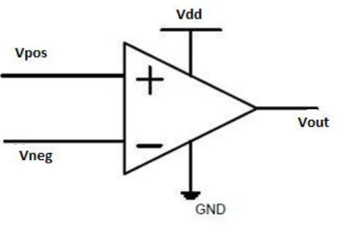
[image:1.612.329.572.269.435.2]Comparators are the device that compares two analogue voltages or currents and switches it output to indicate which one is larger.
Figure I Opamp Based Comparator
If Vpos is at a greater potential than Vpos, then the output Vout of the comparator is logic 1 and when Vpos is at a potential less than Vneg, then the output is at logic 0.
If we apply a pulse voltage at Vpos and a DC reference voltage at Vneg, the output is logic 1 when the pulse amplitude is greater than the reference voltage.(5) The figure is shown below. Thus a comparator compares two input analog value and gives binary output. In ideal case, binary signals can have two values at any point. But actually there is a transition region between the two binary states. For a comparator, it is important to pass quickly through that transition region. Basically comparators can be divided into two types. First are the Open loop comparators, which are nothing but OPamps. The second type is regenerative comparators. Regenerative comparators use positive feedback for the comparison of magnitude between two signals(5)
International Journal of Emerging Technology and Advanced Engineering
Website: www.ijetae.com (ISSN 2250-2459,ISO 9001:2008 Certified Journal, Volume 5, Issue 11, November 2015)
276
Also we have to minimize the power consumption by using smaller feature size processes. However when we move towards power consumption minimization, the process variations and other parameters will greatly affect the overall performance of the device. Now comparators are used in ADCs and ADCs.
In this project paper .preparing a table of comparators which give information of all types of comparator, which can help designer to choose better comparator for their design„s parameter and there requirements. The different parameter has compared as per information collected.,along with comparing the comparator, the designing of low power comparator designed and simulated in HSPICE.
III. DIFFERENT COMPARATOR
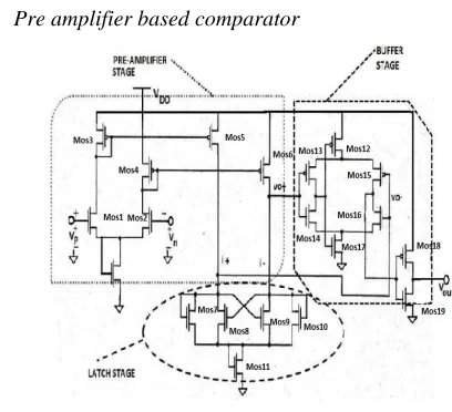
[image:2.612.58.262.310.496.2]A. Pre amplifier based comparator
Figure II Pre amplifier based comparator
Operation: The figure shows the preamplifier based comparator. The comparator has three stages: 1) the input preamplifier stage, 2)a latch stage, and 3)an output buffer stage.(5)
The preamplifier stage is fundamentally a differential amplifier with active loads. The Pre amp stage (or stages) amplifies the input signal to improves the comparator sensitivity and keep apart the input of the comparator from switching noise or kickback noise so it reduces noise coming from the regenerative feedback stage. It also can decrease input offset voltage.
The sizes of Mosl and Mos2 are set by taking into account the diff-amp transconductance and the input capacitance. The transconductance schedules the gain of the stage.
While the size of Mosl and Mos2 determines the input capacitance of the comparator. Here gm1= gm2. The regenerative feedback latch stage is applied to determine which of the input signals are larger and extremely amplifies their difference. It takes regenerative feedback from the cross gate connection of Mos8 and Mos9. Consider i+ >> i- so that Mos7 and Mos9 are ON and Mos8 and Mos10 are OFF. Here also β of Mos7= β of Mos10=βa and β of Mos8= β of Mos9=βb for which vo- slightly equals to 0V and v0+ is If we start to increase current i- and decrease current i+, when drain to source voltage of Mos9 is equal to the threshold voltage, Vt of Mos8, switching occurs. At this point Mos8 takes current away from Mos7 which reduces drain to source voltage of Mos7 and Mos9 goes off. If we assume that maximum value of v+ or v- is equal to 2Vt, then under these situations Mos8 and Mos9 operate in cut-off or triode region in steady state conditions. Then voltage over Mos9 becomes Vt and Mos9 goes to saturation and current of Mos9 this is the point at which switching occurs; that is Mos9 turns off and Mos8 goes on. If βa= βb , then switching occurs when , i+ and i-, are be equal. A same type of analysis of enhancing current i+ reducing current i- results in the output buffer, the final product of this comparator, it gives a full scale digital level output (logic 0 or logic 1) from the output of latch stage .
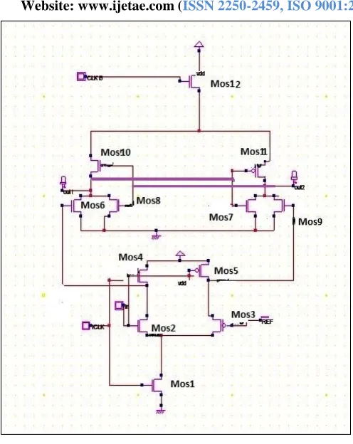
B. Double-Tail Latch Type Comparator:
The figure III shows the schematic of the Double-Tail Latch type Voltage Sense Amp.
International Journal of Emerging Technology and Advanced Engineering
Website: www.ijetae.com (ISSN 2250-2459,ISO 9001:2008 Certified Journal, Volume 5, Issue 11, November 2015)
[image:3.612.48.296.119.431.2]277
Figure III Double-Tail Latch Type Comparator
Operation: During rest phase when clk=0V, M4 and M5 charges to VDD which in turn charges Ni nodes to VDD. Hence Mos6 and Mos9 goes on and discharges output nodes to Ground. In evaluation phase when clk=VDD, the tail current of transistors Mos1 and M12 goes ON. On Ni nodes common mode voltage reduces and one input which is dependents on differential mode voltage generates. Mos6 and Mos9 pass this differential mode voltage to the latch stage. The inverters start to regenerate the voltage difference when the common-mode voltage at the Di nodes is no longer high enough for Mos6 and Mos11 to hold the outputs to ground . Mos6 and Mos9 also provide extra isolation and protection between the input and output which in turn reduces switching noise.
[image:3.612.322.595.140.459.2]C. Dynamic Comparator
Figure IV Dynamic Comparator
International Journal of Emerging Technology and Advanced Engineering
Website: www.ijetae.com (ISSN 2250-2459,ISO 9001:2008 Certified Journal, Volume 5, Issue 11, November 2015)
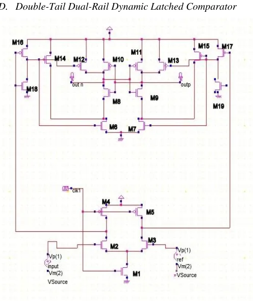
278 D. Double-Tail Dual-Rail Dynamic Latched Comparator
Figure V Double-Tail Dual-Rail Dynamic Latched Comparator
Operations: The diagram (Figure V) shows the schematic of the Double-Tail Dual-Rail Dynamic Comparator. This comparator eliminated the dual clock system which is very difficult to control for positive and negative. Due to synchronization is no needed between clock and clock B. Due to this, comparator shows lesser power dissipation than the all other comparators but it gives slower output then other comparators
IV. COMPARATIVE ANALYSIS
TABLEI
SUMMARY RESULT
Topology Parameters of comparator
No. of transistor
Power dissipation (µW) Pre amplifier based
comparator
20 102.5
Double Tail Latch Type Voltage Sense Amplifier
22 64.7
Dynamic comparator 23 19
Double tail dual rail comparator
27 10.2
This table is prepared after simulation of each comparator in HSPICE , by which power dissipation is calculated and output of comparators are analysed so as in table , Double Tail Dual Rail Comparator consumes less power as compare to all other comparators
V. CONCLUSION
This paper explains operation of different comparators and its design. It help designer to analyze different comparator. It give brief knowledge about the comparator. The comparative analysis of comparator on the basis of power consumed by comparator which has simulated in HSPICE. So we can conclude that double tail dual rail dynamic type comparator consumes lesser power than other comparator.
REFERENCES
[1] Phillip E. Allen ,Dougles R. Holberg “CMOS Analog Circuit Design” second edition OXFORD UNIVERSITY PRESS
[2] B. Razavi, “Principle of data conversion system design” IEEE PRESS
[3] Aalay Kapadia, Prof. Vijay Savani “Analysis And Characterization of Different Comparator Topologies”, International Journal of Scientific & Technology Research Volume 1, issue 11, December 2012
[4] Pedro M.Figueiredo, Joao C.Vital, “Kickback Noise Reduction Techniques for CMOS Latched Comparator”, IEEE Transactions on Circuits and Systems, vol.53, no.7, pp.541-545, July 2006. [5] B. Murmann et al., "Impact of scaling on analog performance and
associated modeling needs," IEEE Trans. Electron Devices, vol. 53, no. 9, pp. 2160-2167, Sep. 2006.
[6] Jun He, Sanyi Zhan, Degang Chen, and R.L. Geiger, “Analyses of Static and Dynamic Random Offset Voltages in Dynamic Comparators,” IEEE Trans. Circuits Syst. I: Reg. Papers, vol. 56, pp. 911-919, May 2009.
[7] M. Miyahara, Y. Asada, P. Daehwa and A. Matsuzawa, “A Low-Noise Self- Calibrating Dynamic Comparator for High-Speed ADCs,” in Proc. A-SSCC, pp. 269-272, Nov. 2008.
[8] Johns D., Martin K., Analog Integrated Circuit Design, Wiley India Pvt. Ltd., 2008
[9] Cadence Online Documentation. Avilable: http://www.cadence.com [10] Amin Nikoozadeh, Student Member, IEEE, and Boris Murmann, Member, IEEE” An Analysis of Latch Comparator Offset Due to Load Capacitor Mismatch” IEEE TRANSACTIONS ON CIRCUITS AND SYSTEMS—II: EXPRESS BRIEFS, VOL. 53, NO. 12, DECEMBER 20 Apisak Worapishet “Speed and Accuracy Enhancement Techniques for High-Performance Switched-Current Comparators” IEEE Journal of Solid-State Circuits, Vol. 36, No. 4, [11] Randall White”Analysis of Errors in a Comparator-Based
Switched-Capacitor Biquad Filter” IEEE Transactions on Circuits and Systems—Ii: Express Briefs, Vol. 56, No. 9, September 2009 [12] Bernhard Goll “A Comparator with Reduced Delay Time in 65-nm
[image:4.612.50.298.133.427.2] [image:4.612.63.276.556.711.2]International Journal of Emerging Technology and Advanced Engineering
Website: www.ijetae.com (ISSN 2250-2459,ISO 9001:2008 Certified Journal, Volume 5, Issue 11, November 2015)
279 [13] Jaeha Kim, Member, IEEE, Brian S. Leibowitz, Member, IEEE,
Jihong Ren, Member, IEEE, and
[14] Chris J. Madden, Member, IEE E” Simulation and Analysis of Random Decision Errors in Clocked Comparators” IEEE
TRANSACTIONS ON CIRCUITS AND SYSTEMS—I:
REGULAR PAPERS, VOL. 56, NO. 8, AUGUST 2009
[15] Todd Sepke, Member, IEEE, Peter Holloway, Charles G. Sodini, Fellow, IEEE, and Hae-Seung Lee, Fellow, IEEE “Noise Analysis for Comparator-Based Circuits” IEEE TRANSACTIONS ON CIRCUITS AND SYSTEMS—I: REGULAR PAPERS, VOL. 56, NO. 3, MARCH 2009
[16] John K. Fiorenza, Student Member, IEEE, Todd Sepke, Student Member, IEEE, Peter Holloway,
[17] Charles G. Sodini, Fellow, IEEE, and Hae-Seung Lee, Fellow, IEEE “Comparator-Based Switched-Capacitor Circuits for Scaled CMOS Technologies” IEEE JOURNAL OF SOLID-STATE CIRCUITS, VOL. 41, NO. 12, DECEMBER 2006
[18] Samaneh Babayan-Mashhadi, Student Member, IEEE, and Reza Lotfi, Member, IEEE” Analysis and Design of a Voltage Low-Power Double-Tail Comparator” IEEE TRANSACTIONS ON VERY LARGE SCALE INTEGRATION (VLSI) SYSTEMS, VOL. 22, NO. 2, FEBRUARY 2014
[19] Bernhard Goll, Member, IEEE, and Horst Zimmermann, Senior Member, IEEE” A Comparator With Reduced Delay Time in 65-nm CMOS for Supply Voltages Down to 0.65 V” IEEE
TRANSACTIONS ON CIRCUITS AND SYSTEMS—II:
EXPRESS BRIEFS, VOL. 56, NO. 11, NOVEMBER 2009 [20] Monica Rose Joy, 2Thangamani M. “ Design and Analysis of Low