Index
1
Introduction
2
Installation
3
Hardware User's Manual
4 Appendices to the
Hardware User's Manual
,
5 Copies of Data Sheets
6
Eagle Module
7
Introduction to VMEPROM
8
Appendices to the
VMEPROM Introduction
9
Bios Source Code Listing
10
User Notes
1 1
Options/ Applications/
SYS68K/CPU-40/41
USER'S MANUAL
Revision No.2
February 1992
FORCE COMPUTERS Inc./GmbH
All Rights Reserved
NOTE
The information in this document has been carefully checked and is believed to be
entirely reliable. FORCE COMPUTERS makes no warranty of any kind with regard to
the material in this document, and assumes no responsibility for any errors that may
appear in this document. FORCE COMPUTERS reserves the right to make changes
without notice to this, or any of its products, to improve reliability, performance or
design.
FORCE COMPUTERS assumes no responsibility for the use of any circuitry other than
circuitry which is part of a product of FORCE COMPUTERS GmbH/Inc.
FORCE COMPUTERS does not convey to the purchaser of the product described
herein any license under the patent rights of FORCE COMPUTERS GmbH/Inc. nor the
rights of others.
FORCE COMPUTERS Inc.
3165 Winchester Blvd.
Campbell, CA 95008-6557
U.S.A.
Phone: (408) 370-6300
FAX: (408) 374-1146
FORCE COMPUTERS FRANCE Sari
11, rue Casteja
92100 Boulogne
France
Phone: (1) 4620 37 37
Telex : 206 304 forc-f
FAX: (1) 4621 35 19
FORCE COMPUTERS GmbH
Prof.-Messerschmitt-Str. 1
0-8014 Neubiberg/Munich
West Germany
Phone: (089) 608 14-0
Telex: 524190 forc-d
FAX: (089) 609 77 93
FORCE Computers UK Ltd.
No. 1 Holly Court
3 Tring Road
Wendover
Buckinghamshire HP
England
Phone: (0296) 625456
Telex: 838033
1.
1 . 1
2.
2.1 2.2 2.2.1 2.2.2 2.2.3 2.2.4 2.3 2.4 2.5 2.6 2.7 2.8 2.8.1 2.8.2 2.9 2.10 2.10.1 2.11 2.12 2.13 2.143.
4.5.
TABLE OF CONTENTS
GENERAL INFORMATION . . . .
Features of the CPU Board . . . .
THE PROCESSOR . . . • . . .
The CPU 68040 . . . .
The Shared RAM . . . . The DRM-O 1/4 . . . . The DRM-O 1/1 6 . . . . The SRM-01/4 . . . . The SRM-01/8 . . . .
The System EPROM . . . .
The Local SRAM . . . .
The Local FLASH EPROM . . . .
The Boot EPROM . . . .
The FGA-002 . . . .
The PI/T 68230 . . . . The I/O Configuration of PI/T 1 . . . . The I/O Configuration of PIIT2 . . . .
The Real Time Clock 72423 . . . .
The DUSCC 68562 . . . . The I/O Configuration of DUSCC 1 and DUSCC2 . . . .
The EAGLE Modules . . . .
The VMEbus Interface . . . .
The Monitor of the CPU board . . . .
Default Jumper Settings on the CPU Board . . . .
SPECIFICATIONS OF THE CPU BOARD . . . .
ORDERING INFORMATION . . . .
Figure 1-1: Figure 1-2: Figure 2-1: Figure 2-2:
LIST OF FIGURES
Photo of the CPU Board . . . . Block Diagram of the CPU Board . . . . Location Diagram for All Jumperfields . . . . The Front Panel of the CPU Board . . . .
LIST OF TABLES
1-2 1-3 2-20 2-21
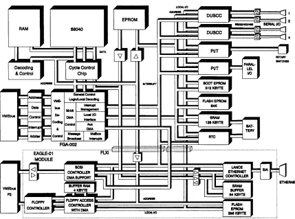
Table 1-1: The Memory Map . . . . . . .. 1-6 Table 1-2: The Base Addresses of the Local liD Devices . . . .. 1-7
SECTION 1 INTRODUCTION
1. GENERAL INFORMATION
This CPU board is a high performance single board computer based on the 68040 microprocessor and the VMEbus. The board incorporates a modular I/O subsystem which provides a high degree of flexibility for a wide variety of applications. The CPU board can be used with or without an I/O subsystem, called an "EAGLE" module.
The board is able to hold a RAM Module which can be DRAM (CPU-40) or SRAM (CPU-41) based.
The CPU-40/41 family design utilizes all of the features of the powerful FORCE Gate Array (FGA-002). Among its features is a 32-bit DMA controller which supports local (shared) memory, VMEbus and I/O data transfers for maximum performance, parallel real time operation and responsiveness.
The EAGLE modules are installed on the CPU board via the FLXi (FORCE Local eXpansion interface). This provides a full 32-bit interface between the base board and the EAGLE module I/O subsystem, providing a range of I/O options.
Four multi protocol serial I/O channels, a parallel I/O channel and a Real Time Clock with on-board battery backup are installed on the base board which, in combination with EAGLE modules, make the CPU board a true single board computer system.
A broad range of operating systems and kernels is available for the CPU board. However, as with all FORCE COMPUTERS' CPU cards, VMEPROM firmware is provided with the board at no extra cost. VMEPROM is a Real Time Kernel and is installed on the CPU board in the two 16-bit wide EPROM sockets, which results in a 32-bit wide System EPROM area. This ensures that the board is supplied ready to use.
SYS68K/CPU-40/41 USER'S MANUAL
Figure 1 -1: Photo of the CPU Board
;-2
FORCE COMPUTERS
o
[image:12.615.82.465.164.670.2]SECTION 1 INTRODUCTION
Figure 1-2: Block Diagram of the CPU Board
[image:13.612.145.574.267.586.2]SYS68K/CPU-40/41 USER'S MANUAL FORCE COMPUTERS
1 . 1 Features of the CPU Board
•
68040 microprocessor: 25.0 MHz on CPU-40B/41 B/x•
68040 microprocessor: 33.0 MHz on CPU-40D/41 D/x•
Shared DRAM Module: 4 Mbyte DRAM with Burst Read/Write and Parity Generation and Checking (DRM-O 1/4)•
Shared SRAM Module:16 Mbyte DRAM with Burst Read/Write and Parity Generation and Checking (DRivi-O iii 6j
4 Mbyte SRAM with Burst Read/Write (SRM-01 /4)
8 Mbyte SRAM with Burst Read/Write (SRM-01 /8)
• 32-bit high speed DMA controller for data transfers to/from the shared RAM, VMEbus memory and EAGLE modules; DMA controller is installed in the FGA-002.
• Two system EPROM devices supporting 40-pin devices. Access from the 68040 using a 32-bit data path
• One boot EPROM for local booting, initialization of the I/O chips and configuration of the FGA-002
• 1 28 Kbyte SRAM with on-board battery backup
• 1 28 Kbyte FLASH EPROM
• FLXi interface for installation of one EAGLE module
• Four Serial I/O interfaces, configurable as RS232/RS422/RS485, available on the front panel
• 8-bit parallel interface with 4-bit handshake
• Two 24-bit timers with 5-bit prescaler
• One 8-bit timer
• Real Time Clock with calendar and on-board battery backup
• Full 32-bit VMEbus master/slave interface, supporting the following data transfer types:
• A32, A24, A 16 : 08, 016, D32 - Master • A32, A24: 08,016,032 - Slave
• UAT. RMW, ADO
1 I!
SECTION 1 INTRODUCTION
Features of the CPU Board (cont'd)
• Four-level VMEbus arbiter
• SYSCLK driver
• VMEbus interrupter OR 1-7)
• VMEbus interrupt handler (lH 1-7)
• Support for ACFAIL
*
and SYSFAIL• Bus timeout counters for local and VMEbus access (1 5 psec)
• VMEPROM, Real Time Multitasking Kernel with monitor, file manager and debugger
SYS68K/CPU-40/41 USER'S MANUAL FORCE COMPUTERS
The following table summarizes the memory map of the CPU board.
Table 1-1 : The Memory Map
I
Start EndAddress Address Type
00000000 003FFFFF Shared Memory (4 Mbyte)
00000000 007FFFFF Shared Memory (8 Mbyte) or I
00000000 OOFFFFFF Shared Memory (1 6 Mbyte)
I
III
00400000 F9FFFFFF VMEbus Addresses (4 Mbyte Shared Memory) A~~. n~~ ~~A ~~~ ~n IMv~. Uv~, U~~,UIO, uo
00800000 F9FFFFFF VMEbus Addresses (8 Mbyte Shared Memory)
I
A32: 032, 024, 016, 08
01000000 F9FFFFFF VMEbus Addresses (16 Mbyte Shared Memory)
I
A32: 032, 024, 016, 08I
FAOOOOOO FAFFFFFF Message Broadcast AreaFBOOOOOO FBFEFFFF VMEbus
A24: 032,024,016,08
FBFFOOOO FBFFFFFF VMEbus
A16: 032, 024,016, 08
FCOOOOOO
I
FCFEFFFF VMEbusA24: 016, 08
FCFFOOOO FCFFFFFF VMEbus
A16: 016,08
FOOOOOOO FEFFFFFF Reserved
FFOOOOOO FF7FFFFF SYSTEM EPROM
FF800000 FFBFFFFF Local I/O
FFCOOOOO FFC7FFFF LOCAL SRAM
FFC80000 FFCFFFFF Local FLASH EPROM
FFOOOOOO FFOFFFFF Registers of FGA-002
FFEOOOOO FFEFFFFF BOOT EPROM
FF803EOO FF803FFF VMEbus Arbiter
FFFOOOOO FFFFFFFF Reserved
[image:16.617.27.495.128.611.2]SECTION 1 INTRODUCTION
This table gives a brief overview of the local I/O devices and the equivalent base address.
Table 1-2: The Base Addresses of the
Local
110
Devices
BASE ADDRESS DEVICE
$FF803000
RTC
72423
$FF802000
DUSCC1
68562
$FF802200
DUSCC2
68562
$FF800COO
PIIT1
68230
$FF800EOO
PIIT2
68230
SECTION 1 INTRODUCTION
2. THE PROCESSOR
2.1 The CPU 68040
The 68040 is a third generation full 32 bit enhanced microprocessor. The 68040 is upward object code compatible with the 68030, 68020, 68010 and 68000 line of microprocessors.
The 68040 combines a central processing unit core, an instruction cache, a data cache, a memory management unit, and an enhanced bus controller.
This virtual memory processor utilizes multiple, concurrent execution units and a highly integrated architecture providing a high level of performance.
The 68040 processor combines a 68030 compatible integer unit, a 68881/68882 compatible floating point unit (FPU), memory management units (MMUs), and a 4 Kbyte instruction and data cache. Cache functionality is strengthened by the built-in on-chip bus snooping logic which instantly supports cache logic during multimaster applications.
Instruction administration is routed through both the integer unit and FPU, which link to the fully independent data and instruction memory units. Each memory unit consists of an MMU I an address
translation cache (ATC)' a main cache, and a snoop controller.
The internal blocks are designed to operate in parallel, allowing instruction execution to be overlapped. In addition, the internal caches, the on-chip memory management unit, and the enhanced bus controller operate parallel to one another.
The 68040 contains an enhanced bus controller that supports both synchronous/ asynchronous bus cycles and burst data transfers. It contains a nonmultiplexed address bus and data bus and supports 32 bits of address and data.
SYS68K/CPU-40/41 USER'S MANUAL FORCE COMPUTERS
Features of the 68040
• Nonmultiplexed 32 bit address and data buses
• 1 6 general purpose address and data registers (32 bit wide)
• 8 floating point data registers (80 bit wide)
• Two supervisor stack pointers (32 bit wide)
• 19 special purpose control registers
• 4 Kbyte instruction and 4 Kbyte data cache
• On-chip paged memory management unit
• Pipelined architecture with parallelism allowing accesses to internal caches, bus transfers, and instruction execution in parallel
• Synchronous bus cycles and burst read and write data transfers
• Complete floating point support given to the 68882 FPCP subset and software emulation
• 68030 compatible
• Low latency bus accesses to reduce cache miss penalty
• Maximized throughput from the integer unit, FPU, MMU and bus controller
SECTION 1 INTRODUCTION
2.2 The Shared RAM
On this CPU board the shared RAM is placed on a module to allow the adaption of DRAM or SRAM to the base board.
All signals which are needed to control the shared RAM are available on the RAM module connector. Therefore RAM devices with different access times can also be used on this CPU board to take advantage of the 68040 with higher frequency if it becomes available.
2.2.1 The DRM-01/4
The DRM-O 1/4 is a 4 Mbyte RAM module which is used on the CPU-40B/4.
Features of the DRM-O 1/4
• 4 Mbyte DRAM
• Burst READ and Burst WRITE capability
• Parity Generation and Checking
• Asynchronous refresh is provided every 14J.ls
• Accessible via VMEbus
The access address for the 68040 is $00000000 to $003FFFFF.
The access address for the VMEbus is programmable in 4 Kbyte steps through the FGA-002. The defined memory range can be write protected in coordination with the address modifier codes. For example, in supervisor mode the memory can be read and written, in user mode memory can only be read.
The DRAM module includes byte parity check for local and VMEbus accesses. If a parity error is detected on a VMEbus cycle, a BERR is forced to the VMEbus informing the requestor that a parity error has occurred. On local accesses, a Transfer Error Acknowledge (TEA) is forced to the processor if a parity error was detected.
The following chart lists the required CPU clock cycles and wait states for accessing the shared RAM.
Board 68040 Clock No. of CPU Clock No. of CPU Clock No. of Wait No. of Wait Type Frequency Cycles Counted Cycles for States for States for
From TS to TA Burst Cycles Normal Cycles Burst Cycles for Normal Cycles
CPU-40/8 25 MHz 4 1 3 0
SYS68K/CPU-40/41 USER'S MANUAL FORCE COMPUTERS
2.2.2 The DRM-01/16
The DRM-01/16 is a 16 Mbyte RAM module which is used on the CPU-40B/16.
Features of the DRM-O
1/16
• 1 6 Mbyte DRAM
• Burst READ and Burst WRITE capability
• Parity Generation and Checking
• Asynchronous refresh is provided every 1 4ps
• Accessible via VMEbus
The access address for the 68040 is $00000000 to $OOFFFFFF.
The access address for the VMEbus is programmable in 4 Kbyte steps through the FGA-002. The defined memory range can be write protected in coordination with the address modifier codes. For example, in supervisor mode the memory can be read and written, in user mode memory can only be read.
The DRAM module includes byte parity check for local and VMEbus accesses. If a parity error is detected on a VMEbus cycle, a BERR is forced to the VMEbus informing the requestor that a parity error has occurred. On local accesses, a Transfer Error Acknowledge (TEA) is forced to the processor if a parity error was detected.
The following chart lists the required CPU clock cycles and wait states for accessing the shared RAM.
Board 68040-B Clock No. of CPU Clock No. of CPU Clock No. of Wait No. of Wait Type Frequency Cycles Counted Cycles for States for States for
From TS to TA Burst Cycles Normal Cycles Burst Cycles for Normal Cycles
CPU-40/B 25 MHz 4 1 3 0
SECTION 1 INTRODUCTION
2.2.3 The SRM-01/4
The SRM-O 1/4 is a 4 Mbyte RAM module which is used on the CPU-41 B/4.
Features of the SRM-O 1/4
• 4 Mbyte SRAM
• Burst READ and Burst WRITE capability
• Battery Backup via VMEbus
• Accessible via VMEbus
The access address for the 68040 is $00000000 to $003FFFFF.
The access address for the VMEbus is programmable in 4 Kbyte steps through the FGA-002. The defined memory range can be write protected in coordination with the address modifier codes. For example, in supervisor mode the memory can be read and written, in user mode memory can only be read.
Parity check is not necessary for SRAM devices, because these components are protected against soft errors owing alpha emission. The following chart lists the required CPU clock cycles and wait states for accessing the shared RAM.
Board 68040 Clock No. of CPU Clock No. of CPU Clock No. of Wait No. of Wait Type Frequency Cycles Counted Cycles for States for States for
From TS to TA Burst Cycles Normal Cycles Burst Cycles for Normal Cycles
CPU-41!S 25 MHz 3 1 2 0
SYS68K/CPU-40/41 USER'S MANUAL FORCE COMPUTERS
2.2.4 The SRM-01/8
The SRM-01 /8 is an 8 Mbyte RAM module which is used on the CPU-41 B/8.
Features of the SRM-01 /8
• 8 Mbyte SRAM
• Burst READ and Burst WRITE capability
• Battery Backup via VMEbus
• Accessible via VMEbus
The access address for the 68040 is $00000000 to $007FFFFF.
The access address for the VMEbus is programmable in 4 Kbyte steps through the FGA-002. The defined memory range can be write protected in coordination with the address modifier codes.
For example, in supervisor mode the memory can be read and written, in user mode memory can only be read.
Parity check is not necessary for SRAM devices, because these components are protected against soft errors owing alpha emission. The following chart lists the required CPU clock cycles and wait states for accessing the shared RAM.
Board 68040 Clock No. of CPU Clock No. of CPU Clock No. of Wait No. of Wait Type Frequency Cycles Counted Cycles for States for States for
From TS to TA Burst Cycles Normal Cycles Burst Cycles for Normal Cycles
CPU-41/B 25 MHz 3 1 2 0
SECTION 1 INTRODUCTION
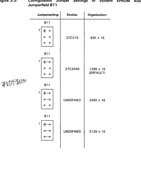
2.3 The System EPROM
The CPU board offers two 40-pin EPROM sockets for the installation of two 16-bit wide EPROM devices. The EPROMs present a full 32-bit data path to the processor enabling maximum performance. The following devices are supported in the system EPROM area:
Supported Device Types in the System EPROM Area:
Organization Total Memory Capacity
64K x 16 256 Kbytes
128Kx16 512 Kbytes
256K x 16 1 Mbyte
512K x 16 2 Mbytes
2.4 The Local SRAM
The CPU board contains a 1 28K
*
8 bit SRAM. Battery backup is provided via the on-board battery or the VMEbus+
5VSTDBY line.2.5 The Local FLASH EPROM
A 128 Kbyte FLASH EPROM is included on the base board of the CPU-40 which can be used as additional data backup under conditions of power down for long periods. FLASH EPROM is ideal to hold details of the board status, such as software revision or user data which is to be kept permanently.
2.6 The Boot EPROM
The CPU board contains, in addition to the two system EPROMs, a single boot EPROM to boot the local microprocessor, initialize all I/O devices and program the board-dependent functions of the FGA-002. All basic initialization of the I/O devices and the FGA-002 are made through the boot EPROM.
In addition, the boot EPROM contains user utility routines, which may be called out of the user's application program. These routines provide easy software access to the functionality of the FGA-002 (DMA controller, FORCE Message Broadcast, Interrupt Management, etc.).
SYS68K/CPU-40/41 USER'S MANUAL FORCE COMPUTERS
2.7 The FGA-002
One of the main features on this CPU board is the FGA-002 Gate Array with 24,000 gates and 281 pins. The FGA-002 controls the local bus and builds the VMEbus interface. It also ipcludes a DMA controller, a complete interrupt handler, message broadcast interface (FMB), timer functions, mailbox locations, and a VMEbus interrupter. This gate array monitors the local bus, which in turn signifies that if any local I/O device is to be accessed, the gate array overrules all control signals, used address signals, and data signals.
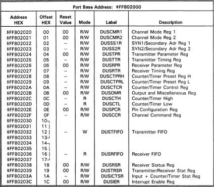
The FGA-002 serves as a VMEbus manager. All VMEbus address and data lines are connected to the gate array through the buffers. Additional functions such as the VMEbus interrupt handler are also installed on the FGA-002. The on-chip Drv1A controiler can access the iocai memory, VMEbus memory, and on-board devices which are able to function in a DMA mode. The start address of the FGA-002 registers is $FFDOOOOO. All registers of the gate array and associated functions are described in detail in the FGA-002 Users Manual. On the following page you will find a list of features for the FGA-002.
Features of the FGA-002
• 32 bit DMA Controller
• 2 Message Broadcast Channels (FMB)
• 8 Mailbox Interrupt Channels
• One 8 bit timer
• Complete Interrupt Management for VMEbus interrupts, ACFAIL, SYSFAIL, Onboard Interrupts and FGA-002 internal interrupts
• VMEbus interface including a single level arbiter
• Decoding logic for accesses to the Shared Memory of the CPU board
A complete functional description of the FGA-002 may be found in the FGA-002 Users Manual.
SECTION 1 INTRODUCTION
2.8 The PIIT 68230
The MC68230 ParallellnterfacetTimer (PItT) provides versatile double buffered parallel interfaces and an operating system oriented timer for MC68000 systems. The parallel interfaces operate in unidirectional or bidirectional modes, 8 or 16 bits wide. The PItT timer contains a 24 bit wide counter and a 5 bit prescaler.
• MC68000 Bus Compatible
•
Port Modes Include:Features of the PIIT
Bit I/O
Unidirectional 8 bit and 1 6 bit Bidirectional 8 bit and 16 bit
• Selectable Handshaking Options
• 24 bit Programmable Timer
• Software Programmable Timer Modes
• Contains Interrupt Vector Generation Logic
• Separate Port and Timer Interrupt Service Requests
• Registers are ReadIWrite and Directly Addressable
SYS68K/CPU-40/41 USER'S MANUAL FORCE COMPUTERS
2.8.1 The
1/0
Configuration of PltT1
Port A is connected to the two 4 bit HEX rotary switches provided on the front panel for application dependent settings.
Port B is used for programming the local base address for A24 accesses from the VMEbus.
Port C is used for port and timer interrupts and to control the RMC behavior of the board.
2.8.2 The
1/0'
Configuration of PltT2
Port A and the handshake lines are routed to a 24-pin header which allows the connection of a flat cable. 8 bits are connected to port A of the PI/T and can be used as inputs or outputs, with the remaining 4 bits being connected to the handshake pins of the PI/T. This port can be used to establish a "Centronics type" interface.
Port B allows the memory capacity of the Shared RAM to be read. Each CPU board of this type contains three readable status bits describing the memory capacity. In addition, the CPU board type can be read through the remaining 5 bits.
Port C grants the RAM type (DRAM/SRAM) burst and parity capability of the Shared RAM to be read.
A "Powerup Reset" can be initiated by software.
SECTION 1 INTRODUCTION
2.9 The Real Time Clock 72423
There is a Real Time Clock (RTC) 72423 installed on the CPU board. The CPU board contains a self supportive battery to sustain the RTC during power down.
Features of the RTC
• Built-in quartz oscillator makes regulation unnecessary and allows easy design
• Direct bus compatibility (120 ns access time)
• Incorporated built-in time (hour, minute, second), and date (year, month, week, day) counters
• 12 hour and 24 hour clock switchover functions and automatic leap year setting
• Interrupt masking
• An error adjustment time function of 30 seconds
• READ, WRITE, HOLD, STOP, RESET, and CHIP SELECT inputs
• The C-MOS IC boasts low current consumption and features a backup function
• A 24-pin so package
SYS68K/CPU-40/41 USER'S MANUAL FORCE COMPUTERS
2.10 The DUSCC 68562
The Dual Universal Serial Communications Controller (DUSCC) 68562 is installed to communicate with terminals, computers, or other equipment.
The DUSCC is a single chip MOS-LSI communications device providing two independent, multi protocol, full duplex receiver/transmitter channels in a single package. Each channel consists of a receiver, transmitter, 16-bit multifunction counter/timer, digital phaselocked loop (DPLL)' parity/CRC generator and checker, and associated control circuits.
Features of the DUSCC
• Dual full duplex synchronous/asynchronous receiver and transmitter
• Multiprotocol operation consisting of:
BOP: COP:
HDLC/ADCCP, SDLC, SDLC Loop, X.25 or X.75 link level BISYNC, DDCMP, X.21
ASYNC: 5-8 bit plus optional parity
• Programmable data encoding formats: NRZ, NRZI, FMO, FM1, Manchester
• 4 character receiver and transmitter FIFOs
• Individual programmable baud rate for each receiver and transmitter
• Digital phase locked loop
• User programmable counter/timer
• Programmable channel modes full/half duplex, auto echo, local loopback
• Modem control signals for each channel: RTS, CTS, DCD
• CTS and DCD programmable autoenables for Receiver (RX) and Transmitter (TX)
• Programmable interrupt on change of CTS or DCD
SECTION 1 INTRODUCTION
2.10.1 The I/O Configuration of DUSCC1 and DUSCC2
The four channels may be configured to function as a RS232 or RS422/RS485 compatible interface. Termination resistors can be installed to adapt various cable lengths and reduce reflections upon the selection of the RS422/RS485 compatible interface. The DUSCC can interrupt the local CPU at a specified programmable IRQ level.
I/O Signals for DUSCC1:
The I/O signal assignment of channel 1 to 2 is listed as follows:
Signal Input Output 9 Pin Micro Description D-Sub Connector
DCD X 1 Data Carrier Detect
RXD X 2 Receive Data
TXD X 3 Transmit Data
DTR X 4 Data Terminal Ready
GND 5 Signal GND
DSR X X
6
Data Set ReadyRTS X 7 Request to Send
CTS X 8 Clear to Send
GND
9
Signal GNDSYS68K/CPU-40/41 USER'S MANUAL FORCE COMPUTERS
The I/O signals of channel 1 can be connected to the VME connector P2 in parallel to the 9-pin Micro D-Sub connector as follows:
Signal Input Output VME Connector Description P2
DCD X c29 Data Carrier Detect
RXD X c30 Receive Data
TXD X c31 Transmit Data
f""I,O v ,.,,')') F""'\",+", T""'r'Y"'!I.:~",1 0"",,..1 ...
LJ I 11
"
vv4- LJO lO I vi 11111 101 I lC;OU YDSR X X a29 Data Set Ready
RTS X a30 Request to Send
CTS X a31 Clear to Send
GND a32 Signal GND
NOTE
This is only possible if these VMEbus P2 lines are not used by an EAGLE module.
1/0 Signals for DUSCC2:
The I/O signal assignment of channels 3 and 4 is listed as follows:
Signal Input Output 9 Pin Micro Description D-Sub Connector
DCD X 1 Data Carrier Detect
RXD X 2 Receive Data
TXD X 3 Transmit Data
DTR X 4 Data Terminal Ready
GND 5 Signal GND
DSR X X 6 Data Set Ready
RTS X 7 Request to Send
CTS X 8 Clear to Send
GND 9 Signal GND
SECTION 1 INTRODUCTION
2.11 The EAGLE Modules
EAGLE modules are 1/0 subsystems designed not only to increase the functionality of the board but to add the exact 1/0 features to fit the application requirement. EAGLE modules connect directly onto the FLXi of the base board. FLXi and EAGLE modules will be a feature on future FORCE board generations to ensure continued flexibility.
If your CPU board is assembled with an EAGLE module please refer to the "EAGLE Module" manual which is shipped with this board and should be placed in Section 6 of this manual.
2.12 The VMEbus Interface
The CPU board has a full 32-bit VMEbus interface. The address modifier codes for A 16, A24 and A32 addressing are fully supported in master mode. In slave mode, the address modifiers for A32 and A24 are fully supported.
Read-Modify-Write cycles are fully supported to allow multiple CPU boards to be synchronized via the shared RAM. The FGA-002 determines whether or not an access to the shared RAM is allowed and, if allowed, controls the access cycle.
The CPU board provides an interrupt handler capability (I H 1-7) which can be enabled/disabled by programming the FGA-002. The CPU board also provides an interrupter function which enables the board to send interrupts to the VMEbus on seven programmable levels with a software-programmable vector.
The following bus release modes are supported:
RWD
=
Release When Done ROR=
Release On Request RBCLR=
Release On Bus Clear RAT=
Release After Timeout REC=
Release Every Cycle ROACF=
Release On ACFAIL*
SYS68K/CPU-40/41 USER'S MANUAL FORCE COMPUTERS
Each of the listed modes is software programmable inside the gate array. The bus request level of the CPU board is jumper or software selectable (BRO-3).
The DMA controller installed in the FGA-002 on the CPU board is able to access the VMEbus interface independently from the microprocessor, enabling VMEbus communication to take place without impacting the processing capabilities of the rest of the board for number crunching or servicing on-board I/O.
A four level arbiter with round robin and prioritized round robin arbitration modes, a power monitor, a SYSRESET* generator, IACK* daisy chain driver and support for ACFAIL *, SYSFAIL
*
and SYSCLK complete the VMEbus interface."
..
,..SECTION 1 INTRODUCTION
2.13 The Monitor of the CPU board
Every CPU board contains VMEPROM, a real time multitasking monitor debugger. It consists of a powerful real time kernel, file manager and monitor/debugger with 68040 line assembler/disassembler.
The monitor/debugger includes all functions to control the real time kernel and file manager as well as all tools required for program debugging such as breakpoints, tracing, memory display, memory modify and host communication.
VMEPROM supports several memory and I/O boards on the VMEbus to take full advantage of the file manager and kernel functions.
A built-in selftest checks all on-board devices and memory. This allows detection of any failures on the board.
Memory initialization and test commands offer easy installation of global memory in the environment on the local RAM and/or the VMEbus.
The one line assembler/disassembler is 68040 compatible and supports all 68040 commands in the original mnemonic described in the MC 68040 User's Manual.
SYS68K/CPU-40/41 USER'S MANUAL FORCE COMPUTERS
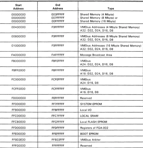
2.14 Default Jumper Settings on the CPU Board
The following are the default jumper settings and a location diagram displaying all jumpers. Default Jumper Settings for the CPU
Jumperfield Description Default Schematics
Connection
B2 Reset Voltage Sensor
---
SH4B4
B20 Backup Supply for Local SRAM and
---
SH4RTC via + 5 VSTDBY B2
B1 Backup Supply for Local SRAM and 1-2 SH4
RTC via Bat 1 B2
Default Jumper Settings for System EPROMs and SRAM/EEPROM
Jumperfield Description Default Schematics
Connection
B11 System EPROM device select 1-6 SH5
A4
B16 FLASH EPROM write dis-tenable 1-2 SH4 C2
Default Jumper Settings for Serial 1/0 (RS232)
Jumperfield Description Default Schematics
Connection
B3 Connector 1, PD 1 2-15 SH6
(DUSCC 1 Port # 1 ) 8-9 B2
B4 Connector 2, PD2 2-15 SH6
(DUSCC1 Port #2) 8-9 B3
B5 Connector 1, PD 1 --- SH6
(DUSCC1 Port #1) C2
B6 Connector 2, PD2 --- SH6
(DUSCC Port #2) C3
B7 Connector 3, PD3 2-15 SH7
(DUSCC2 Port #3) 8-9 B2
B8 Connector 4, PD4 2-15 SH7
(DUSCC2 Port #4) 8-9 B3
B9 Connector 3, PD3
---
SH7(DUSCC2 Port #3), PD3 C2
B10 Connector 4, PD4 --- SH7
(DUSCC Port #4), PD4 C3
SECTION 1 INTRODUCTION
Default Jumper Settings for VMEbus
Jumperfield Description Default Schematics
Connection
819 Four level Arbiter Request Level 1-6 SH9
2-5 84
3-4
813 SYSCLK 1-8 SH10
SYSFAIL 2-7 C2
Receive VMEbus RESET 3-6 Drive VMEbus RESET 4-5
Default Jumper Settings for Test
Jumperfield Description Default Schematics
Connection
817 Clock Signal to CPU 1-2 SH16
A1
Headers for 12 Bit 1/0 and 8 Bit 1/0
Jumperfield Description Default Schematics
Connection
812 User I/O
---
SH8D1
SYS68K/CPU-40/41 USER'S MANUAL
Figure 2- 1 : Location Diagram for All Jumperfields
o
D
D
D
o
~DJI9
J::fi
D
D~
D~
2-20
FORCE COMPUTERS
[image:38.615.64.457.127.687.2]SECTION 1
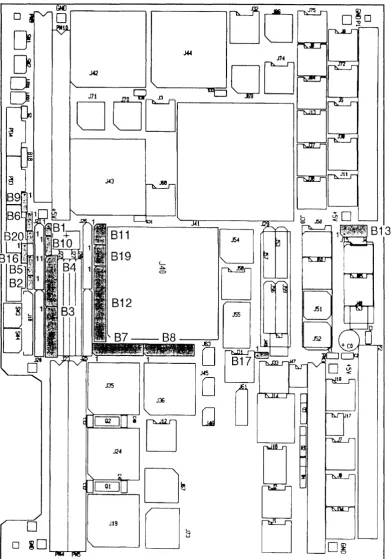
Figure 2-2: The Front Panel of the ·CPU Board
~1
!RESET
,
ABORTe
RUNG8M
@4
o@3
o@2
o@1
o EAGLE MODULE DEPENDENT FORCEo
2-21 INTRODUCTIONEJ
3 4 5 6
1 7
o ___
8F 9
E A
DeB
EJ
3 4 5 6
1 7
o ___
8F 9
E A
[image:39.615.110.515.125.725.2]SYS68K/CPU-40/41 USER'S MANUAL FORCE COMPUTERS
This page intentionally left blank
SECTION 1 INTRODUCTION
3. SPECIFICATIONS OF THE CPU BOARD
CPU Type 68040
CPU Clock Frequency CPU-40B/x 25.0 MHz CPU-400/x 33.0 MHz
Shared DRAM Capacity with Parity CPU-40X/4 4 Mbytes CPU-40X/16 16 Mbytes
Shared SRAM Capacity CPU-41 X/4 4 Mbytes CPU-41 X/8 8 Mbytes
SRAM Capacity with On-board Battery Backup 128 Kbytes
FLASH EPROM 128 Kbytes
Number of System EPROM Sockets 2
Data Path 32-Bits
Serial I/O Interfaces (68562) 4
RS232/RS422/RS485 Compatible 4 of 4
24-bit Timer with 5-bit Prescaler 2
8-bit Timer 1
Parallel I/O Interface (68230) 12 Lines
Real Time Clock with On-board Battery Backup 72423
VMEbus Interface A32, A24, A 16:08, 016, 032, UAT, RMW Master A32, A24:08, 016, 032, RMW Slave
Four Level Arbiter Yes
SYSCLK Driver Yes
Mailbox Interrupts 8
FORCE Message Broadcast FMB FIFO 0 8 Bytes FMB FIFO 1 1 Byte
VMEbus InterrupterNMEbus and Local Interrupt Handler 1 to 7 All Sources can be Routed to a Software Programmable IRQ Level Yes
RESET/ABORT Switch Yes
VMEPROM Firmware Installed on All Board Versions 256 Kbytes
Power Requirements +5V minImax 5.2A/6.0A
+ 12V minimax 0.1A/0.3A -12V min/max 0.1A/0.3A
Operating Temperature with Forced Air Cooling 0 to + 50°C
Storage Temperature -40 to + 85°C
Relative Humidity (noncondensing) 0 to 95%
Board Dimensions 234x160mm/9.2x6.3in
No. of Slots Used 1
SYS68K/CPU-40/41 USER'S MANUAL FORCE COMPUTERS
This page intentionally left blank
SECTION 1 INTRODUCTION
4. ORDERING INFORMATION
SYS6SK/CPU-40B/4-00 SYS6SK/CPU-40B/4-0 1 SYS6SK/CPU-40B/1 6-00 SYS6SK/CPU-40B/16-01 SYS6SK/CPU-400/4-00 SYS6SK/CPU-400/4-0 1 SYS6SK/CPU-400/16-00 SYS6SK/CPU-400/16-01 SYS6SK/CPU-41 B/4-00 SYS6SK/CPU-418/4-01 SYS6SK/CPU-41 B/S-OO SYS6SK/CPU-41 B/S-01 SYS6SK/CPU-41 0/4-00 SYS6SK/CPU-41 0/4-01 SYS6SK/CPU-410/S-00
25.0 MHz 68040 based CPU board with DMA, 4 Mbyte shared DRAM, 4 serial
1/0 channels, FLXi, VMEPROM. Documentation included.
25.0 MHz 68040 based CPU board with DMA, 4 Mbyte shared DRAM, 4 serial
1/0 channels, EAGLE-01 C (SCSI, floppy disk and Ethernet Interface),
VMEPROM. Documentation included.
25.0 MHz 68040 based CPU board with DMA, 16 Mbyte shared DRAM, 4 serial
110 channels, FLXi, VMEPROM. Documentation included.
25.0 MHz 68040 based CPU board with DMA, 16 Mbyte shared DRAM, 4 serial
110 channels, EAGLE-01 C (SCSI, floppy disk and Ethernet Interface),
VMEPROM. Documentation included.
33.0 MHz 68040 based CPU board with DMA, 4 Mbyte shared DRAM, 4 serial
110 channels, FLXi, VMEPROM. Documentation included.
33.0 MHz 68040 based CPU board with DMA, 4 Mbyte shared DRAM, 4 serial
110 channels, EAGLE-O 1 C (SCSI, floppy disk and Ethernet Interface),
VMEPROM. Documentation included.
33.0 MHz 68040 based CPU board with DMA, 16 Mbyte shared DRAM, 4 serial
liD channels, FLXi, VMEPROM. Documentation included.
33.0 MHz 68040 based CPU board with DMA, 16 Mbyte shared DRAM, 4 serial
liD channels, EAGLE-01 C (SCSI, floppy disk and Ethernet Interface),
VMEPROM. Documentation included.
25.0 MHz 68040 based CPU board with DMA, 4 Mbyte shared SRAM, 4 serial
liD channels, FLXi, VMEPROM. Documentation included.
25.0 MHz 68040 based CPU board with DMA, 4 Mbyte shared SRAM, 4 serial
liD channels, EAGLE-01 C (SCSI, floppy disk and Ethernet Interface),
VMEPROM. Documentation included.
25.0 MHz 68040 based CPU board with DMA, 8 Mbyte shared SRAM, 4 serial I/O channels, FLXi, VMEPROM. Documentation included.
25.0 MHz 68040 based CPU board with DMA, 8 Mbyte shared SRAM, 4 serial
110 channels, EAGLE-01 C (SCSI, floppy disk and Ethernet Interface),
VMEPROM. Documentation included.
33.0 MHz 68040 based CPU board with DMA, 4 Mbyte shared SRAM, 4 serial I/O channels, FLXi, VMEPROM. Documentation included.
33.0 MHz 68040 based CPU board with DMA, 4 Mbyte shared SRAM, 4 serial
liD channels, EAGLE-O 1 C (SCSI, floppy disk and Ethernet Interface),
VMEPROM. Documentation included.
33.0 MHz 68040 based CPU board with DMA, 8 Mbyte shared SRAM, 4 serial I/O channels, FLXi, VMEPROM. Documentation included.
SYS68K/CPU-40/41 USER'S MANUAL FORCE COMPUTERS
SYS6SK/CPU-410/S-01
SYS6SKIIOBP-1
SYS6SK/CABLE MICRO-9 SET 1
SYS6SK/CABLE MICRO-9 SET 2
SYS68KNMEPROM/40/U P
SYS6SKNMEPROM/UM
SYS6SK/CPU-40/UM
SYS6SK/FGA-002/UM
33.0 MHz 68040 based CPU board with DMA, 8 Mbyte shared SRAM, 4 serial I/O channels, EAGLE-01 C (SCSI, floppy disk and Ethernet Interface), VMEPROM. Documentation included.
Backpanel for single board computers providing SCSI and floppy disk drive connectors.
Set of three adapter cables 9-pin micro D-Sub male connector to 9-pin O-Sub female connector, length 2 m.
Set of four adapter cables 9-pin micro O-Sub male connector to 25-pin O-Sub female connector, length 2 m.
VMEPROM update service for the SYS68K/CPU-40 series.
VMEPROM User's Manual excluding the SYS68K/CPU-40 description.
User's Manual for the SYS68K/CPU-40 product, including VMEPROM User's Manual and EAGLE-01 C User's Manual (separately available as EAGLE-01 C/UM).
User's Manual for the FGA-002 Gate Array.
SECTION 3 HARDWARE USER'S MANUAL
6.8 RESET Generation
There is an IEEE 1014 compatible SYSRESET* driver installed on the
epu
board. The RESET generator circuitry is operable if the power supplyvee
is at least 3 volts. The RESET signal can be asserted (low) on anyone of the following conditions:• Front Panel RESET switch toggled
• Voltage Sensor detects
vee
below limit (4.8V)• Execution of the RESET instruction by the microprocessor on the board
The asserted RESET signal will be held low for at least 200 milliseconds after removing all the above conditions.
When the Reset Switch is toggled twice a Powerup equivalent Reset can be generated. The time lapse immediately after the Reset Switch is released must be 0,2 seconds or less.
6.8.1 The Front Panel RESET Switch
The upper switch on the front panel of the
epu
board is the RESET switch. Toggling it provides a reset of all on-board devices, independent from the jumper options. With the jumper 813 3-6 connection inserted, the SYSRESET* signal of the VMEbus backplane will be asserted. When the RUN LED is red, the processor is in the HALT state. For example, this state will be entered if a double bus fault occurs. A reset of the board must be performed by toggling the RESET switch or by asserting the SYSRESET* backplane signal. The light of the RUN LED is also red while the RESET generator drives the reset. After reset, the red light must change to green.6.8.2 The Voltage Sensor Module FH001
The voltage sensor module FHOO 1 is included with the RESET generator. Power up reset is provided by this sensor, as soon as the supply voltage
vee
has reached 3 volts. RESET will be asserted ifvee
is less than 4.8 volts on the board, once the jumper 82 pin 1-2 is removed (8). This jumper is removed upon delivery. When the jumper at 82 1-2 is inserted (A), RESET will be asserted ifvee
is less than 4.6 volts. RESET will stay asserted at least 200 milliseconds after the supply voltage has passed the threshold. Jumperfield 82 pin 1-2 must be removed for normal operation, and may be inserted for test purposes.Figure 6-7: Jumper Settings for Jumperfield B2
A) B2
4.6V
1
p:
0 2 B) B24.8V
(default)
6-27
SYS68K/CPU-40/41 USER'S MANUAL FORCE COMPUTERS
Figure 6-8: Location Diagram of Jumperfield 82
I-, " 0
II! ~Ea~TI
~
~ L..[JD~
l:I...DLJ~
~
0
'
-o
10
~o~ [image:46.617.65.456.123.689.2]SECTION 3 HARDWARE USER'S MANUAL
6.8.3 VMEbus RESET Conditions
6.8.3.1 Receive RESET from VMEbus
In order to receive a RESET from the VMEbus on the CPU board, jumper 813, 4-5 must be inserted. If removed, the SYSRESET signal from the VMEbus is not monitored on the CPU board.
813
8
7 65
[:
0 0 0
[
I I 0 0 00
.:.:.:
1 2
3
46.8.3.2 Drive RESET to VMEbus
To drive the RESET signal on the VMEbus, jumper 813, 3-6 must be inserted on the CPU board. When inserted, the RESET from the front panel switch and voltage monitor are driven to the VMEbus. If not inserted, SYSRESET is not VMEbus driven.
813
8
7 6 5[:
0 0 0
[
I I
0 0 0
.:.~.:
1 2
3
46.8.3.3 Default Configuration of Jumperfield B 13
By default, SYSCLK and SYSRESET are driven to the VMEbus; SYSRESET and SYSFAIL are monitored by the CPU board.
813
8
7 6 50 0 0 0
I
I
I II I
6
.:.:.: 0 0 0
1 2
3
4SYS68K/CPU-40/41 USER'S MANUAL
Figure 6-9: Location Diagram of Jumperfield B 13
f'"
GI()
o
jr'-/"0
~---.D
~
[J
D
n
/
0
o
~D ... Pte,Q
0
11
D~
[JD~
6-30
FORCE COMPUTERS
..-II ~
'~- '
-~
~
'
[image:48.613.70.464.122.690.2]SECTION 3 HARDWARE USER'S MANUAL
6.8.4 The RESET Instruction
The RESET instruction of the microprocessor is designed to reset peripherals under program control, without resetting the processor itself. This instruction is fully supported by the CPU board. The RESET instruction triggers the RESET generator and resets all peripherals on the board driving RESET to low. At this point the processor on the CPU itself will not be reset. Therefore, program execution will go on with the next operation code. If another board asserts SYSRESET* before this instruction triggered reset is ended, then the processor will still not be reset because of a lockout logic.
APPENDIX TO THE
LIST OF APPENDICES
A. SPECIFICATION OF THE CPU BOARD
B. MEMORY MAP OF THE CPU BOARD
C. ADDRESS ASSIGNMENT AND REGISTER LAYOUT OF THE 110 DEVICES
D. PIN ASSIGNMENTS OF THE EPROM SOCKETS D.1 Pin Assignment for EPROM Area
E. CIRCUIT SCHEMATICS OF CPU BOARD E.1 Circuit Schematics of DRM-01 E.2 Circuit Schematics of SRM-01
F. DEFAULT JUMPER SETTINGS ON THE CPU BOARD
G. CONNECTOR PIN ASSIGNMENT G.1 J1/P1 Pin Assignments G.2 J2/P2 Pin Assignments
H. COMPONENT PART LIST
I. GLOSSARY OF VME/1 014 TERMS
J. LITERATURE REFERENCE
SECTION 4 APPENDIX TO THE HARDWARE USER'S MANUAL
APPENDIX A
SPECIFICATIONS OF THE CPU BOARD
CPU Type 68040
CPU Clock Frequency CPU-40B/x 25.0 MHz CPU-40D/x 33.0 MHz
Shared DRAM Capacity with Parity CPU-40X/4 4 Mbytes CPU-40X/16 16 Mbytes
CPU Clock Frequency CPU-41 Blx 25.0 Mhz CPU-41D/x 33.0 MHZ
Shared SRAM Capacity CPU-41 X/4 4 Mbytes CPU-41 X/8 8 Mbytes
SRAM capacity with On-board Battery Backup 128 Kbytes
FLASH EPROM 128 Kbytes
Number of System EPROM Sockets 2
Data Path 32-bits
Serial 1/0 Interfaces (68562) 4
RS232/RS422/RS485 Compatible 4 of 4
24-bit Timer with 5-bit Prescaler 2
8-bit Timer 1
Parallel I/O Interface (68230) 12 lines
Real Time Clock with On-board Battery Backup 72423
VMEbus Interface A32, A24, A 16:08, 016, 032, UAT, RMW Master A32, A24:D8, 016, 032, RMW Slave
Four Level Arbiter Yes
SYSCLK Driver Yes
Mailbox Interrupts 8
FORCE Message Broadcast FMB FIFO 0 8 bytes FMB FIFO 1 1 byte
VMEbus InterrupterNMEbus and Local Interrupt Handler 1 to 7 All Sources can be Routed to a Software Programmable IRQ Level Yes
RESET/ABORT Switch Yes
VMEPROM Firmware Installed on All Board Versions 256 Kbytes
TO BE CONTINUED
SYS68K/CPU-40/41 FORCE COMPUTERS
SPECIFICATIONS OF THE CPU BOARD CONTINUED
Power Requirements +5V min/min 5.2A/6.0A + 12V min/max 0.1 A/0.3A -12V min/max 1.0A/0.3A
Operating Temperature with Forced Air Cooling
o
to +50oCStorage Temperature -40 to +85C
Relative Humidity (noncondensing)
o
to 95%Board Dimensions 234x160mm/9.2x6.3in
No. of Slots Used 1
-- - I II
SECTION 1 INTRODUCTION
5.
HISTORY OF MANUAL REVISIONS
Revision No. Description Date of Last Change
0 First Print. FEB/05/1991
1 The following sections/pages have been changed: APR/16/1991
Section 1:
Page 2-16 (EPROM Description)
Section 3:
Pages 3-11,3-12,3-14,3-15 (EPROM Description)
Section 4:
Page F-1 (EPROM Description)
Sections 7, 8, and 9:
These have been changed to adapt to VMEPROM Version 2.74
Section 1: AUG/23/1991
Chapter 3: Power Requirements for
+
12V changed from 0.1 A/0.5A to 0.1 A/0.3ASection 3:
Chapter 3.9.4 has been eliminated.
Chapter 3.9.12: New Board Identification. Chapter 3.9.16: 1 and 0 were switched.
2 Rework for PCB Revision 2 FEB/03/1992
WARNING
TABLE OF CONTENTS
1. GENERAL OVERVIEW. . . .. 1-1
1 . 1 The Rotary Switches . . . .. 1-1
1.2 The Function Switch Positions . . . " 1-1
1 .3 Connection of the Terminal . . . 1-3
1.4 The Default Hardware Setup . . . 1-4
2. INSTALLATION IN THE RACK . . . 2-1
2.1 Power ON . . . 2-1
2.2 Correct Operation . . . .. 2-2
3. ENVIRONMENTAL REQUIREMENTS . . . 3-1
LIST OF FIGURES
This page was intentionally left blank
SECTION 2 INSTALLATION
1. GENERAL OVERVIEW
Easy installation of the CPU board is provided since the memory map, the I/O devices, and the interfaces are configured to communicate with a standard terminal containing RS232 interface.
The monitor (VMEPROM) boots up automatically with the setup of the rotary switches on the front panel.
1 . 1 The Rotary Switches
Two rotary switches are installed on the CPU board to configure the startup of the VMEPROM or a user program.
The following lists the default configuration for bootup.
II
Switch
2 1
Hex Code
$F $F
II
The different functions of the rotary switches are described in detail in the Introduction to
VMEPROM as well as in the Hardware User's Manual of this particular CPU board.
1.2 The Function Switch Positions
The CPU board contains two function switches. These two switches are defined as RESET and ABORT. The RESET switch is located in the first and upper position, and the ABORT switch is located directly underneath in the second and lower position.
The two moveable positions of these switches are defined as "Up" and "Down".
All function switches must be set to the position "Downll
upon performing initial installation.
Please toggle each of the switches before installing the board in the rack in order to detect mechanical damages to the switches during transport.
SYS68K/CPU-40/41 USER'S MANUAL FORCE COMPUTERS
Figure 1 -1: Front Panel of CPU Board and the Rotary Switch Positions
0
~1
t
RESET,
ABORT•
RUN•
8M4
3
2
@1
8
1 7
0
o ___
8F 9
E 'A
DeB
8
1 7
Q9
o ___
8F 9
E 'A
EAGLE
DeB
MODULE
DEPENDENT
x
FORCE
o
[image:66.612.50.519.107.707.2]SECTION 2 INSTALLATION
1.3 Connection of the Terminal
The terminal must be connected to the 9-pin Micro D-Sub connector 1 on the CPU board.
The board is delivered with a 9-pin Micro D-Sub to 9-pin D-Sub adapter cable.
The following communication setup is used for interfacing the terminal. Please configure the terminal to this setup.
No Parity
8 Bits per character 1 Stop Bit
9600 Baud
Asynchronous Protocol
The hardware interface is RS232 compatible. The following signals are supported on the 9-pin Micro D-sub connector on the front panel:
Signal Input Output Required 9 Pin Micro Description 9 Pin D-Sub of the D-Sub Connector Adapter Cable
DCD X 1 Data Carrier Detect 1
RXD X X 2 Receive Data 2
TXD X X 3 Transmit Data 3
DTR X 4 Data Terminal R~ady 4
GND 5 Signal GND 5
DSR X X 6 Data Set Ready 6
RTS X X 7 Request to Send 7
CTS X X 8 Clear to Send 8
GND X 9 Signal GND 9
CAUTION
1) The terminal used must not drive a signal line which is marked to be an output of CPU board.
2) All signals marked as "Required" must be supported from the terminal to enable the transmission.
3) If the terminal is configured to the listed setup, please connect the 9-pin Micro D-Sub connector to the terminal with a cable which supports all of the required signals.
SYS68K/CPU-40/41 USER'S MANUAL FORCE COMPUTERS
Figure 1-2: Pinout of the Micro D-Sub and D-Sub Connector for RS232
A) Micro DSUB Male Connector Soldered on the CPU Board
OSR RTS CTS GNO
RS232
Pa
~
60
.
02
70
03
80
04
DCD RXD TXD OTR GND 1-4B) Micro DSUB and DSUB Female Connectors on the Adapter/Terminal Cable
GND CTS RTS DSR
RS232
Pa
~GND
90
04
OTR80
03
TXD70
02
RXDSECTION 2 INSTALLATION
1.4 The Default Hardware Setup
The VMEbus interface is configured to be used immediately, without any changes.
This results in a default hardware setup which may conflict with other boards installed in the rack.
The following signals are driven/received from the CPU board:
Signal Driven Received From
SYSCLK X FGA-002 Gate Array
BR3* X FGA-002 Gate Array
BR[3 .. 0] * X 4 Level Arbiter
BG[3 .. O]OUT * X 4 Level Arbiter
ACFAIL* X FGA-002 Gate Array
SYSFAIL * X FGA-002 Gate Array
SYSRESET* X X FGA-002 Gate Array
CAUTION
1) The on-board four level arbiter is enabled and reacts on every Bus Request * .
2) The CPU board is configured as a slot 1 controller.
SYS68K/CPU-40/41 USER'S MANUAL FORCE COMPUTERS
This page intentionally left blank
SECTION 2 INSTALLATION
2. INSTALLATION IN THE RACK
The CPU board can immediately be mounted into a VME rack at slot 1.
CAUTION
1) Switch off power before installing the board to avoid electrical damage to the components.
2) The CPU board contains a special ejector (the handles).
The board must be plugged in, and the screws on the front panel tightened up to guarantee proper installation.
3) Unplug every other VMEbus board to avoid conflicts.
2.1 Power
ON
Power to the VMEbus rack may be switched on when the board is correctly installed, the switches are in the correct positions, and the terminal is correctly configured and under power.
Initially, the green RUN LED will light up, and after one to three seconds the message "Wait until hard disk is up to speed" will be displayed. A few seconds later the VMEPROM banner should appear.
The terminal is now at the user's discretion. At this point, it is advised to make a few carriage returns, to obtain the question mark (?
J
prompt.SYS68K/CPU-40/41 USER'S MANUAL FORCE COMPUTERS
2.2 Correct Operation
To test the correct operation of the CPU board, the following command must be typed in:
? SELFTEST
<
cr>
It is a matter of a few seconds until all tests are completed. Once all tests are completed, the following messages will appear on the screen:
VMEPROM Hardware Self test
1/0 test . . . passed
Memory test . . . passed
Clock test . . . passed
Any errors will be reported as they occur.
If an error message is displayed, please refer to Section 7, "Introduction to VMEPROM" containing the command description" SELFTEST" .
SECTION 2 INSTALLATION
3. ENVIRONMENTAL REQUIREMENTS
This board was specified and tested for reliable operation under certain environmental conditions. Based on our performance tests, this board is capable of operating with.in the temperature range of O°C to 50°C when used inside of a FORCE TARGET-32 chassis. The following chart details the calculated rate of forced air cooling.
Rate of Forced Air Cooling
Air Cooling per Board Total Air Cooling - Target-32 5.5 CFM*
=
0.0026 cubic meter/sec 131 CFM=
0.062 cubic meter/sec 275 LFM* *=
1.4 meter/sec 275 LFM=
1.4 meter/sec* CFM
=
Cubic Feet per Minute ** LFM=
Linear Feet per MinuteThe TARGET-32 chassis performs forced air cooling using four axial fans. The amount of airflow needed for cooling and normal operation is reflected by certain factors such as ambient temperature, number and location of boards in the system, and outside heat sources. Sufficient air cooling is normally obtained when 5.5 CFM and 275 LFM is circulating around each board at an ambient temperature between O°C and 50°C. Allowable storage temperatures may range between -40°C and 85°C. The rate of relative humidity (non-condensing) should not be less than 50/0, and should not exceed 950/0. The following illustration is a pictorial view of the fan placement in the chassis.
TARGET-32
20 SLOTS AVAILABLE FOR 20 BOARDS
1.
2.
2.1 2.1.1 2.1.1.1 2.2 2.33.
3.1 3.2 3.2.1 3.2.2 3.2.3 3.2.4 3.2.5 3.2.6 3.2.7 3.2.8 3.2.9 3.2.10 3.2.11 3.2.12 3.2.13 3.2.14 3.3 3.3.1 3.3.2 3.3.3 3.3.4 3.3.5 3.4 3.4.1 3.5 3.5.1 3.5.2 3.5.3 3.5.4 3.5.5 3.5.6TABLE OF CONTENTS
GENERAL INFORMATION . . . • . . • . . . . • • . . • . . . • • • • • • . . 1-1
THE PROCESSOR . . . • • . . . • • .
The CPU 68040 . . . . Hardware Interface of the 68040 . . . " . . . . General Operation . . . .
The Instruction Set . . . .
Vector Table of the 68040 . . . .
THE LOCAL BUS . . . • • . . . • .
The FGA-002 Gate Array . . . .
The Shared RAM . . . . General Operation . . . . Shared RAM Information . . . . The DRM-01/4 . . . . RAM Type Information for the DRM-O 1/4 . . . . Summary of the DRM-O 1/4 . . . . The DRM-O 1/16 . . . . RAM Type Information for the DRM-O 1/16 . . . . Summary of the DRM-O 1/1 6 . . . . The SRM-01 /4 . . . . RAM Type Information for the SRM-O 1/4 . . . . Summary of the SRM-O 1/4 . . . . The SRM-01 /8 . . . . RAM Type Information for the SRM-01 /8 . . . . Summary of the SRM-O 1/8 . . . .
The System EPROM Area . . . . Memory Organization of the System EPROM Area . . . . Usable Device Types for the EPROM Area . . . . Access Time Selection of the System EPROM Area . . . . Address Map of the System EPROM Area . . . . Summary of the EPROM Area . . . .
The FLXibus . . . . Introduction to the FLXibus . . . .
The Local FLASH EPROM . . . . Memory Organization of the FLASH EPROM . . . . Programming the FLASH EPROM . . . . Address Map of the FLASH EPROM . . . . Summary of the Local FLASH Memory . . . . Jumper Settings for B 16 . . . . Location Diagram of Jumperfield B 16 . . . .
3.6 3.6.1 3.6.2 3.6.3 3.7 3.7.1 3.8 3.8.1 3.8.2 3.8.3 3.8.4 3.8.5
3.8.6
3.8.7 3.8.8 3.8.9 3.8.10 3.8.11 3.8.12 3.9 3.9.1 3.9.2 3.9.3 3.9.4 3.9.5 3.9.6 3.9.7 3.9.8 3.9.9 3.9.10 3.9.11 3.9.12 3.9.13 3.9.14 3.9.15 3.9.16 3.9.17 3.9.18 3.9.19 3.9.20 3.9.21 3.10 3.10.1 3.10.2 3.10.3The Loc.al SRAM . . . . . . . Memory Organization of the User SRAM . . . . The Address Map of the SRAM Area . . . . Summary of the SRAM Area . . . .
The Boot EPROM . . . . Summary of the Boot EPROM Area . . . .
The DUSCC 68562 . . . . Address Map of the DUSCC 1 Registers . . . . RS232 Hardware Configuration of Port #1 and #2 . . . . Cable for the Micro D-Sub Connector . . . . RS422/RS485 Hardware Configuration of Ports #1 and #2 . . . . RS232 and RS422/RS485 Driver Modules FH002 and FH003 . . . . Summary of DUSCC 1 . . . . Address Map of the DUSCC2 Registers . . . . RS232 Hardware Configuration of Ports #3 and #4 . . . . Cable for the Micro D-Sub Connector . . . . RS422/RS485 Hardware Configuration of Port #3 and #4 . . . . RS232 and RS422/RS485 Driver Modules FH002 and FH003 . . . . Summary of DUSCC2 . . . .
The PI/T 68230 . . . . Address Map of the PI/T 1 Registers . . . . I/O Configuration of PI/T1 . . . . Rotary Switches . . . . Lock Cycles . . . . Interrupt Request Signal . . . . A24 Slave Mode . . . . Reserved Lines . . . . Summary of PI/T1 . . . . Address Map of the PI/T2 Registers . . . . 110 Configuration of PI/T2 . . . . Memory Size Recognition . . . . Board Identification . . . . Interrupt Request Signal . . . . 12 Bit I/O Port . . . . MODLOW . . . . RAM Module Configuration Signals . . . . Timer IRQ/Reset . . . . PIRQ . . . . Enable A24 Slave Mode . . . . Reserved Line . . . . Summary of PI/T2 . . . .
The Real Time Clock (RTC) 72423 . . . . Address Map of the RTC Registers . . . . RTC Programming . . . . Summary of the RTC . . . .