+---+---+---+---+---+
I
HONEYWEIL INFORMATIONI
I
SPEC. tn.I
SHEETI
REVISIONI
SYSTEMS ITALIA
I
I
I
I A78xxxxxx
I
1/44I
DRAFr1I
+---+---+---+---+---+
Prepared by Date Designation
PROooer DESIGN DESCRIPI'ION
A. GRASSI 85.11.18
+---+
S. G. M. 2Approved by Date
STATION PROCESSOR 0
+---+---+
REV AUTHORITY
REVISION RECORD
D\TE APPROVED BY
~.wJ ""C~I
"
I
bc..~J
""-.. -...,.
~
****
*
*
*
*
*
****
*
*
*
*
*
****
*
*
*
*
****
*
*
* *
* *
*
*
***
*
*
*****
*
*
*
*
*
*
SHEETS AFFEerED
AIL
-3~
J(\
~fc
OS<01+1<
Io
y /", s
*****
*
*
****
*
*
*
*****
*
*
*
*
*
*
This document and the information contained herein are confidential to
and the property of Honeywell Infonnation Systems, Inc. and are made
available only to Honeywell employees for the sole purpose of
conducting Honeywell's business or providing goods and services to
Honeywell. This document, any copy thereof and the information
contained herein shall be maintained in strictest confidence; shall
not be copied in whole or in part except as authorized by the Honeywell employee's manager or by an authorized Honeywell official in
writing. and shall not be disclosed or distributed (a) to persons who
are not Honeywell or vendor employees~ or (b) to Honeywell or vendor
employees for whan such information is not necessary in connection
with their assigned responsibilities. Upon request, or when the
Honeywell employee or vendor in possession of this document no longer
has need for the document for the authorized Honeywell purpose, this
document and any copies thereof shall be returned to the Honeywell
employee's manager or to Honeywell. There shall be no exceptions to the terms and conditions set forth herein except as authorized in
writing by the responsible Honeywell Vice President. tl
(
'~ ' .. ,;.>c
+---+---+---+---+
HONEYWELL INFORMATIOOI
I
SPEC. NO.I
SHEETI
REVISIONI
SYSTEMS ITALIA STATION PROCESSOR 0
I
P.D.D.I
A78xxxxxxI
I-AI
DRAFTII
+---+---+---+---+---+
1 "1.1
1.1.1 1.1.2 1.1.3 1.1.3.1 1.1.3.2 1.1.4 1.1.5 1.1.6 1.1. 7
2
INDEX
GENEBAL.DESCRIPTION 'HARDWARE DESCRIPTION
I/O MICROPROCESSOR INT & INTA LOGIC
SERIAL INPur OUTPUT
CONFIGURATION
ELEcrRlCAL INTERFACE
TIMER and PARALLEL PRINTER INTERFACE VME BUS INTERRUPTER LOGIC (BIL) ATTENTION LOGIC
PROCESSOR NUt-mER AND BOARD TYPE DETEcrION VME BUS PIN ASSIGNMENT
+---+---+---+---+
HONEYWELL INFORMATIONI
I
SPEC. 00.I
SHEETI
REVISIONI
SYSTEMS lLALIA STATION PROCESSOR 0
I
I
I
P.D.D.I
A78xxxxxx 3I
DRAFTII
+---+---+---+---+---+
1. GENERAL DESCRIPTION
The Station Processor 0 is an intelligent crnmunication processor with sOO-VME bus interface, which supports up to 8 full duplex channels for serial crnmunications and one Centronics/IBM parallel printer interface.
The eight serial channels allow RS-232C or RS-422A asynchronous local connections via 9 pins connectors. One of these RS-422A interfaces is also configured for local asynchronous communications at high speed. In VME .. e.nvir01lent the Station J?rocessor .. D.·.is.a .slave .. controllec fuUy canpatible which responds to 32-bit addressing and 8 or 16 bit data transfers. Crnmunications between the system CPUs and the SP can take place in three ways:
fran host to SP or vice versa by message interchange via a shared-RAM allocated on the SP;
fran host to SP by writing an I-bit attention register to interrupt the SP;
fran SP to host by an interrupter that generates interrupts to the VME bus on any of the seven levels and supplies an 8-bi t
vector during interrupt acknowledge cycle. The request level and the vector are programmable by the local processor.
The memory of the SP consists of a 32Kbytes EPROM area and of a static RAM area subdivided in 64kbytes of local-memory and 32kbytes of shared-memory.
c
c
+---+---+---+---+
HONEYWELL INFURMATION SPEC. 00. SHEET REVISION
SYSTEMS ~LIA S~TION PROCESSOR 0
P.D.D. A78xxxxxx 4 DRAFTI
+---+---+---+---+---+
1.1 HARrMARE DESCRIPTION
The Major Block Diagram of the Station Processor 0 board is described in details in Fig. 1.1 where it is possible to individuate
the following functional blocks:
- MICROPROCESSOR
the microprocessor used is the 16 bit Motorola MC68000. It
operates at 12.5 Mhz clock and it has an addressing capability up to 16 Mbytes (see para. 1.1.1);
- INT & I~ LOGIC
this logic permits to handle the interrupt lines 1.1.2.);
- CHIP SELECr AND CONTROL LOGIC FOR LOCAL/SHARED AREA
(see para.
the main functions carried out by this logic are the following:
- generation of the chip-selects;
- generation of control signals (for example, the RFAD and WRITE clocks of the memory, etc);
- generation of DA~ TRANSFER ACKNOWLEDGE signal towards
~68000 ;
- generat ion of a time-out signal (BERR line) every 16us i f
on-board peripheral don't return DrACK signal within this time;
The 16 Mbyte addressing space is subdivided as shown below:
c
c
+---+---+---+---HONEYWELL INFORM!\.TION
I
SPEC. 00.I
SHEETI
REVISI< SYSTEMS ITALIA STATION ProcESSOR 0 \ \ \P.D.D. A7Bxxxxxx 5 DRAIT:
+---+---+---+---+---STATION PROCESSOR 0 - MASTER PROCESSOR MEMORY MAP
SYSTEM BUS VME BUS
*
FF.FF.FF
!---!
RFU 256 Kbytes
FC.OO.OO
!---!
ATTENTION LOGIC
FB.OO.OO
!---!
---56.38.00.00RESET SYSTEM FAIL
F4.00.00
!---!
---56.34.00.00 FO.OO.OO!---!
RFU
EC.OO.OO
!---!
IGOR
E8.00.00
!---!
RFUEO.OO.OO
!---!
RFU08.00.00
!---!
RFUDO.OO.OO
!---!
RFUC8.00.00
!---!
---56.08.00.00I
SHARED SRAM 512 Kbytes
I
CO.OO.OO
!---!
---56.00.00.00* l-1ap for the first S ta t ion Processor wi th the Processor Number O.
For the others see para. 1.1.7 processor number and board type detection.
+---+---+---+---,
HONEYWELL INFORMATIONI
SPEC. NO. SHEET REVISIONSYSTEMS IT ALIA STATION PReXESSOR 0
I
\
P.D.D.
I
A78xxxxxx 6 DRAFTl.+---+---+---+---+---,
c
!---!
BF.FF.FF
PIT
8S.00.00
---!
RFU80.00.00
PROCESSOR NUMBER REGISTER
AS.OO.OO
!---RFU
AO.OO.OO
!---!
(
~~i
98.00.00!---!
RFU
90.00.00
!---RFU8S.00.00
!---RFU80.00.00
!---c
HONEYWELL CONFIDENTIAL AND PROPRIETARY
+---+---+---+---+
HONEYWELL INFORMATION
I
SPEC. NO.I
SHEETI
REVISIONI
SYSTEMS ITALIA STATION PROCESSOR 0P.D.D.
I
A78xxxxxxI
7I
DRAFT 1I
+---+---+---+---+---+
o
!---7F .FF .FF MQQSUe
M:eJfS'fB'P CXIT7C.00.00
!---78.00.00
!---74.00.00
!---. ,", .... , .... , " RFLl
70.00.00
1---RFU
68.00.00
!---RFU
60.DO.OO
!---!
S 103 LINES 6-7
58.00.01
!---SI02 LINES 4-5
50.00.01
1---SIOI LINES 2-3
48.00.01
!---!
SIOO LINES 0-1
40.00.01
!---!
o
+---+---+---+---+
HONEYWELL INFORMATION
I
SPEC. ro.I
SHEET REVISION SYSTEMS IT ALIA STATION ProcESSOR 0I
P.D.D. A78xxxxxxI
8 DRAFT 1+---+---+---+---+---+
!---!
3F.FF.FF
!
RFU
38.00.01
---RFU
30.00.00
---RFU 28.00.00
RFU
20.00.00
!---RFU
18.00.00
!---LOCAL SRAM
10.00.00
1---RFU08.00.00
1---I
EPROM 512 KByte
1
I
00.00.00 1---1c
<,
'.:: ..
o
o
+---+---+---+---+
HONEYWEIL INFORMATION
I
I
SPEC. NO.I
SHEET REVISIONSYSTEMS ITALIA STATION PROCESSOR 0
I
P.D.D.I
A78xxxxxxI
9 DRAFTl+---+---+---+---+---+
- ONPC.1\RD/VME DECODE
this lCXJic carries out the shared-bus requests to the BUSCON when either the local processor or the system CPUs want to transfer data into shared memory, or attention register, or BIL:
- EPROM
two 16 Kbytes packages (Eprcrn 27128) have been utilized. These
'-~,:,~~fjMlCkagesare"coone.cted;,in,such.;,a,:iway';las'(;J:;o,:const)itute ".one, 1 ~
Kwords bank: the required access time is 200 ns which allows the dialCXJues to be carried out with one wait cycle. The 16Kwords EPROM bank is mapped in the following address range:
- 16 Kwords bank: 00.00.00 Hex --) 00.7F.FF Hex.
The Eprcrn code carries out the following functions:
- Exception Vector Table:
- Resident Diagnostic Routines:
- H/W initialization of the whole SP board;
LOCAL MEMORY
the local memory consists of 8X8 Kbytes SRAM packages plus two 64K xl SRAM packages utilized like check bit. The 8 Kbytes packages are connected in such a way to constitute one 32 Kwords bank. This memory can be accessed at byte length (right byte and left byte) and at word length without wait cycles.
The IDCAL MEMORY bank is mapped in the following address range:
10.00.00 Hex --> 10.FF.FF Hex:
When an error occurs in the Local Memory, the check lCXJic sets the 68000 in the HALT state and asserts the VME SYSFAIL signal.
SYSFAIL condition can be removed under Operating System control
writing or reading ( byte or word length ) the RESET SYSTEM FAIL flip/flop located at the following address:
F4.00.00 Hex
+---+---+---+---+
HONEYWELL INFORMATION SPEC. 00. SHEET REVISIONSYSTEMS ITALIA STATION PROCESSOR 0
P.D.D. A78xxxxxx 10 DRAFT 1
+---+---+---+---+---+
The diagnostics can set the memory check bit to 0 for testing the error detection circuit. For this feature the PC4 Port C bit of the Parallel Interface Tbner has been utilized.
To write always a 0 into the check memory, diagnostics must set the PC4 bit to O. For The Port C Addressing space, refer to figure 1.1.4.3. (MC68230 Register Model).
- SERIAL INPUT OUTPUT
four USART (S1O) have been used. Each of these controllers can handle two Serial Ports (see para 1.1.3);
- PARALLEL INTERFACE TIMER (PIT)
it is a logic which permits to send single or periodic programnable interrupts to the MC68000 microprocessor and to connect the printers having an IBM and CENTRONICS type parallel interface (see para. 1.1.4). PIT is also utilized for diagnostics purpouses;
- VME BUS CONTROLLER (BUSCON)
it is an interface device that assures VMEbus canpatibility, allowing either the SPO microprocessor and the system CPUs to dialogue with the shared devices;
- SHARED MEMORY
the shared memory consists of four 8 Kbytes SRAM packages plus two 64Kxl SRAM packages utilized like check bit. The 8 Kbytes packages are connected in such a way to constitute one 16 Kwords bank. This memory can be accessed at byte length (right byte and left byte) and at word length with at least four wait cycles. The SHARED MEMORY bank is mapped in the following address range:
CO.OO.oo Hex --) CO.7F.FF Hex;
When an error occurs in the Shared Memory, the check logig asserts the BUS ERROR signal to the processor that is reading
the memory.
o
~,.'
+---+---+---+---+
HONEYWELL INFORMATION SPEC. 00. SHEET REVISION
SYSTEMS ITALIA STATION PROCESSOR 0
P.D.D. A78xxxxxx 11 DRAFTI
+---+---+---+---+---+
The diagnostics can set the memory check bit to 0 for testing the error detection circuit. For this feature the PC4 Port C bit of the Parallel Interface Tliner has been utilized.
To write always a 0 into the check memory, diagnostics must set the PC4 bit to O. For The Port C Addressing space, refer to figure 1.1.4.3. (MC68230 Register Model).
- VME BUS INTERRUPTER LOGIC this logic acts as an
~ .t~~4""';X~~t.:: I ,
- ATTENTION LOGIC
interrupt requester. on VMEbus (see
.'-,: ':' " , .
this logic permits the system CPUs to interrupt the SP (see para. 1.1.6):
- PROCESSOR NUMBER AND BOARD TYPE DETEcrION
this logic allows to recognize in which slot of the VME bus the board was inserted to configure the lines.
It is also possible to know which kind of cammunicatio board was inserted (SPO or LPO). (see para. 1.1.7).
il
I~
~
~
~
~
I
~
~ IJ· ID•
... • ... U'l ~5J
• ....1.o
,.,
w ...
R
;!:o
IJ· ~~
.ti.P
b80e'f!IP\. fCOtlE.
~
INT & IHTA
lOGIC.
.
.
INr& IHTA SIGHAlS fOR I/O DEVICES
k±
I.
EfRON
16K WORD
,~
\~ , ; I
SGM2. _ STATION
PROCE.SSOR
SPO
MA10R blOCK OIA('RAM
CHIP OHBOARD
t~~1~T
DECODE(lOCAL AREA)
5 :
r-'i...-;-1AITEI1T10H
IH;ERR I REGISTER
Me
68000
.~
;;;
-.=-::==c..=..=.':'-+---...r-t
<1
'V--,-,,.<-.-.iIt
~
...-"_
: c ' ; '
r:;l<AcK-rAKEL#"
-...:;.;.;;~ ,
1
'----v---. ..J
# 8 ASYHC LINES
,.
7
r
§l
I U'l~1
!
~t<
I
I
~I
I H
I
I
~~
H~I >~
I ~
I H
I
~+ +
I ~ I
I
~I
I ~ I
I H~ I
I I
I I
I >tI I
I • >tI I
IO~ I
I • I
1 0 I
I • [1) I I U'l I I C[) I
I 0 I
I :;0 I
I I
I 0 I
I I
+ - - - +
I I
I > ' U'll 1-.] >til
l e o C"ll
I X () I
I X I
I X I
I X Z I
I X 0 I
I >< I
I I
+ - - - + I I
I (J'J I I ::c I
I~ [1)1
l t v t')1
I t-3 I
I I
+ I
I ~ I
I
§o
I
I H I
I (J'J I
I H I
I~ 0 1
I Z I
(~ ..
• J'
c
c
+---+---+---+---+
HONEYWELL INFORMATIONI
I
SPEC. 00.I
SHEETI
REVIS 100I
SYSfEMS ITALIA STATION PROCESSOR 0
I
I
I
P.D.D.I
A78xxxxxxI
13I
DRAFTII
+---+---+---+---+---+
1.1.1 I/O MICROPROCESSOR
The SpO uses the Motorola "MC68000 16-BIT MICROPROCESSOR" with a 12.5 Mhz frequency clock.
The main characteristics of this microprocessor are the following: - 64 pins Microprocessor;
- 16 bits Data Bus; - 24 bits Address Bus;
- 16 Megabytes which are directly addressable; - I/O mapped in memory;
- l7 internal 32 bits registers; - 32 bits Program Counter;
- 16 bits Status Register;
- 56 different types of instructions;
- operation at BITs, DIGITs, BYTEs (8 bytes) WORDs (16 bits) LONG WORDs (32 bits) length;
two priviliged statuses: SUPERVISOR status and USER status.
For further details refer to "16 BIT MICROPROCESSOR ])l\TA MANUAL"
Revision June 1983-B012B of MJIDROIA INC ••
c
o
o
+---+---+---+---+
I
HONEYWELL INFORMATIONI
I
SPEC. NO.I
SHEETI
REVISIONI
SYSTEMS ITALIA STATION PROCESSOR 0
I
I
P.D.D.I
A78xxxxxxI
14I
DRAITII
+---+---+---+---+---+
1.1.2 INT & I~ DOGIC
The INT & I~ DOGIC carries out the following functions:
it receives the interrupt signals;
- it handles the interrupt priorities;
- it notifies to the MC68000 the interrupts with the highest
priority by coding the three lines, IPLO, IPLl, TPL2
(Interrupt Control);
- it acnowledges and handles the Interrupt Acknowledge cycle using FCO, FCl, FC2 lines (Processor Status) and the AI, A2, A3 address signals.
C:
•• - ---'-__ ->" .... ...,~,.k...L"_.,,,,i:''_''_''"__', .. ~'''" .. "'' ._ •. ;. """~ ... ;~~- ,.~ __ ~ •• ,",".""",,>-.~~_...:...",;,,_.,,_CJ_"_ ",-" , ~~~',~,.,,,~.~--~,, •. '~ .'-',~.~"-",--"-.,~'~_"_.; _ _ ' ' _ -,,~ .• ~~' ""~' ~~--,-,-,-.o.:_~_", ... __ ." U~",,'''''''-c.._..jJ.''-':;~
+---+---+---+---==:-.:':.::.::.::'::.::'..:::'::.::+'
HONEYWELL INFORMATION SPEC. 00.
I
SHEETI
REVISIONI
SYSTEMS ITALIA STATION PROCESSOR 0P.D.D. A78xxxxxx
I
15I
DRAFTlI
+---+---+---+---+---+
The microprocessor of the SP board handles the following interrupts:
Level
7 (NMI)
6
---5--·----4
3 2
1
o
Interrupt
NaT USED
SIOa
- with the highest priority
/ Special RX Condo RX Data Request LINE#O
<
TX Data Request ( STS CHG Request Special RX Condo " " ;,!, "L.:ENEi 1", <.,;~'::jj)ata" Request( TX Data Request ( STS CHG_JSequest SIOs
SIOl
SI02
SIOs
S103
NOT USED TIMER
<
Special RX Condo RX Data Request LINE#2
<
TX Data Request ( STS CHG Request Special RX Condo LINE#3<
RX Data Request( TX Data Request \ ( STS CHG Request / Special RX Cond.
<
RX Data Request LINE#4
<
TX Data Request ( STS CHG RequestLINE#5
Special RX Condo
<
RX Data Request( TX Data Request ______ ~(_S~TS~_ CHG Request Special RX Condo RX Data Request LINE#6
<
TX Data Request ( STS CHG Request Special RX Cond. LINE#7<
RX Data Request( TX Data Request \ ( S1'S CHG Request
ATTENTION REGISTER PARALLEL PRINTER NO INTERRUPTS
::~ :~:: ::: .:~ -~--~,-" .... --,-,."._._-,-_. __ ... ". _ ... ,_,_,};.-"'"-~l""'"·_' ... _ _ _ _ _ _ _ _ _ · - - -'---~'-'~'--'-=~",",",",~h' I .. , _ ... ~~~"'~, •.. , . • • _ , - ' - _ _ _ _ ~_ ... " •. .=<., "~----'-"'--"""~"""""'-!~..>u'-"'~~''''!~~.~." ... , ~_'_
+---+---+---+---+
c
o
: .'. . = : . ..: __ ,",,-..
.l.
HONEYWELL INFORMATIOO SPEC. N). SHEET REVISION SYSTEMS ITALIA STATION PROCESSOR 0
P.D.D. A78xxxxxx 16 DRAFTI
+---+---+---+---+---+
All the interrupts are vectored
When an interrupt is acknowledged by the OC68000 microprocessor
an "INTERRUPl' ACKrDWLEOOE" cycle is performed and the INT & INTA LCGIC
activates the interrupting device which responds by sending one VECTOR
(byte) on the Lower Data Bus.
This vector is then latched and used by the MC68000 to select
one of the 256 possible pointers of the Exception Vector Table located
in'·'~rcxn. ..,." " , ".""".
The MC68000 Microprocessor can be set at an "Interrupt Priority
Level" so that the interrupts having a lower or equal priority will not serviced.
c'
c
+---+---+---+---+
IDNEYWEu.. INFORMA.TION
I
I
SPEC. 00. SHEET REVISIONI
SYSTEMS I~IA STATION PROCESSOR 0I
I
P.D.D. A78xxxxxx 17 DRAFTII
+---+---+---+---+---+
1.1.3 SERIAL INPUf OUTPUT
The SPO serial ports allow Local Asynchronous Communications by means of RS-232C (V24/V28) and RS-422A (VII) electrical interface.
The choice between the electrical interfaces RS-232C and RS-422A is made using different cables.
The handling of the serial ports are made by the Serial Input OUtput
(Sl,Q),;·.·08564-which are LSI chips with,'4:8r~pi:nsdfJa:l"in .:.line packages
operating at 5 Mhz clock.
Their main characteristics are the following: - compatible with MC68000;
- two independent full-duplex channels;
- directly addressable registers (all control register are read/write) ;
- receive data registers are quadruply buffered, transmit registers are doubly buffered;;
- Self-test capability;
- daisy chain priority interrupt logic provides automatic interrupt vectoring without external logic;
- Asynchronous features:
*
5,6,7 or 8 bits/character*
1,1/2 or 2 stop bits*
even, odd or no parity*
xl, x16, x32 and x64 clock modes*
break generation and detection*
parity, overrun and framing error detectionc
.:-, . .
("
--.~,/
C"',
.-
+---+---+---+---HONEYWELL INFORMATION/I
SPEC. 00.I
SHEET /REVISICSYSTEMS ITALIA STATION PROCESSOR 0
I
I
I
P.D.D.I
A78xxxxxxI
18I
DRAFT]+---+---+---+---+---1.1.3.1 CONFIGURATION
The configuration consists of 8 Serial Ports • These ports or line!': are indicated as follows:
/ / RS-232C (up to 38.400 Bps)
L1NE#O
>
ASYNCHRONOUS\ RS-422A (up to 19.200 Bps) SlOO
<
.' '~'?<''RS'':>'2'32C "'(up·'to'·'38 .'400 'Bps) L1NE#1
>
ASYNCHRONOUS\ \ RS-422A (up to 76.800 Bps)
/
/ RS-232C (up to 19.200 Bps)L1NE#2
>
ASYNCHRONOUS\ RS-422A (up to 19.200 Bps) SlOl
<
/ RS-232C (up to 19.200 Bps) L1NE#3
>
ASYNCHRONOUS\ \ RS-422A (up to 19.200 Bps)
/ / RS-232C (up to 19.200 Bps)
L1NE#4
>
ASYNCHRONOUS\ RS-422A (up to 19.200 Bps) S102
<
/ RS-232C (up to 19.200 Bps) L1NE#5
>
ASYNCHRONOUS\ \ RS-422A (up to 19.200 Bps)
/ / RS-232C (up to 19.200 Bps)
LINE#6
>
ASYNCHRONOUS\ RS-422A (up to 19.200 Bps) S103
<
/ RS-232C (up to 19.200 Bps) L1NE#7
>
ASYNCHRONOUS\ \ RS-422A (up to 19.200 Bps)
To the L1NE#O is assigned the role of CONSOLE.
The maximum distance reachable with the RS-232C interface is 15 meters.
According to the I:SA-46 that def ines the standard for mE to IXE direct connection via balanced voltage digital interface circuits, the maxllnum distance reachable with the RS-422A is:
BIT RATE DISTANCE
up to 20KBps. 1200 meters
76.8 KBps. 320 meters
'·c
.:
, .;"
c
' ; ' ..
;."
+---+---+---+---+
HONEYWEIL INFORMATION SPEC. ID. SHEET REVISION
SYSfEMS ITALIA STATION PROCESSOR 0
P.D.D. A78xxxxxx 19 DRAFT1
+---+---+---+---+---+
The SIOs Address Summary Table is given below (all the SIOs accesses must be performed on the LOWER rn.TA BUS):
+---+
ADDRESS ABBREVIATION # LINE
(Hex)
---+---+---, " .40.00:01
I
CMDREG '"f<' -'· ... e1'()O ~ '03 ... ' 'MOIECTL .
40.00.05 INTCTL
40.00.07 SYNC 1
40.00.09 SYNC 2
40.00.0B RCVCTL
40.00.0D XMTCTL
40.00.0F STAT 0
40.00.11 STAT 1
40.00.13 rn.TARG
40.00.15 TCREG
40.00.17 BRGCTL
40.00.19 VECTRG
40.00.1B 40.00.1D 40.00.1F 40.00.21 40.00.23 40.00.25 40.00.27 40.00.29 40.00.2B 40.00.2D 40.00.2F 40.00.31 40.00.33 40.00.35 40.00.37 40.00.39 40.00.3B 40.00.30 40 00 3F
CHDREG MODECTL
INTCTL
SYNC 1 SYNC 2 RCVCTL XMrCTL STAT 0 STAT 1 rn.TARG TCREG BRGCfL VECTRG
o
o
o
o
o
o
o
o
o
o
o
0/1o
o
o
1 1 1 1 1 1 1 1 1 1 1 1 0/1 1 1 1REGISTER NAME ACCESS
RFAD/jRFAD WRITE ONLY
+---+---+----Crnmand Register X
," "'M6d~Control ~ster
""x'
Interr. Control Reg. X
SJ[nc Word R~ister 1 X
I
Sync Word Register 2 X
Receiver Control Reg. X
I
Transmitter Contr.Reg X
Status Register 0 X
I
Status Register 1 X
Data Register X
Time Constant Reg.
.
XBaud Rate Gen.Cnt.Reg X
Int.Vect.Reg.(Note 2} X
(Note I)
.
XI
(Note I) X
(Note 1) X
I
Crnmand ~ister X
Mode Control Register X
I
Interr. Control Reg. X
Sync Word Register 1 X
I
Sync Word Register 2 X
Receiver Control Reg. X
I
Transmitter Contr.Req X
Status Register 0 X
Status Register 1 X
Data Register X
Time Constant Re~.
.
XBaud Rate Gen.Cnt.Reg X
I
Int.Vect.Reg.(Note 2) X
(Note I)
.
XI
(Note 1) X
(Note 1) X
I
+---+
Notes:
1 - Not used, read as ~FFH~.
2 - Only one Vector Register, accessible through either channel.
c::
: " , ! , " , , " ,
/: ... ~:j:~:~<' .
. . .... . ~
+---+---_.+---+---~ HONEYWELL INFORMATION/ SPEC.
roo
SHEET REVISION/SYSTEMS ITALIA STATION PROCESSOR 0
I
P.D.D. A78xxxxxx 20 DMITlI
+---+---+---+---+---~
+---+
ADDRESS ABBREVIATION # LINE(Hex)
---+---+---48.00.01 48.00.03 48.00.05 48.00.07 48.00.09 48.00.0B 48.00.0D 48.00.0F 48.00.11 48.00.13 48.00.15 48.00.17 48.00.19 48.00.1B 48.00.1D 48.00.1F 48.00.21 48.00.23 48.00.25 48.00.27 48.00.29 48.00.2B 48.00.2D 48.00.2F 48.00.31 48.00.33 48.00.35 48.00.37 48.00.39 48.00.3B 48.00.3D 48 00 3FCMDREG I.IDDECTL INTCTL
SYNC 1
SYNC 2 RCVCTL XMTCTL STAT 0
STAT 1
Il\TARG TCREG BRGCTL VECTRG CMDREG r.t)DECTL INTCTL SYNC 1
SYNC 2 RCVCTL XMTCTL STAT 0
STAT 1
J)l\TARG TCREG BRGCTL VECTRG 2 2 2 2 2 2 2 2 2 2 2 2 2/3 2 2 2 3 3 3 3 3 3 3 3 3 3 3 3 2/3 3 3 3
REGISTER NAME ACCESS RFAD//RFAD WRITE ONLY
+---+---+----Command Register X
Mode Control Register X
Interr. Control Reg. X
~c Word ~ister 1 X
Sync Word Register 2 X
Receiver Control Reg. X
\
Transmitter Contr.Req X
Status Register 0 X
I
Status Register 1 XData Register X
Time Constant Reg.
.
XBaud Rate Gen.Cnt.Reg X
Int.Vect.Reg.(Note 2) X
(Note 1)
.
XI
(Note 1) X
(Note 1) X
Command Register X
Mode Control Register X
Interr. Control Req. X
Sync Word Register 1 X
Sync Word Register 2 X
Receiver Control Reg. X
Transmitter Contr.Req X
Status Register 0 X
Status Register 1 X
Data Register X
Time Constant R~.
.
XBaud Rate Gen.Cnt.Reg X
InLVecLReg. (Note 2) X
(Note 1)
.
X(Note 1) X
(Note 1) X
I
+---+
Notes:
1 - Not used, read as "FFH".
2 - Only one Vector Register, accessible through either channel.
- - -.. ~---~-~ .. ~-.~."---... -._ ..
:;~~H:H;;l:~
+---+---+---+---+
HONEYWELL INFORMATION SPEC. ID. SHEET REVISION
SYSTEMS I~L~ STATION PROCESSOR 0
P.D.D. A78xxxxxx 21 DRAITI
+---+---+---+---+---+
C
,,'/ i+---+
ADDRESS ABBREVIATION # LINE REGISTER NAME ACCESS
(Hex) RFAD//RFAD
WRITE ONLY
---+---+---+---+---+----50.00.01 CMDREG 4 Ccmnand Register X
~rm'~03 OODECI'L .... :' .... , "
"4'" "';:',j
, ""Mdde'Cbntrol''ttegist'e'r 'X (, " ,cr."
. .
50.00.05 INTCTL 4 Interr. Control Reg. X
50.00.07 SYNC 1 4 Sync Word Register 1 X
50.00.09 SYNC 2 4 Sync Word Register 2 X
50.00.0B RCVCTL 4 Receiver Control Reg. X
50.00.00 XMrCTL 4 Transmitter Contr.Reg X
50.00.0F STAT 0 4 Status Register 0 X
50.00.11 STAT 1 4 Status Register 1 X
50.00.13 I)l\,TARG 4
50.00.15 TCREG 4
Data Register X
/
Time Constant Reg.
.
X50.00.17 BRGCTL 4 Baud Rate Gen.Cnt.Reg X
i~;';;'~ 50.00.19 VECTRG 4/5 Int.Vect.R~.(Note 2) X
0
50.00.1B 50.00.10 4 4(Note 1)
.
X(Note 1) X
50.00.1F 4
50.00.21 CMDREG 5
(Note 1) X
I
Ccmnand Register X
50.00.23 OODECTL 5
50.00.25 INTCTL 5
Mode Control Register X
I
Interr. Control Reg. X
50.00.27 SYNC 1 5
50.00.29 SYNC 2 5
Sync Word Register 1 X
I
Sync Word Register 2 X
50.00.2B RCVCTL 5 Receiver Control Reg. X
50.00.2D XMI'CTL 5 Transmitter Contr.Reg X
50.00.2F STAT 0 5 Status Register 0 X
SO.00.31 STAT 1 5 Status Register 1 X
50.00.33 mTARG 5
50.00.35 TCREG 5
Data Register X
I
Time Constant Reg.
.
X50.00.37 BRGCrL 5 Baud Rate Gen.Cnt.R~ X
50.00.39 VECTRG 4/5 Int.Vect.Reg.(Note 2) X
50.00.3B 5 (Note 1)
.
X50.00.3D 5 (Note 1) X
50 00 3F 5 (Note 1) X
+---+
Notes:
1 - Not used.. read as "FFH".
2 - Only one Vector Register, accessible through either channel.
o
+---+---+---+---+
HONEYWELL INFORMATION SPEC. 00. SHEET REVISIONSYSTEMS ITALIA STATION PROCESSOR 0
P.D.D. A78xxxxxx 22 DRAFTI
+---+---+---+---+---+
+---+
ADDRESS ABBREVIATIONI
# LINE REGISTER NAME ACCESSI
(Hex)
I
RFAD/IRFADWRITE ONLY
---+---+---
+---+---+----58.00.01 CMDREG 6 Carmand Register X
;>~ <: "1'58 .00 .03 M)DEC1'L . '; 6 '~ '~ -'".' , "'MOde'Col1trbl' ~ister ''''X'''' , .
58.00.05 INTCTL 6 Interr. Control Reg. X 58.00.07 SYNC 1 6 SJ[nc Word Register 1 X 58.00.09 SYNC 2 6 Sync Word Register 2 X 58.00.0B RCVCTL 6 Receiver Control R~. X 58.00.00 XMTCTL 6 Transmitter Contr.Reg X
58.00.0F STAT 0 6 Status Register 0 X
58.00.11 STAT 1 6 Status Register 1 X
58.00.13 Q\TARG 6
58.00.15 TCREG 6
Data Register X
I
Time Constant Reg..
X58.00.17 BRGCTL 6 Baud Rate Gen.Cnt.Req X
~'-.- '.~ ... '. ".'t, 58.00.19 VECTRG 6/7
" Int.Vect.Reg.(Note 2) X
('
~_/ 58.00.1B 58.00.10 6 658.00.1F 6
58.00.21 CMDREG 7
(Note 1)
.
X(Note 1) X
(Note 1) X
I Carmand Register X
58.00.23 MODECTL 7
58.00.25 INTCTL 7
58.00.27 SYNC 1 7
58.00.29 SYNC 2 7
Mode Control Register X
I
I
Sync Word Register Interr. Control Reg. 1 X XI
Sync Word Register 2 X
58.00.2B RCVCTL 7
58.00.20 XMrCTL 7
Receiver Control Reg. X
I
Transmitter Contr.Req X58.00.2F STAT 0 7 Status Register 0 X
58.00.31 STAT 1 7
58.00.33 Q\TARG 7 \
Status Register 1 X
Data Register X
58.00.35 TCREG 7 Time Constant Reg.
.
X58.00.37 BRGCTL 7
58.00.39 VECTRG 6/7
Baud Rate Gen.Cnt.Req X
I
Int.Vect.R~.(Note 2) X
58.00.38 7 (Note 1)
.
X58.00.3D 7 (Note 1) X
58 00 3F 7 (Note 1) X
+---+
Notes:
1 - Not used, read as ·'FFH".
2 - Only one Vector Register, accessible through either channel.
c
o
;;-.;"
(_C~
+---+---+---+---+
HONEYWELL INFORMATIONI
I
SPEC. 00.I
SHEETI
REVISIONI
SYSTEMS lTALIA STATION PROCESSOR 0
I
P.D.D.I
A78xxxxxxI
23I
DRAFT 1I
+---+---+---+---+---+
The line Bit Rate must be specified during the SIO initialization sequence by loading an 8 bit Time Constant for every Bit Rate Generator.
The following table supplies the Time Constant values for the most frequently line speeds:
"
!Tilne con'Time con'Divided !Time con!Time con!Divided 'Decimal Hex. by 'Decimal ! Hex. by
(Xl CK) (Xl CK) (Xl CK) (X16 CK)!(X16 CK)!(X16 CK)
76800 16 10 4 1 1 4
B 38400 32 20 4 2 2 4
I
T 19200 64 40 4 4 4 4
9600 128 80 4 8 8 4
R 4800 16 10 64 16 10 4
A
T 2400 32 20 64 32 20 4
E
1200 64 40 64 4 4 64
600 128 80 64 8 8 64
300 255 FF 64 16 10 64
!
Note: N.A. means Not Applicable.
o
o
":~ ~ ....
+---+---+---+---+
HONEYWELL INFORM.l\TION
I
I
SPEC. NO.I
SHEETI
REVISIONI
SYSTEMS ITALIA STATION PROCESSOR 0
I
P.D.D.I
A78xxxxxxI
24I
DRAITII
+---+---+---+---+---+
The Time Constant value given above, have been calculated in the following mode:
OUTPur (*) = INPur FREQjENCY
FREQUENCY (divided by selected)x(Time Constant value in decimal)
(*) Output Frequency of the Bit Rate Generator. Pay attention to the clock rate! ' > . • / .. j :' ... "
,>-The Input Frequency is 4.9152 and the Clock Rate (xl, x16, x32, X64), is settable in the bit 6 and 7 of the MODE CONTROL REGISTER.
For further details refer to 68564 data sheet.
c
()
o
.... '
+---+---+---+---+
I
HOOEYWEIL INFORMATIONI
\
SPEC. NO.I
SHEETI
REVIS IONI
SYSTEMS IT ALIA STATION PROCESSOR 0
I
I
P.D.D.I
A78xxxxxxI
25I
DRAFT1I
+---+---+---+---+---+
1.1.3.2 ELECTRICAL INTERFACE
The Serial Ports use as interface connectors 9 path CANNONs with
female pins.
The connector of each line includes both the RS-232C and RS-422A interface signals. The table given below shows the pin assignment:
-_".'tn4(;onnec. Interface CirCtlit'<'Namc ~ ".',' !Pin N.
1 2 3
4
5 6
7
8
9
Cable Shield Ground Transmitted Data Received Data Receive Data A Receive Data B
Not Used Signal Ground
Transmission Data A Transmission Data B
*
RS-232C Interface$ RS-422A Interface
,:~~:: :""f ~';WOti:r "!,, :'.." •
!
*
$*
*
$ $*
*
$$ $
The interface signals are driven and received using the following standard packages:
RS-232C
+ 1488
+ 75154
(Driver) (Receiver)
RS-422A
+ 3487 + 3486
(Driver) (Receiver)
On the RS-232C and RS-422A interfaces there is a network which forces the SPACE cond it ion on the Rece i ve Data signal of the SIO when the cable is disconnected or the tenninal is off.
c
o
+---+---+---+---+
HONEYWEIL INFORMATION
I
I
SPEC. 00.I
SHEETI
REVISIONI
SYSTEMS ITALIA STATION PROCESSOR 0
I
P.D.D.I
A78xxxxxxI
26I
DRAFT 1I
+---+---+---+---+---+
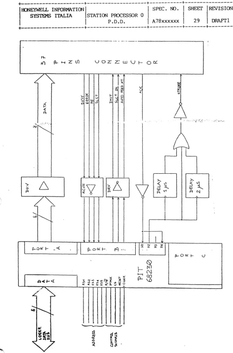
1.1.4 TIMER and PARALLEL PRINTER INTERFACE
This hardware block consists essentially of Motorola MC68230 PI/T chip, which provides a progranrnable timer plus a versatile double buffered parallel interfaces.
a) TIMER - The PI/T timer contains a 24-bit synchronous down counter that is loaded fram three 8-bit Counter Preload Registers. The 24-bit
counter·1:-.st, be clocked ···'·'by·;·the·:' , ootput'.I' of ·'a~:·s;...biti~·J(divf~a2l··
prescaler to generate periodic interrupts, a square wave, a single interrupt after a progranuned time period, or it can be used for elapsed time misurement.
Also, the end of count can be checked by software without interrupt use.
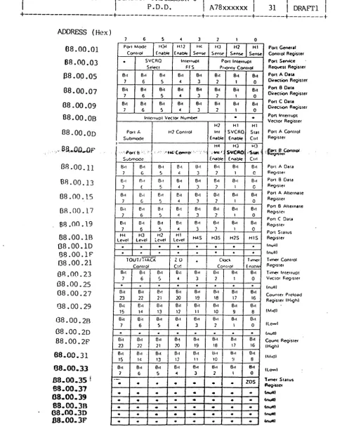
A register model that includes the corresponding Register Selects is shown in Fig. 1.1.4 .3. For further information refer to "16-BIT MICROPROCESSOR Q\TA MANUAL - 1983 MJ'IDROIA" pag. 4-509 - 4-537.
b) PARALLEL PRINTER INTERFACE - The Parallel Printer Interface allows the connection to printers with electric parallel interface both of the IBM and CENTRONICS types. Fig. 1.1.4.1 shows the major block diagram.
This interface is implemented by mean a prograrrmable parallel
interface (MC68230) plus same DRIVERs and RECEIVERs of the Low Power
Schottky type. The dialogue with the printer must be performed programming the MC68230 in the following mode:
- Port A must be set wi th Mode 0 and sutrnode 0 1 ;
- Port B must be set with Mode 0 and sutmode IX;
- all pins of the Port A must be progranmed in output mooe to
drive the printer data;
- sane pins of the Port B must be programmed in output mode to
dri ve printer ccmnand and sane ones in input mode to receive
printer status, as shown be low:
c~
(
+---+---+---+---+
I
IDNEYWELL INFORMATION \ \ SPEC. 00. SHEET REVISION \ SYSTEMS I~~ STATION PROCESSOR 0I
I
P.D.D.I
A78xxxxxx 27 DRAFTII
+---+---+---+---+---+
Pltr FORI' B MSB
7
X
6
0
(bit Input/Qutput)
5
0
4 3
0 I
ISB 2 1 0 I I I
--- BUSY:
o --)
Active1
->
No Active!. --- ERROR
o
-->
No Active1
-->
ActivePE (Paper Empty)
o
-->
Active 1-->
No ActiveSLCT
o
--> Active 1-->
No Active ---) INITo
-->
No Active 1-->
Active---) SLCT IN
o
-->
No Active 1-->
Active---) AUTO FEED XT
o --)
No Active1 --) Active
- handshake pin H4 must be used as an edge-sensitive status input pin to produce an interrupt to MC68000 when there is the trailing edge of the ACKNLG signal with the meaning of character request. The character should be sent only if the printer is ready (not busy) and no error condition is present.
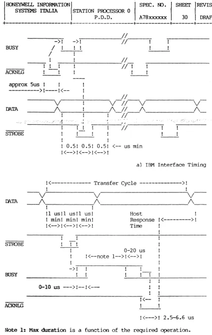
N.B. - The write of the data register (Port A) involve a hardware generation of the data STROBE signal timing without software
management necessity (see Fig. 1.1.4.2 which shows the timings relevant to CENTRONICS and IBM interfaces).
c
+---+---+---+---+
HONEYWEU. INFORMATION
I
SPEC. 00.I
SHEETI
REVISION SYSTEMS lTALIA STATION PROCESSOR 0I
P.D.D. A78xxxxxxI
28I
DRAFTI+---+---+---+---+---+
A register roodel that includes the corresponding Register Selects is shown in Fig. 1.1.4.3. For further information refer to "16-BIT
MICROPROCESSOR Jln.TA Ml\NUAL - 1983 ooroROIA" pag. 4-509 - 4-537.
The I/O signals are made available via a CANNON connector having 37 paths with female pins: the connector pin out and a detailed description of the interface signals are shown in table 1.1.4.1.
The SP board connects the printer unit via a signal cable (with
twisted-pair and shield) 5 meters max in 1enght with a 37 pin
connector at the board unit end, and a 36 pin connector on the printer
end.
The bits of the Port C are used in this way:
PI/T PORr C (bit !nput/Qutput)
MSB 7
I 6
I 5
0
4
0
LSB
3 2 1 0 0 X X X
--- NOT USED --- NOT USED --- NOT USED
--- TIMER INTERRUPT
o --)
Active1 --) No Active
!-- ---) DIAGNOSTIC INV. CHECK
o --)
No Active1 --) Active
!--->
PRINTER INTERRUPTo --)
Active1 --) No Active
!--->
PRINTER INT. ACK.o --)
Active 1 --) No Active!--->
TIMER INT. ACK.o --)
Active1 --) No Active
c
c
o
+---+---+---+---+
OONEYWELL INroRMATIONI
SPEC. 00. SHEET REVISIONSYSTEMS ITALIA STATION PROCESSOR 0
I
P.D.D. A78xxxxxx 29 DRAFTl+---+---+---+---+---+
.--._---_._---_._---_._._---,
UOZZ:WVI-OCL
1'--_~_O_rL_I-_-_.
<{ _ _--.JI-
'---_~_o_ot_I-_.
_f"1_-_,-_...J·11
~ -~
I
"'---",..,....
.,~~
I---1QJ
P-\,O
11
(
[image:29.620.54.526.10.724.2]c
,.
()
c
+---+---+---+---+
HONEYWEIL INFORMATION SPEC. 00. SHEET REVISION SYSTEMS ITALIA STATION ProcESSOR 0
P.D.D. A78xxxxxx 30 DRAFT1
+---+---+---+---+---+
~---~II----~
->! ->!
II
BUSY
I
I
II
~~~---~/I--ACKNLG
approx Sus
--->!----!<--STROBE
mTA
STROBE
BUSY
ACKNLG
II
V
V--II-V
V---"1\,~-_7_---:-'1\
II
/\ ______
--'/\ __
--11-- --11-- " '-' '-" .:...,:" ':-''-''-'''~:.:.'! -" -'-: ---:- ' •• "-1' .
---~~'.----~
II
o.S! O.S! o.S! <-- us min !<-->!<-->!<-->!
. " ~. '. ',' .'
.'
a) IBM Interface Timing
!<--- Transfer Cycle --->!
! !
--V
V
V--___
A,~---~/\.---~/\---!
!l us!l us!l us! ! min! min! min! !(-->!(-->!<-->!
Host
Response 1<--->! Time
0-20 us !<--note 1-->!<-->!
->!
0-10 us
--->1--1<---- !
! 1
1 !
1<-
-:-~---1<--->1 2.5-6.6 us Note 1: Max duration is a function of the required operation.
b) CENTRONICS Interface Timing
Fig. 1.1.4.2 Parallel Printer Interface Timing Diagram
[image:30.617.98.518.15.676.2]0
:'::.,
-';"i
0
,
..
'''", ....+---+---+---+---+
fDNEYWELL INFORMATION SPEC. 00.
I
SHEETI
REVISIONI
SYSTEMS ITALIA STATION PROCESSOR 0P.D.D. A7Sxxxxxx
I
31I
DRAFTII
+---+---+---+---+---+
:l,r
ADDRESS (Hex)
7 6 5 3 2 o
08.00.01 POtI MOde Ii).: lil2 1(<: 10 ti2 HI
COnl.ol Enable (nable S .. nsc S,,"SC S.,ns.. Sense
88.00.03
.
SVCRO InleffUOI POll tnteffu(li S .. 1e<:1 FrS P'oOf.IV COOllo/p8.00.0S B.I B.I B.I B.I B.I Bil B.I 8.t
7 6 5 < 3 2 I 0
08.00.07 Bit 8il 8il 8it 8it 8.1 8il 8it 7 6 5 4 3 2 I 0
08.00.09 Bit 8il Bil Bil Bil Bil B.I B.t 7 6 5 4 3 2 I 0
08.00.08 Inlellupl VeelOt Numbet • •
H2 HI HI
08.00.00 POtI/.. H2 ConllOl Ini SVCAO SIal
SubmOdc Enable Enable CIII.
.. ,.8B, .... OD...Df' t , .. -.>,1'011"& "". ). ~ ,':-.. :/ .... "-:.(. ... '0£.\." '( "
. "i'_"
H4 S~IIO H:; ''Sui· H3SubmOde Enable (""!>Ie CI.I
OR .00.11 B.I B'I Bol 6'1 U.I B'I B'I B'I
1 G 5 4 3 '] I C
BR.OO.13 eol fl., Bol B'I 8,1 B.I
I
8.1 B'I7 f S 4 3 7 1 0
138.00.15 8.1 Bo: B'I
I
Bit B'I Bil B'I Bil 7 (; 5 4 3 7 I 013R.OO.17 Bil B., B.I e,l B'I B'I e.1 B'I
1 6 5 ( 3 1 I 0
88.00.19 BI\ B,I B.I B'I B.I B.I 8i, B,I 7 6 5 ( j 7 1 0
88.00.1B H4 H3 H2 HI
H4S H3S H1S HIS
Level Level :"evel level
OS.OO.lD
. ·
· · ·
•·
·
138.00.lf'
.
· · · ·
· · ·
/38.00.21 TOVTnlACK za
·
C!octo. T.mer Control Clf! Con"()I (natll<I3R.OO.23 B.( 8.( B.( Bot B,( B.I B.( 801
7 6 5 4 3 2 1 0
OS.00.25
.
·
· · · ·
· ·
08.00.27 Bi( Bil B.( Bi( 8.1 8il Bil 8.t 23 22 11 10 19 18 17 16
I3S .00.29 Bil B,I Bil 8il 8il 8il 8il Bil 15 14 13 12 11 10 9 8
138.00.28 Bil 8il B.I B'I 811 B.I B,I B.I
1 6 5 4 3 2 1 0
08.00.20
. . ·
·
. · ·
·
88.00.2F Bil Bil Bil 8.,· B.I Bil B.I Bit
23 11 21 10 19 IB 17 16
68.00.31 B,I B,I B.I B.I B.I U.I B.I B.I
15 14 13 17 11 10 9 B
68.00.33 8.1 8,1 B.I B.I B.I 0,. B •• tI.t
7 6 5 4 J 2 1 0
B8.oo.35 ! . • • ZOS
·
• • •·
68.00.31
68.00.39 • • • • • • •
·
·
•
• • • • •·
88.00.38
·
·
· · ·
• •·
08.nO.3D
·
• • • •· ·
•B8.00.3F
· ·
·
· · ·
•·
('*) - Unused, read as zero.
Fig. 1.1.4.3 MC68230 Register Model
POll General
Conllol Re<,IiSler Pon Service Requesl Re<,Iisler Port ADa .. Oirection Regislef Pon 8 Date Oireelion Register Pon C Dele Direelion Reoisler POll Inierrupi Vector Regisler POll A Control Regisler
Port A Data Reg,sle, POrt B Da.a Reg,sle, Port A Alle'nale Register POri B Alterrulle Reg.).e, PO" C Dala
R~su~,
Port S.atus Regisle. (nulll Inulll Timer Conllol
R~s.e,
Time< Interrupl Veclo' Reg,sle, Invlll
Coun.e, Preload Regis.er tHigh! IModl
(Lowl Inunl Counl Aegis.e.
I Hoghl (M.dl
Ilowl
T orner SillUS
AegislCI CnuIII C ... CnuII1 tnull1 Cnultl
P~", .. IIt.1 PJ.,.I",'." .,. 7/";'~.
[image:31.617.71.559.38.663.2]('
c
+---+---+---+---+
I
HONEYWELL INFORMl\TIONI
I
SPEC. 00.I
SHEETI
REVISIONI
SYSTEMS ITALLA STATION PROCESSOR 0
I
I
P .0.0.I
A78xxxxxxI
32I
DRAITlI
+---+---+---+---+---+
Table 1.1.4.1 Parallel-Printer Connector Pin Assignment and Interface Signal Description
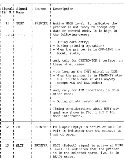
! Signal Signal !Pin N. Name
1 STROBE
2 ])l\TAO
3 ])l\TAl
4
5 ])l\TA3 6 ])l\TA4
7 ])l\TA5
8 ])l\TA6
9 oz\TA7
10 ACKNLG
Source
HOST
HOST
HOST
HOST
HOST
I HOST
HOST
HOST
Description
Data sampling strobe: it clocks data lines into the printer interface logic.! The signal level is normally HIGH;
write-out of data is performed at the LOW level of this signal. STROBE pulse width requirements are shown in Fig.
1.9.5.2 for IBM and CENTRONICS inter-faces.
o
*
Least Significant Bit (2 )These signals represent the character to be printed or the control code to be executed by the printer: normally I
these informations are given in ASCII code. Each signal is at HIGH level when data is logical "1" and LOW when
logical "0". Data Set-up and Data Hold Times requirements are shown in Fig.
1.9.5.2 for IBM and CENrRONICS inter-faces.
7 HOST
*
Most Significant Bit (2 )PRINTER Active LOW pulse. It indicates that the data has been loaded into the buf-fer or the command has been executed and that the printer is ready to ac-cept other data. In Fig. 1.9.5.2 are shown timing consideration for IBM and CENTRONICS interfaces.
[image:32.618.108.524.154.735.2]o
.:\' ..
o
0'·,
"+---+---+---+---+
IDNEYWEIL INFORMATION SPEC. 00. SHEET REVISIONI
SYSTEMS ITALIA STATION PROCESSOR 0
P.D.D. A78xxxxxx 33 DRAFT 1
I
+---+---+---+---+---+
Table 1.1.4.1 Parallel-Printer Connector Pin Assignment and Interface Signal Description (Cont'd.)
!Signal 'Pin N.
11
" .';~. '.:.~~ ':
Signal Name
BUSY
' . . J : '
12 ! PE
! !
! !
! !
! 13 SLCl'
! !
!
1
! !
Source
PRINTER
Description
Active HIGH level. It indicates the printer is not ready to accept any data or control code. It is high in the following 'cases!
- During data entry;
- During printing operation;
- When the printer is in OFF-LINE (or LOCAL) state;
and, only for CENTRONICS interface, in these other cases:
- As long as the INIT signal is LOW; - When the printer is in STAND-BY
sta-tus; in this case it will anyway accept XON and DEL codes;
and, only for IBM interface, in this other case:
- During printer error status. Timing considerations about BUSY si-gnal are shown in Fig. 1.9.5.2 for both interfaces.
PRINTER PE (Paper Empty) is active at HIGH le-vel; it indicates that the printer is out of paper.
PRINTER SLCT (Select) signal is active at HIGH level; it indicates that the printer is in the selected state, i.e. is in READY state.
[image:33.620.114.524.141.664.2]__ ",~,-,,-".;: _ _ _ ---,-__ ... -" ... ~.--:,~__ _~"""""~.~".-,~."""~""_~,~,"~_,~,,-~,,,,,,,~_~., __ -"""""'-:~_~'-'~"--C_.""---""'~~ ... , ... ,_., .. ,\,"._.
~~----~~=:~:---+---+---+---+
o
()
o
HONEYWELL INFORMATION
I
SPEC. 00. SHEET REVISIONI
SYSTEMS ITAL~ S~TION PROCESSOR 0
I
P.D.D. A78xxxxxx 34 DRAITlI
+---+---+---+---+---+
Table 1.1.4.1 Parallel-Printer Connector Pin Assignment and Interface Signal Description (Cont'd.)
!Signal Signal !Pin N. Name
14
Affi5
32
33
, I
' . ;Ir_
! !
!
!
FEED )IT
INIT
ERROR
Source Description
HOST This signal is applicable only for IBM
interface. When this signal is driven at LOW level, the paper is
automati-HOST
", :!"caUy,fed"one:1,ine 'after printing • '.'
!
For the CE~JICS interfaces this
si-gnal is named PRIME and a LOW level on this line causes the output signal BUSY to go high for as long as the INIT signal is low.
For the IBM interface, when the level of this signal becomes LOW the printer
is reset to its initial state and the printer buffer is cleared. This signal
is normally at HIGH level, and its pulse width must be m::>re than 50 us at
the receiving tenninal.
PRINTER This line is named FAULT for the
CEN-t TRONICS interface. The level of this
signal becomes LOW when the printer is in:
- PAPER END state; - OFF LINE state; - Error state.
37 ! SLCT IN HOST This signal is applicable only for Im1
interface. Data entry to the printer is possible only when the level of this signal is LOW.
1
! !
!
[image:34.620.105.541.145.646.2](~~~\
,_ ",-,""_,~_:_"_ ,.~-,-_ •• "":'_~_. __ ~,~,"...c,,-,-,,--,-__ ~~.,~, " .,;, _ _ ~~
.~c+:.::::;:;:::::=':..=::.:::::'::"::~:::::::::.:.:::.~::::::+::..:..:..:.:==:~= ___________
+ ___________ +. ________________
+HONEYWELL INFORMATION
I
I
SPEC. NJ.I
SHEETI
REVISIONI
SYSTEMS ITALIA STATION PROCESSOR 0I
P.D.D.I
A78xxxxxxI
35I
DRAFTlI
+---+---+---+---+---+
Table 1.1.4.1 Parallel-Printer Connector Pin Assignment and Interface Signal Description (Cont'd.)
!Signal' Signal Source Description !Pin N. Name
!l6-l9 GND Logic GND level.
!20-21 !22-23
!24~2.5
!26-27 !28-29 !30-31 !34
!l5-18 R.F.U. Pins not used. !35-36
17 ZVPOO Safety Ground.
HONEYWELL OONFIDb~IAL AND PROPRIETARY
[image:35.621.111.519.140.404.2]o
+---+---+---+---+
HONEYWELL INFORMA.TION
I
I
SPEC. 00.I
SHEETI
REVISION \ SYSTEMS ITALIA STATION PROCESSOR 0I
P.D.D.I
A78xxxxxxI
36I
DRAFTlI
+---+---+---+---+---+
~O ~N·rER~0~T G~0~G
1.1.5 VME BUS INTERRUPTER LOGIC (BIL)
The VME Bus Interrupter Logic allows to generate interrupts to the VME bus on any of the seven levels and supplies an 8-bit vector during interrupt acknowledge cycle. Besides it handles the daisy-chain configuration.
The heart of this logic is the SIGNETICS 68154 Interrupt Generator (IGJR) , that provides this interface between an interrupting device and the VME Bus.
Inside it has two registers:
- the INTERRUPT VECTOR REGISTER RO located at Hex E8.00.01 - the INTERRUPT REQUEST REGISTER Rl located at Hex E8.00.05
The local processor writes the interrupt vector register to generate an interrupt on any interrupt request level of the VME Bus.
The RO register has this layout: MSB
7 6 5 4 3
LSB
2 1
--- ENABLE INTERRUPT
o
--> No active 1 --> Active! ---
CLEAR INTERRUPT REQUESTo
--> No active 1 --> Active__________ . ____ I
---!
HIGH ORDER BITS OF
---!
INTERRUPT VECTOR!---!
!---!
c
c
+---+---+---+---+
I
HONEYWEIL INFORMATIONI
I
SPEC. 00.I
SHEETI
REVISIONI
SYSTEMS ITALIA STATION PROCESSOR 0I
I
P.D.D.I
A78xxxxxxI
37I
DRAFTII
+---+---+---+---+---+
The Rl register has this layout:
> ..•. i·· ! ' .
*
Register layout:~B ~B
7 6 5 4 3 2 1
1
---) IRQI:
- ' - < ;.·0··--) ,.No Active
1 --) Active ---) IRQ2:
o --)
No Active1 --) Active
---) IRQ3:
o --)
No Active1 --) Active
---) IRQ4:
o --)
No Active 1 --) Active ---) IRQ5:o --)
No .~ctive1 --) Active ---) IRQ6:
o --)
No Active1 --) Active
!---)
IRQ7:o --)
No ActiveI --) Active
The 7/6/5/4/3 bits of the interrupt vector register plus the A3 A2 Al address bits of the VME Bus foon the interrupt vector register
passed during an interrupt acknowledge cycle.
Writing a 1 to bit 2 of the RO register are reset all interrupt levels in the interrupt request register. Bit 2 will always be read as
o.
Setting bit 1 of RO all interrupt levels are enabled.
c
o
c
+---+---+---+---+
HONEYWELL INFORMATION/ / SPEC. NO. / SHEET /REVISIONISYSTEMS I~LIA STATION PROCESSOR 0
I
P.D.D.I
A78xxxxxxI
38I
DRAFTlI
+---+---+---+---+---+
Any Number ( up to seven ) of interrupt request can be generated in single access of Rl but they are not stackable on the same level. To generate another interrupt request on a level currently asserted, the user Imlst wait until that level has been acknowledge. During an interrupt acknowledge cycle the corresponding bit of the interrupt level will automatically cleared by the device.
Refers to the Signetics SCB68154 data sheet on Signetics book (January 1986 pages 2-358 2-368).
o
o
0",
, "+---+---+---+---+
HONEYWELL INFORMATIONI
I
SPEC. 00.I
SHEETI
REVISIONI
SYSTEMS ITALIA STATION PROCESSOR
a
I
I
P.D.D.I
A78xxxxxxI
39I
DRAFTII
+---+---+---+---+---+
1.1.6 A'ITENTION LOGIC AND SYSTEM FAIL DETECTION
The Attention Logic allows to generate interrupts to the MC68000 from System's CPU and supplies an 8-bit vector, loaded by the interrupting device, during interrupt acknowledge cycle.
Below are shown the registers layouts and access mode of this logic:
- ATTENTION INTERRUPT REGISTER:
*
Write/Read 8 bit register.*
Access mode:Le>_IADDRESS: F8.00.00 Hex. lh'7Jl ApDllnsS
5
<;. '33,00,0'-::,Read/Write UPPER ~TA BYTE. TAS.
*
Register layout: MSB7 6 5 4 3 2
LSB
1
a
x x x x x x
--->
NOT USED--->
NOT USED--->
NOT USED--->
NOT USED--->
NOT USED--->
~T
Wg88~
~"/~
--->
INTERRUPT:a
-->
No Active1
-->
Active---.---->
BUSY:o
-->
Free 1 --> Busyc
c
+---+---+---+---+
\HONEYWELL INFORMATION \ SYSTEMS I~IA STATION PROCESSOR 0 \ SPEC. 00. SHEET REVISION
I
I
I
P.D.D.I
A78xxxxxx 40 DRAFTlI
+---+---+---+---+---+
- ATTENTION VECTOR REGISTER
riSB
* Write/Read 8 bit register.
* Access rrode:
ADDRESS: F8.00.0l Hex;
Write/Read LOWER ~TA BYTE.
*
Register layout:7 6 5 4 3 2
[sB
1 0
The informations contained in these registers can be also supplied
at word lenght.
ltispossible to give only one interrupt at a time to the 68000
sootrJ[r~ setting the bit SIX after having checked with the TAS
instruction, the 7 bit (BQSY) of the Interrupt Register that no one
else interrupt is active.
The reset of the Interrupt Register is made by software control accessing to the interrupt register.
The system fail condition is detectable in the bit
~
of theATTENTION INTERRUPT REGISTER . The software running in the SGM2 CPU
can know which spa board in the VME Bus is in the system fail
condition.
:'::'
C
~l. . '
o
O
J ,.+---+---+---+---+
HONEYWELL INFORMATION
I
SPEC. 00. SHEET REVISIONI
SYSTEMS ITALIA STATION PROCESSOR 0
P.D.D.
I
A78xxxxxx 41 DRAFT 1I
+---+---+---+---+---+
1.1. 7 PROCESSOR NUMBER AND BOARD TYPE DETECfION
There is a register loacated at Hex A8.00.00 where is possible to
know same information about the board:
- in which slot of the SGM2 VME Bus the SPO board was inserted;
- the type of the board inserted (SPO or LPO);
~,:it.e:;~ i.ng enviroment;
The layout of this register is:
MSB LSB
7 6 5 4 3 2 1 0
---) ALWAYS 0 ---1
SPO / LPO BITS
1---1 000
=
SPO111
=
LPO---1
---~--) PROCESSOR NU~ffiER (bit 2)
---) PROCESSOR NUMBER (bit 1)
---) PROCESSOR NUMBER (bit 0)
!---)
LBT PRESENT FACTORY SIGNA.LALWAYS 1 0lIT OF TEST
c
C~
ic
- - - -".,-,,--_ •• ·U"''--'--.J...!.~
+---+---+---+---+
HONEYWELL INFORMATION SPEC. NO. SHEET REVISIONSYSTEMS I~L~ STATION PROCESSOR 0
P.D.D. A78xxxxxx 42 DRAFTl
+---+---+---+---+---+
The table below describes the VME bus addressing space of each board with the p~ssor number bits equal to:
6 5 4
0 0 0 PROCESSOR NUMBER 0 - SPO located at Hex 56.00.00.00 (VME BUS ADDRESSING SPACE)
.' . "", "
" ~ • • I ~
.,.,... , o!.: ,
1 0 0 PROCESSOR NUMBER 1 - SPO located at Hex 56.40.00.00 (VME BUS ADDRESSING SPACE) 0 1 0 PROCESSOR NUMBER 2 - SPO located at Hex 56.80.00.00
(VME BUS ADDRESSING SPACE)
1 1 0 PROCESSOR NUMBER 3 - SPO located at Hex 56.CO.00.00 (VME BUS ADDRESSING SPACE) 0 0 1 PROCESSOR NUMBER 4 - SPO located at Hex 57.00.00.00
(VME BUS ADDRESSING SPACE)
1 0 1 PROCESSOR NUMBER 5 - SPO located at Hex 57.40.00.00 (VME BUS ADDRESSING SPACE) 0 1 1 PROCESSOR NUMBER 6 - SPO located at Hex 57.80.00.00
(VME BUS ADDRESSING SPACE)
1 1 1 PROCESSOR NUMBER 7 - SPO located at Hex 57.CO.00.00 (VME BUS ADDRESSING SPACE)