Biphase Amplifier based Precision Rectifiers using
Current Conveyors
Parveen Beg
Department of Electronics Engineering,
Z. H. College of Engineering & Technology,
Aligarh Muslim University, Aligarh-202002, India
Iqbal A. Khan
Department of Electrical Engineering, Faculty of Engineering &
Islamic Architecture, Umm Al Qura University,
Makka Al Mukarrama, P. Box: 5555, Kingdom of
Saudia Arabia
Sudhanshu Maheshwari
Department of Electronics Engineering,
Z. H. College of Engineering & Technology,
Aligarh Muslim University, Aligarh-202002, India
ABSTRACT
A novel and simple circuit for precision rectifier using second-generation current conveyor (CCII) is presented in this article. The circuit basically uses a CCII-based voltage mode bi-phase amplifier, which has been used as full-wave and half-wave rectifiers. To switch the bi-phase amplifier from non-inverting to non-inverting mode, a MOSFET and a CCII-based comparator has been used. The circuit exhibits precision rectification over a wide range of operation and can also be implemented using commercially available ICs such as the AD844. The proposed circuits have been simulated using CMOS implementation of current conveyor with effective results.
General Terms
Analog Signal Processing, Electronic Circuits
Keywords
Current conveyors, bi-phase amplifier, precision rectifiers, DVCC
1.
INTRODUCTION
Precision rectifiers form an important building block in non linear analog processing systems. In such rectifiers, the threshold voltages associated with diodes are overcome and hence enable the rectification at relatively low signal levels required for signal processing applications. With the advent of current conveyors, which offer a number of advantages over other devices, many precision rectifiers using current conveyors have been recently reported in literature [1-16]. However, many of them use a complex circuitry [6-9]. In this paper, novel precision rectifiers using Second-Generation Current Conveyor (CCII) and Differential Voltage Current Conveyor (DVCC) based bi-phase amplifier are presented. The bi-phase mode of the amplifier is controlled with the help of an additional voltage controlled switch and a comparator to achieve half-wave and full-wave rectification. The proposed precision rectifier offer features such as simpler hardware and a wide frequency range of operation. Non-ideal and parasitic study of the proposed circuits is also performed. The circuit proposed is designed and verified using PSPICE.
2.
CIRCUIT DESCRIPTION
The second-generation current conveyor (CCII) symbol is shown in Fig.1, which is characterized by
X Z Y
Y
X
V
I
I
I
V
,
0
,
(1)CCII + Y
X
Z+ VZ
VY
VX
IY = 0
IX
IZ
Fig 1: The symbol of CCII
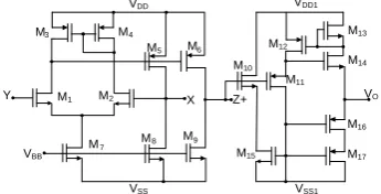
The CMOS implementation of the CCII along with a buffer is given in Fig. 2, while the realized bi-phase amplifier is shown in Fig. 3.
M2 X
M1
M3 M4
M5
M7 M8
M6
M9
Y
VBB
VDD
Z+ VDD1
M10
M11
M12
M13
M14
M16
M17
M15
VO
[image:1.595.340.513.390.478.2]VSS VSS1
Fig 2: The CMOS structure of the CCII with buffer
CCII + X
Y
Z+ V0
Vin
R1
R3 P
1 VO
R2
[image:1.595.333.524.518.608.2]S
Fig 3: CCII based bi-phase amplifier
The amplifier uses a voltage-controlled switch S. When S is open, the output voltage V0 can be expressed as:
V
0
V
in (2)When S is closed, the voltage at node P is zero. Now by selecting R2=2R1 the output voltage becomes:
V
0
V
in (3)realized with a P-MOS transistor along with CCII+ based non-inverting comparator as shown in Fig. 4.
CCII + X
Y
Z+ V0 Vin R1 R3 CCII + X Y Z+ P R4
[image:2.595.314.535.96.242.2]1 VO R2
Fig 4: Proposed precision rectifier circuit-I
2.1
Additional precision rectifier circuit
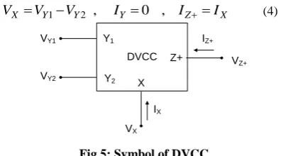
The circuit presented in this section is a modified form of the circuit shown in Fig. 3. This modified circuit employs a DVCC-based biphase amplifier. Further, the switch of the biphase amplifier is also realized using a DVCC-based comparator and a NMOS transistor. The symbol of a DVCC with only a Z+ output is shown in Fig. 5 [17], which is characterized by the following port relationship.
X Z Y
Y Y
X
V
V
I
I
I
V
1
2,
0
,
(4) [image:2.595.65.265.297.407.2]DVCC X Y2 VY1 VY2 VX Y1 Z+ V Z+ IZ+ IX Fig 5: Symbol of DVCC
[image:2.595.54.269.527.649.2]The DVCC-based precision rectifier is shown in Fig.6. Here, DVCC ② is used as a comparator [17]. During the positive half of the cycle, the comparator output is low and the switch is open thus leading to V0 = Vin. During the negative half of the cycle, the comparator output is high; the switch is closed, and thus the bi-phase amplifier behaves in an inverting mode resulting in V0 = −Vin. As a result, full-wave rectification is achieved. The advantage of this circuit over the previous circuit (shown in Fig. 4) is that one passive resistance R4 is eliminated andthePMOS transistor is replaced by an NMOS transistor which is suitable for IC fabrication in terms of area.
Fig 6: Proposed precision rectifier circuit-II
3.
NON-IDEAL ANALYSIS
3.1
Effect of transfer gain
A non-ideal CCII is characterised by
X Z Y
Y
X
V
I
I
I
V
,
0
,
(5) where is the voltage transfer gain from Y to X and α is the current transfer gain from X to Z+. Re-analysis of the firstproposed circuit of Fig. 4 using equation (5) yields the following relation:
During the positive half cycle:
1 1 11 11 11 1 2 , 0 1 2 3 2 R R V V i n (6)
During the negative half cycle:
1 1 1 2 , 0 1 R R V V i n (7)
Selecting R2 = 2R1 , equations (6) and (7) reduce to:
1 1 11 11 11 , 0 1 2 3 i n V V (8) 1 1 , 0 1 2 i n V V (9)
It is to be further noted that equations (8) and (9) reduce to
equations (2) and (3) respectively for α1 = 11 = 1.
3.2
Effect of Parasitics
A CCII is characterised by the following parasitic port impedances: The parasitics are RX, RY//CY and Rz//CZ for X-,Y- and Z ports respectively. Considering the X- and Y- terminal parasitics, the output voltage during the positive half cycle can be expressed as:
Y Y Y X Y X Y Y X X i R R C R R s R R R C R R R C s R R R R V V 3 3 2 3 1 1 2 '
0 ( )
) 2 ( 1 ) 2 ( (10)
For a typical design R3 << RY thus R3//RY≃ R3 . By selecting R2 =2R1 , equation (10) reduces to:
3 1 3 1 1 1 ' 0 1 ) 2 ( ) 2 ( 1 ) 2 ( ) 2 ( R C s R R R C R R R C s R R R R V V Y X Y X Y Y X X i (11)
During the negative half of the cycle the output voltage can be expressed as: on Y on X Y X on Y X X i r R C r R s R R R C R R r C s R R R R V V 3 3 2 3 1 1 1 '
0 ( )
) 2 ( 1 ) 2 ( ) 2 ( (12)
where ron is the ON resistance of MOSFET.
Again, in equation (12) ron << R3 thus ron // R3 ≃ ron . By selecting R2 =2R1, equation (12) reduces to:
on Y X Y X on Y X X i r C s R R R C R R r C s R R R R V V 1 ) 2 ( ) 2 ( 1 ) 2 ( ) 2
( 3 1
1 1 1 ' 0 (13) DVCC ① X Y1
Z+ V0
Vin R1 R3 DVCC ② Y2 X Z+ P
1 VO
R2
Y1
Closer inspection of equations (11) and (13) for a typical design shows that the gain of the rectified output is not affected. The pole and zero introduced due to parasitics are found to be symmetrical and approximately equal in magnitude, thus they may be the cause for certain phase errors. It is also to be noted that for open-switch as well as for closed-switch conditions (equation (11) and (13)), the path from port Y to ground will contain RY or RY//rON respectively. Therefore both equations (11) and (13) show a ‘minus’ sign.
4.
DESIGN AND VERIFICATION
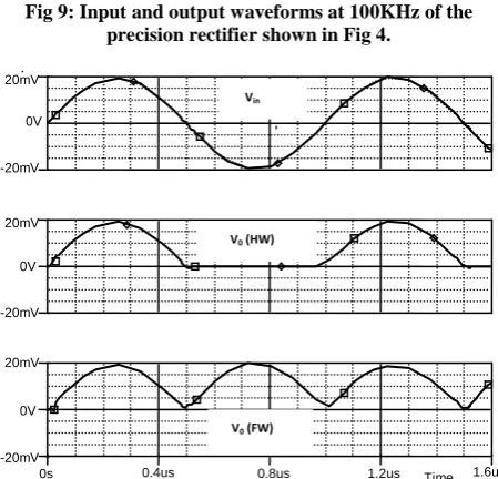
To verify the proposed theory, the precision rectifier of Fig. 4 is designed and simulated using PSPICE. The model parameters for the CMOS CCII are taken from MIETEC 0.5 µm CMOS process [18]. The PMOS switch is implemented with the W/L ratio as 7 µm /0.35 µm. For a bi-phase amplifier, selecting R1 = 1KΩ leads to R2 = 2KΩ. R3 and R4 are selected as 150KΩ and 400 respectively. The supply voltages are taken as VDD = VSS = 2.5V and VBB = 1.96V. The MOS transistors aspect ratios for the CMOS CCII are given in Table 1. The resulting DC transfer characteristics of the proposed precision rectifier are shown in Fig.7. Its performance is also verified with a sinusoidal input of 20mV peaks at 10 KHz, 100 KHz and 1 MHz, the results of which are depicted in Fig.8-10.
The proposed circuit of Fig. 6 is designed with R1 = 2KΩ, R2 = 4KΩ and R3 = 40KΩ. The supply voltages are kept as before. The NMOS transistor aspect ratio is 10 µm /0.35 µm. The full-wave rectified output at 20mV peaks and at 1 MHz are shown in Fig. 11.
[image:3.595.313.543.62.518.2] [image:3.595.318.543.73.260.2]The distortions visible during the clock switching edge at increasing frequencies are mainly due to the switching limitation of the transistor. These may be reduced by employing high frequency transistors.
Table 1. Dimensions of the transistors used in CCII Transistor W (µm) L (µm)
M1, M2 0.8 0.5
M3, M4 4 0.5
M5,M6 10 0.5
M7 14.4 0.5
M8, M9 45 0.5
Fig 7: DC transfer characteristics of the precision rectifier
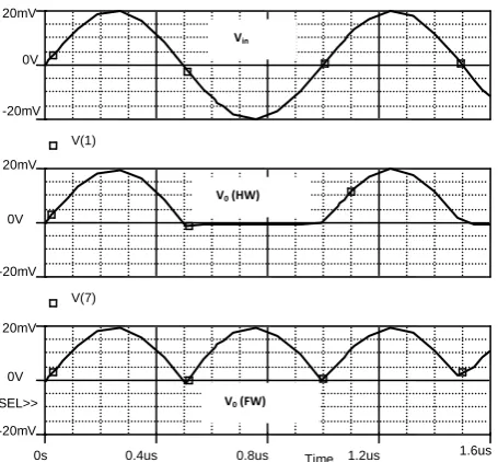
[image:3.595.315.539.290.498.2]Fig 8: Input and output waveforms at 10KHz of the of the precision rectifier shown in Fig 4.
Fig 9: Input and output waveforms at 100KHz of the precision rectifier shown in Fig 4.
Fig 10: Input and output waveforms at 1MHz of the precision rectifier shown in Fig 4.
VIN
-100mV -50mV 0V 50mV 100mV 0V
50mV
VO
U
T
100mV
Time 0s 0.4us 0.8us 1.2us 1.6us -20mV
0V 20mV -20mV 0V 20mV -20mV 20mV
0V
Vin
V0 (HW)
V0 (FW)
0s 4us 8us 12us 16us -20mV
20mV -20mV 0V 20mV -20mV 0V 20mV
0V
V0 (FW)
V0 (HW)
Vin
Time
Time 0s
40us 80us 120us 160us -20mV
20mV -20mV 0V 20mV -20mV 0V
Vin
V0 (HW)
V0 (FW)
20mV
[image:3.595.51.283.423.601.2] [image:3.595.316.541.511.727.2]Fig 11: Input and output waveforms at 1MHz of the precision rectifier shown in Fig. 6
5.
COMPARATIVE STUDY
The circuits proposed in this work were compared to similar circuits reported in literature. The different parameters used for comparison were:
i. Type of active building blocks used ii. Number of diodes
iii. Number of resistors
iv. Half-wave and/or full wave capability v. Operating frequency
vi. Signal (voltage or current) amplitude range
The results are depicted in Table 2. It may be noted that most of the available circuits are based on two current conveyors. There are some works which benefit from using only a single current conveyor or OTA [4, 9, 10, 16]. However one of these [9] exhibits only half-wave rectification. As far as the frequency range is concerned, the circuit proposed by [9] with half wave capability is quite attractive. Similarly the work proposed by [6] also exhibits good frequency performance but employs a number of diodes.
The circuits proposed by [10, 12] exhibit good precision. However the operating frequency for the latter is limited as compared to the former, though it may not be entirely fair to compare these circuits since they fall in the class of tunable precision rectifiers. However, as can be seen, the circuits proposed in this work benefit from a good precision, half wave as well as full-wave operation and a moderate to good operating frequency. Moreover, the new proposed circuits are a novel addition to the already vast literature on the subject
6.
CONCLUSION
In this work, a novel precision rectifier using second generation current conveyor is realized. The realized precision rectifier uses a CCII-based voltage mode bi-phase amplifier. To switch the bi-phase amplifier from non-inverting to inverting mode, a MOSFET switch and a CCII based comparator has been used. A DVCC based precision rectifier circuit is further introduced. Non-ideal and parasitic study is also given. The rectifier was designed and verified using PSPICE simulation. The results prove that the circuit achieves half-wave as well as full-wave precision rectification The simulated precision rectifier also exhibits a wide frequency range of operation and uses simple hardware. Improving the performance and high precision capability of the circuit is an area open for further research.
Table 2. Comparison of proposed and existing circuits
Reference No. Feature
(i) (ii) (iii) (iv) (v) (vi)
[2] 2 CCII, 2OPAMP 4 2 N/Y 100KHz ± 500mV
[4] 1 FDIO-OTA 4 1 Y/Y 500MHz ±500mV
[6] 2 CCII 4 2 - 30MHz -
[7] 2CCII 4 2 N/Y 100KHz ±100mV
[8] 1 CCII, 2 OPAMP 2 3 N/Y 100MHz ±1V
[9] CCII- - 1 Y/N 100MHz ±25mV
[10] 1 CCII, 2 MOS - 1 or 0 Y/Y 100KHz ±10mV
[11] CDTA 4 2 N/Y 5MHz ±50µA
[12] 2 CCII, 2 MOS - 2 N/Y 20KHz ±20mV
[13] 3 CCCII - - N/Y 100KHz -
[14] 3 CCII - - N/Y 1MHz ±80µA
[15] 2 CCII, 3 MOS - - - 250KHz ±50mV
[16] DXCCII, 3MOS - - N/Y 1MHz ±150mV
Proposed (Fig.4) 2 CCII, 1 MOS - 4 Y/Y 1MHz ±20mV
Proposed (Fig.6) 2 DVCC, 1 MOS - 3 Y/Y 1MHZ ±20mV
7.
REFERENCES
[1] Wilson, B. 1990. Recent development in current conveyors and current mode circuits. IEE Proc. G, 132 (2), 63-67.
[2] Gift, S. J. G. 2002. An improved precision full-wave rectifier. International Journal of Electronics, 89(3), 259-265.
[3] Khan, I. A. and Zaidi, M. H. 2000. Multifunctional translinear-C current mode filter. International Journal of Electronics, 87, 1047-1051.
[4] Kumngern, M. and Dejhan, K. 2006. High frequency and high precision CMOS full-wave rectifier. International Journal of Electronics, 93, 185-199.
[5] Khan, I. A., Khan, M. R., and Afzal, N. 2006. Digitally programmable multi-functional current mode filter using CCIIs. Journal of Active and Passive Electronic Devices, 1, 231-220.
Time
0s 0.4us 0.8us 1.2us 1.6us -20mV
0V 20mV
SEL>> V(7) -20mV
0V 20mV
V(1) -20mV
0V 20mV
Vin
V0 (HW)
[image:4.595.70.520.458.640.2][6] Toumazou, C., Lidgey, F. J., and Chattong, S. 1994. High frequency current conveyor precision full-wave rectifier. Electronics Letters, 30, 745-756.
[7] Monpapassorn, A., Dejhan, K. and Cheevasuvit, F. 2001. A full-wave rectifier using a current conveyor and current mirrors. International Journal of Electronics, 88, 751-758.
[8] Gift, S. J. G. 2000. A high-performance full-wave rectifier circuit. International Journal of Electronics, 89, 467-476.
[9] Kumngern, M. and Dejhan. K. (2007). High frequency, high precision CMOS half-wave rectifier. In Proceedings of the The ECTI International Conference, Thailand, 1-4.
[10] Maheshwari, S. 2007. Current controlled precision rectifier circuits. Journal of Circuits Systems and Computers. 16(1), 129-138
[11] Biolek, D., Hancioglu, E., and Keskin Umit, A. 2008. High-performance current differencing transconductance amplifier and its application in precision current-mode rectification. International Journal of Electronics and Communications, 62, 92-96.
[12] Maheshwari, S. and Khan, I. A. 2005. An integrable precision rectifier with current controlled output. Journal of Active and Passive Electronic Devices, 1, 172-182.
[13] Anuntahirunrat. K., Tangsrirat, W., Riewruja, V., and Surakampontorn, W. 2000. Sinusoidal frequency doubler
and full-wave rectifier using translinear current controlled conveyors. In Proceedings of Conference on Circuits and Systems (IEEE APCCAS), China. 166-169.
[14] Siripruchyanun, M. and Jaikla, W. 2006. A novel precision current-mode full-wave rectifier and class B push-pull current amplifier using BiCMOS current-controlled current conveyors. The Journal of King Mongkut's University of Technology, North Bangkok. 16(1), 1-6.
[15] Yuce, E., Minaei, S., and Cicekoglu, O. 2006. Full-wave rectifier realization using only two CCIIs and NMOS transistors. International Journal of Electronics, 93(8), 533-541.
[16] Minaei, S. and Yuce, E. 2008. A new full-wave rectifier circuit employing single dual-X current conveyor. International Journal of Electronics, 95(8), 777-784.
[17] Maheshwari, S. 2008. A canonical voltage-controlled VM-APS with a grounded capacitors. Circuit System Signal Processing, 27, 123-132.