A Low Power 90nm Technology based CMOS Digital
Gates with Dual Threshold Transistor Stacking
Technique
P. S. Aswale
M.E. VLSI & Embedded SystemsDepartment of ETC Engineering SITRC, Nashik, Maharashtra, India
S. S. Chopade
Associate Professor Department of ETC Engineering SITRC, Nashik, Maharashtra, IndiaABSTRACT
Scaling of transistor features sizes has improves performance, in-crease transistor density and reduces the power consumption. A chip’s maximum power consumption depends on its technology as well as its implementation. As technology scales down and CMOS circuits are powered by lower supply voltages, leakage current becomes significant. static power is becoming the pre-dominant source of energy waste. To create methodologies that support efficient designs, good performance, lower costs in the era of low power, is up to the design, EDA community . As the threshold voltage is reduced due to scaling, it leads to in-crease in sub threshold leakage current and hence inin-crease in static power dissipation. This paper presents performance analy-sis of inverter using conventional CMOS, stack and dual thresh-old transistor stacking techniques. The performance analysis of inverter were analyzed in 90nm technology using Cadence vir-tuoso environment. The use of dual threshold voltages can sig-nificantly reduce static power dissipated in CMOS VLSI circuits.
General Terms:
Low Power Design
Keywords:
CMOS inverter, static power, threshold voltage, transistor stacking, ULSI.
1. INTRODUCTION
[image:1.595.313.535.306.436.2]In early 1970’s, providing high speed operation with minimum area were main aim of design. Many design tools are concentrated to achieve these goals. ITRS reported that leakage power consumption may come to dominate total chip power consumption as technology feature size shrinks [7,8]. As we can observed that static consump-tion tends to increase over the year as dynamic power consumpconsump-tion [8]. The increasing prominence of portable systems and the need to limit power consumption in very high density ULSI chips have lead to rapid and innovative development in low power design. Due to power sensitive portable devices, low power is very important requirement of all high performance application where power is one of the important design constraints. In today’s era of VLSI,
Fig. 1. Power consumption prediction by the ITRS 2009[8].
not only on its technology but also on its implementation i.e on size, circuit style, operating frequency and so on. Because of this tech-nology trends transistor leakage power has increased exponentially supply voltage scaling increases sub-threshold leakage current, in-creases leakage power and pose numerous leakage in the VLSI de-sign. Therefore static power has become a significant portion of the total power consumption. There are several VLSI techniques to re-duce leakage power. Different techniques provides an efficient way to reduce leakage power, but disadvantages of each technique limit the application of each techniques. In this paper an efficient sub-threshold leakage current reduction and optimization methods are presented and result are given for 90nm generic process design kit technology using virtuoso schematic editor.
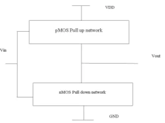
[image:2.595.87.254.326.450.2]2. REVIEW OF PREVIOUS WORK 2.1 Conventional CMOS technique
Fig.2. shows the block diagram of digital circuit using conven-tional CMOS techniques. In this technique, a fully complementary CMOS circuit has an nMOS pull down network to connect the out-put to ’0’ (GND) and pMOS pull up network to connect the outout-put to ’1’ (VDD).
Fig. 2. Base case (conventional CMOS) circuit structure.
2.2 Forced Transistor Stacking Technique
[image:2.595.56.278.565.676.2]This technique is based on the fact that natural stacking of MOS-FET helps in achieving leakage current. The leakage through two series OFF transistor is much lower than that of single transistor be-cause of stack effect [4]. An effective way to reduce leakage power in active mode is stacking of transistor [1].
Fig. 3. Forced Stack Technique circuit structure.
Fig. 4. Circuit Schematic of Forced Stack Technique[6]
The subthreshold leakage is exponentially related to the threshold voltage of the device and threshold voltage changes due to body effect. The source of the nMOS device N1 is connected to ground. Transistor N2 source is connected to drain of N1. The source of N2 is not grounded and it can acquire voltages close to Vdd while its substrate is connected to ground. Therefore the condition Vsb=0 will not hold in bias cases for transistor N2. The device N1 will experience higher Vth due to the difference in the voltage between the source and body. The voltage between drain and source also de-creased since the intermediate node has a voltage above the ground resulting reduction in DIBL affect and hence effective saving of leakage power. For turned off the single transistor,leakage current Isub0 can be expressed as follows[3,11]:
Isub0=Ae
1
nV θ(Vgso−Vtho−γVsbo+ηVdso)(1 −e
Vdso Vθ ) (1)
=AenVθ1 (−Vtho+ηVdd) (2)
A=µ0Cox(W/Lef f)Vθ2e1.8 (3)
n=sub-threshold coefficient V=thermal voltage Vgs0, Vth0, Vbs0 and Vds0 are the gate-to-source voltage, the zero-bias threshold voltage, the base -to-source voltage and the drain-to-source volt-age respectively.γis the body-bias effect coefficient, andηis the Drain Induced Barrier Lowering (DIBL) coefficient.µiszero-bias mobility, Cox is the gate-oxide capacitance, W is the width of the transistor, and Leff is the effective channel length.
Two transistor are turned off together (M1=M2). So,
Isub1=Ae
1
nVθ(Vgs1
−Vtho−γVsb1+ηVds1)(1−e vds1
Vθ ) (4)
=AeηVθ1 (−Vx−Vtho−γVx+η(Vdd−Vx)) (5)
Isub2=Ae
1
nVθ(Vgs2
−Vtho−γVsb2+ηVds2)(1−e Vds2
Vθ ) (6)
=Aenvθ1 (−Vtho+γVx)
(1−e−Vx/Vθ) (7)
Where Vx is the voltage at the node between M1 and M2. Now consider X is the factor of Isub0 and Isub1 (==Isub2)
X= Isub0
Isub1
= Ae
1
nV θ(−Vtho+ηVdd)
AenVθ1 (−Vx−Vtho−γVx+η(Vdd−Vx))
=eηVθVx(1+γ+η)
If Isub1=Isub2 then from equation (4.8) we can write,
1 =enVθ1 (ηVdd−Vx(1+2η+γ))
+e−VθVx (9)
Threshold voltage can be controlled by body bias effect.
Vth=Vt0+γ( p
Vsb) (10)
Changing the substrate voltage causes the threshold voltage to change. So the different kind of effect is arises for changing the substrate voltage like Zero-Body Bias, Reverse-Body Bias and Forward-Body Bias. This Phenomenon is frequently used for con-trolling the threshold voltage.γconstant dependent on the transis-tor parameter and the technology feature size. By controlling body biasing effect with changing the constant term we can easily control the leakage power[3,10].
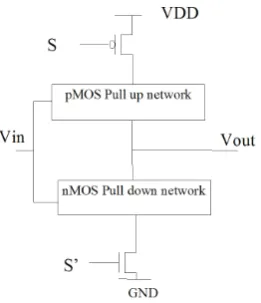
2.3 Sleep Transistor Technique
[image:3.595.381.463.105.229.2]This technique uses the sleep transistor between both VDD and the pull up network and between GND and pull down network [3]. The sleep transistor turn off the circuit by cutting off the power rails in idle mode thus can reduce leakage power effectively.
Fig. 5. Sleep Transistor Technique Structure.
In this technique we have floating values and thus will lose state during sleep mode. The Wakeup time and energy of the sleep tech-nique have significant impact [3]. The techtech-nique in which high Vth sleep transistor are used called Multi-threshold voltage CMOS (MTCMOS) proposed by Motoh et al. [3].
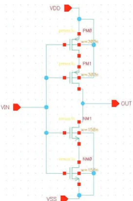
2.4 Dual Threshold Transistor Stacking Technique This new technique called dual threshold transistor stacking hy-brid version of stack and MTCMOS. It takes the advantage of both above techniques i.e. sleep transistor are redesigned with stack ef-fect. The size of sleep transistor is reduced. The sleep transistors are designed as a high threshold voltage [1]. Fig.6 shows the circuit schematic of Dual threshold transistor stacking technique.
3. SIMULATION RESULTS
Simulations have been performed using virtuoso in 90nm gpdk CMOS technology with supply voltage 1.2V to estimate the power consumption. The Inverter and two input NAND circuit are cho-sen to compare the different techniques. The propagation delay is
Fig. 6. Dual Threshold Transistor Stacking Technique.
measured at 1kHz frequency. The resulting schematic diagram and output waveforms are shown from fig. 7 to fig. 10.
Table 1 :Physical aspects of MOS transistor using CMOS techniques Physical Aspects nMOS Transistor pMOS transistor Channel width(µm) 0.3 0.6
Channel length(µm) 0.1 0.1 Aspect Ratio 3 6
Table 2 : Physical aspects of MOS transistor using stack techniques Physical Aspects nMOS Transistor pMOS transistor Channel width(µm) 0.15 0.3
Channel length(µm) 0.1 0.1
Aspect Ratio 1.5 3
Table 3: Physical aspects of MOS transistor using DTTS techniques Physical Aspects nMOS Transistor pMOS transistor Channel width(µm) 0.15 0.3
[image:3.595.104.235.328.480.2]Channel length(µm) 0.1 0.1 Aspect Ratio 1.5 3
[image:3.595.366.480.514.652.2]Fig. 8. Inverter with Forced Stack technique.
[image:4.595.99.238.343.467.2]Fig. 9. Inverter with Sleep Transistor technique.
Fig. 10. Inverter with Dual Threshold stack transistor tech-nique.
[image:4.595.113.222.501.661.2]Fig. 11. NAND with Conventional technique.
Fig. 12. NAND with Forced Stack technique.
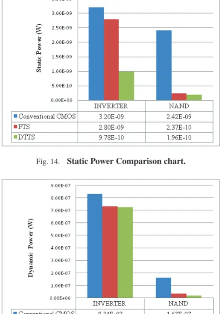
[image:4.595.324.524.520.676.2]Fig. 14. Static Power Comparison chart.
[image:5.595.58.278.480.647.2]Fig. 15. Dynamic Power Comparison chart.
Fig. 16. Propagation Delay Comparison chart.
4. CONCLUSION
The CMOS inverter is most important and used in all digital as well as analog applications. The optimization of the inverter
be-comes very important. The leakage power is of great concern for designs in nanometer technologies. As the technology scaling goes below 90nm, the standby leakage power dissipation has become a critical issue. To reduce the standby leakage power, this paper has presented a novel design technique. The results show the proposed technique is a viable solution for high energy reduction in CMOS circuits. In proposed technique no area penalty demand compared to force stack technique. The DTTS technique may be considered as an alternate for FTS technique. Power reduction varies with dif-ferent techniques. The optimization of leakage power subjects to performance metrics and active area increase constraints. This tech-nique mentioned in this paper can be implemented in low power VLSI circuit and reduce the power consumption of the chip which will increase battery life. For our Future work,we plan to calcu-late the area of the various approaches using layout and design of various combinational and sequentially circuits using proposed method.
5. REFERENCES
[1] R. Udaiyakumar, K. Sankaranarayanan, “Dual Threshold Transistor Stacking (DTTS) - A Novel Technique for Static Power Reduction in Nanoscale Cmos Circuits’, European Journal of Scientific Research, ISSN 1450-216X Vol.72 No.2 (2012), pp. 184-194.
[2] Jagannath Samanta, Bishnu Prasad De, Banibrata Bag, Raj Kumar Maity, “ Comparative study for delay & power dis-sipation of CMOS Inverter in UDSM range”, International Journal of Soft Computing and Engineering (IJSCE) ISSN: 2231-2307, Volume-1, Issue-6, January 2012.
[3] Jun Cheol Park and Vincent J. Mooney III,“ Sleepy Stack Leakage Reduction”, IEEE transactions on very large scale integration (VLSI) SYSTEMS, VOL. 14, NO. 11, November 2006.
[4] Neil Weste, Harris, Banerjee, “ CMOS VLSI Design, a circuit and system Perspective”..
[5] Sung-Mo Kang and Yusuf Leblebici, “CMOS Digital Inte-grated Circuits Analysis and Design”.
[6] Chuck Hawkins and Jaume Segura, “Introduction to Digital Electronics”.
[7] International Technology Roadmap for Semiconductors by Semiconductor Industry Association, 2009. [Online]. Avail-able http://public.itrs.net.
[8] Gerson Scartezzini, Ricardo Reis, “Using Transistor Net-works to Reduce Static Power in CMOS Circuits”, SIM 2011 - 26th South Symposium on Microelectronics.
[9] Cadence Design Systems, http://www.cadence.com/. [10] R.Udaiyakumar , K. Sankaranarayanan, “ Certain
Investi-gations on Static Power Dissipation in various Nano-Scale CMOS D Flip-Flop Structures” , International Journal of En-gineering and Technology Volume 2 No. 4, April, 2012. [11] Bipul C. Paul, Amit Agarwal, Kaushik Roy,“Low-power
![Fig. 1.Power consumption prediction by the ITRS 2009[8].](https://thumb-us.123doks.com/thumbv2/123dok_us/8095999.786170/1.595.313.535.306.436/fig-power-consumption-prediction-by-the-itrs.webp)