Simulation of interconnections in high speed integrated
circuits.
PARKER, Bruce H.
Available from Sheffield Hallam University Research Archive (SHURA) at:
http://shura.shu.ac.uk/20187/
This document is the author deposited version. You are advised to consult the publisher's version if you wish to cite from it.
Published version
PARKER, Bruce H. (1994). Simulation of interconnections in high speed integrated circuits. Doctoral, Sheffield Hallam University (United Kingdom)..
Copyright and re-use policy
3 i 4 -0 &?
ProQuest Number: 10700832
All rights reserved
INFORMATION TO ALL USERS
The quality of this reproduction is dependent upon the quality of the copy submitted.
In the unlikely event that the author did not send a com plete manuscript and there are missing pages, these will be noted. Also, if material had to be removed,
a note will indicate the deletion.
uest
ProQuest 10700832
Published by ProQuest LLC(2017). Copyright of the Dissertation is held by the Author.
All rights reserved.
This work is protected against unauthorized copying under Title 17, United States C ode Microform Edition © ProQuest LLC.
ProQuest LLC.
789 East Eisenhower Parkway P.O. Box 1346
Simulation of Interconnections in High-Speed
Integrated Circuits
Bruce Howard Parker
A thesis submitted in partial fulfilment of the
requirements of
Sheffield Hallam University
for the degree of Doctor of Philosophy
Acknowledgements
Firstly I would like to acknowledge the support given to me by the Engineering and Physical Sciences Research Council (EPSRC), and the School of Engineering Information Technology, for providing the necessary equipment to make this work possible.
Many thanks are due to my director of studies, Prof. A. K. Ray, for giving me complete freedom whilst undertaking the research documented in this thesis. Much credit is also due to my second supervisors, Prof. C. A. Hogarth, Dr. C. Johnston and Dr. Z. Ghassemlooy, for many fruitful discussions.
Abstract
The rapid development of high-speed, high-density integrated circuits has brought about a situation where the delay times and distortion of signals transmitted on the interconnections (microstrip lines) within these packages are now comparable with those of the devices in the circuit. Hence when designing high-speed digital systems the effect of signal delay, distortion, and attenuation, on these interconnections has now become a necessary part of integrated circuit design. Therefore accurate modelling and simulation of interconnects is a very important subject for research.
These interconnections can create a number of problems such as signal delay, distortion, attenuation, and crosstalk between lines of close proximity. These microstrip lines have the same behaviour as exhibited by transmission lines and can therefore be described using the well-known Telegrapher's equations.
A quasi-distributed equivalent circuit model describing the behaviour of such microstrip lines is implemented into the SPICE circuit simulator. This allows an investigation into lossless and lossy line characteristics and illustrates the importance of choosing the correct impedances for both the lines and devices within the integrated circuit package. The model is then extended to include crosstalk between neighbouring lines, by means of a transformation network. This study of crosstalk illustrates that logic functions lying in an intervening space between the pulse-activated lines are found to be affected more than the outside lines.
The MATHEMATICA package is used for the calculation of capacitance, inductance, impedance, time delay and transformation network control parameters for any set of microstrip lines of a given geometry. The results obtained from these calculations are then used for further simulation runs using the SPICE software for different line configurations.
Declaration
Table of Contents
Acknowledgements... iii
Abstract... iv
Declaration... v
Table of Contents... vi
Chapter 1 Introduction...1
1.0 : Introduction...2
Table for Chapter 1... 5
Figure for Chapter 1... 7
Chapter 2 Literature Review...9
2.0 : Introduction...10
2.1 : Microstrip Transmission Lines...12
2.2 : Computer Aided Analysis... 18
2.3 : Single Microstrip Line...19
2.4 : Coupled Microstrip Lines...23
2.5 : Skin Effect...26
Figures for Chapter 2 ... 30
Chapter 3 Background Mathematics...33
3.0 : Introduction...34
3.1: Impedance of a Single Microstrip Line...34
3.2.1 : Even mode capacitance...35
3.2.2 : Odd mode capacitance... 36
3.3 : Parameters of a Coupled Microstrip Pair...37
3.3.1 : Evaluation of self and mutual capacitance...37
3.3.2 : Calculation of self and mutual inductance...38
3.3.3 : Evaluation of impedance...38
3.4 : Inclusion of Strip Thickness... 39
3.4.1 : Evaluation of impedance...39
3.4.2 : Calculation of effective dielectric...40
3.4.3 : Effect upon odd mode capacitance...41
3.5 : Impedance and Time Delay of n Microstrips...41
3.5.1 : Capacitance matrix calculation...42
3.5.2 : Calculation of inductance matrix...43
3.5.3 : Matrix diagonalisation... 44
3.5.4 : Determination of time delay and impedance... 45
Figures for Chapter 3 ...47
Chapter 4 Ideal Transmission Line...50
4.0 : Introduction...51
4.1 : Electrical Characteristics of Transmission Lines... 51
4.1.1 : Two-wire transmission line...51
4.1.2 : Equivalent circuit...52
4.1.3 : Characteristic impedance... 52
4.2 : Propagation of DC Voltage Along a Transmission Line...55
4.2.1 : Physical explanation of propagation...55
4.2.2 : Velocity of propagation... 56
4.3 : Loading of the Line...58
4.3.3 : Resonant lines...59
4.3.4 : Reflection Coefficient (p) ...60
4.4 : Limits of Load Impedance...61
4.5.1 : Open circuit load impedance... 61
4.5.2 : Short circuit load impedance... 63
4.5 : Discontinuities ...64
4.5.1 : Effect of a step change in line width... 64
4.5.2 : Bent microstrip line... 66
4.5.3 : Multiple line intersections...67
Figures for Chapter 4 ...70
Chapter 5 SPICE Equivalent Circuit Modelling... 91
5.0 : Introduction... 92
5.1 : Ideal and Lossless Transmission Line Model...93
5.1.1 : Equivalent circuit model...93
5.1.2 : Comparison with SPICE ideal line model...95
5.1.3 : Input and output load mismatches...95
5.2 : Lossy Transmission Line Model... 98
5.2.1 : Lossy line simulation results...98
5.3 : Coupled Line Models... 99
5.3.1 : Development of coupling network... 100
5.3.2 : Application of coupled line model... 101
5.3.3 : Simulation results... 101
5.4 : Risetime Effects... 103
5.4.1 : Step input analysis ...103
5.4.2 : Effect upon pulse shape...104
5.4.3 : Coupled line effects...106
5.5 : Skin Effect Model... 107
5.5.1 : Development of skin effect equivalent circuit model...108
5.5.2 : Analysis of results... 109
5.6 : Summary... 111
Figures for Chapter 5 ... 113
Chapter 6 Mathematica Calculations...183
6.0 : Introduction...184
6.1 : Single Microstrip Line...184
6.1.1 : Impedance for zero line thickness... 184
6.1.2 : Effect of the inclusion of line thickness...185
6.2 : Coupled Microstrip Line Pair... 186
6.2.1 : Even mode capacitance... 186
6.2.2 : Odd mode capacitance... 186
6.2.3 : Even mode impedance... 187
6.2.4 : Odd mode impedance...187
6.2.5 : Impedance calculations... 188
6.3 : n Coupled Lines... 188
6.3.1 : Three coupled lines...189
6.3.2 : SPICE transient analysis...190
6.4 : Summary... 190
Tables for Chapter 6...192
Figures for Chapter 6 ... 199
Chapter 7 Conclusion...220
7.0 : Concluding Remarks...221
7.1 : Possible Further Work...224
Appendix A
Program Listing for Mathematica Calculations 1
Appendix B
Listing of Fortran Program for SPICE Equivalent Circuit Setup...9
Appendix C
Published Paper...23
1.0 : Introduction
The rapid development of high-speed, high-density integrated circuits has brought about a situation where the delay times and distortion of signals transmitted on the interconnections (microstrip lines) within these packages are now comparable with those of the devices in the circuit. Hence when designing high-speed digital systems the effect of signal delay, distortion, and attenuation, on these interconnections have now become a necessary part of integrated circuit design. Therefore accurate modelling and simulation of interconnects is a very important subject for research.
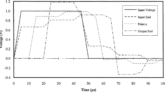
For the development of high-velocity logic circuits with a large scale integration, it is necessary to characterise the effects of interconnections, in the time domain, for signals having a rise time of about lOps. These interconnections are microstrip conducting lines because they are compatible with a planar technology and the VLSI. The distortion of the signals are essentially due to losses (in the conductors and the substrate), to impedance discontinuities (at the line endings, at the changes of section or level, when the lines are crossing), and to coupling effects between the different lines.
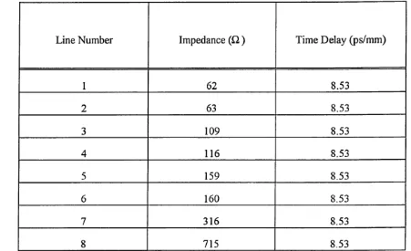
To allow a comparison of results and verification of the method used, with those from previously published work, an example of an eight line bus has been chosen (Chilo and Amaud 1984), which is depicted in figure 1.1. The eigenmodes (characteristic impedance and time delay) for each of the eight lines are given in table 1.1. This particular example was chosen because it can be used to evaluate the development of the coupled line equivalent circuit model, and for the investigation of the effects of rise time, upon coupled line configurations.
which the electrical parameters (impedance and propagation velocity) can be calculated, and how different loss mechanisms (dielectric loss and skin effect) may be employed into the method. Different types of time domain and frequency domain modelling techniques (circuit simulators and numerical methods) are reviewed.
All the relevant background mathematics necessary for the calculation of impedance and time delay for a single line and a pair of coupled microstrip lines, are discussed in chapter 3. A generalised method for the calculation of the impedance and time delay for n
coupled parallel microstrips is also developed.
A detailed study of ideal transmission lines is given in chapter 4, discussing how the time delay and impedance of the lines are related to the capacitance and inductance of the transmission line. Reflection diagrams are used to explain by the use of appropriate examples, the behaviour of various types of discontinuities which may be encountered in the design of microstrips within a high-speed IC.
Chapter 5 illustrates the development of a SPICE equivalent circuit model for the simulation of a lossless transmission line and its further development into a lossy line model. The coupling between a set of parallel microstrips is then considered. An appropriate transformation network is used in the development of an equivalent circuit model for the simulation of coupling between any set of n transmission lines. An investigation into crosstalk and the effect of rise time upon the coupling between lines, using the example given above, is also presented. The lossy equivalent circuit model is then modified for the study of the skin effect.
(Belahrach 1990) is used for the evaluation of these calculations. The results obtained are then used for SPICE simulations to in order to validate the generalised method for n
coupled transmission lines.
Line Number Impedance (Q ) Time Delay (ps/mm)
1 62 8.53
2 63 8.53
3 109 8.53
4 116 8.53
5 159 8.53
6 160 8.53
7 316 8.53
[image:16.612.64.515.224.499.2]8 715 8.53
Table 1.1: Eigenmode characteristics for the eight line bus example.
<N
ca
00
8
[image:17.627.91.750.125.437.2]2.0 : Introduction
During the seventies an important shift took place in the design of hardware with the advent of smaller and denser integrated circuits and packages. Previously, the hardware components consisted of both physically and electrically large discrete components. Stray elements and coupling among the components were small in most cases and the interconnections between the components were electrically insignificant. The corresponding electrical network models were therefore highly decoupled with sparse network analysis matrices. This led to simple analysis models and techniques for the electrical performance of these systems.
Modem technology has however shown an increasing trend towards faster circuits, shorter rise times, and smaller pulse widths (Schutt-Aine and Mittra 1989, Deutsch et al
1990). At the same time, the physical dimensions of modern integrated circuits and packages are becoming ever increasingly smaller (Ruehli 1979, Deutsch et al 1990). This technology has resulted in very high speeds such that the behaviour of the interconnections can no longer be neglected. These integrated circuits now have delay times that are comparable with the delays of the interconnections used in packaging these circuits. This means that the transmission line properties of these interconnects need to be taken into account.
Furthermore, due to the resistive nature of the interconnections used in some of these devices, the transmitted signal pulses can exhibit attenuation and distortion of considerable magnitude (Groudis 1979, Liao et al 1990). Hence when designing high speed digital systems, both the components and their interconnections must be considered or the system performance may be impaired. This has led to accurate modelling and simulation of propagation delays and signal distortion apparent on interconnection lines becoming increasingly more important in the design of high speed integrated circuits.
The advances being made in circuit density and speed, both at the chip and package level, are placing increasing demands on the performance of interconnection technologies. Designers are reducing the wiring cross-sections and trying to pack the lines closer together, whilst at the same time the propagated signals are being switched with faster rise times. The proximity of the lines to each other may result in a significant amount of cross coupling (Palusinski and Lee 1989, Van Deventer et al 1994) between the different lines, for which accurate modelling and simulation are also necessary.
The losses and coupling among a group of physically close transmission lines are important factors, especially when high density IC interconnects are considered. The combination of these two parameters gives rise to four basic models (Chowdhury et al
1992) for simulating transmission lines:
1. uncoupled lossless. 2. coupled lossless. 3. uncoupled lossy. 4. coupled lossy.
These models offer various degrees of complexity in terms of interfacing transmission lines with non-linear active devices and computing the transient response of the IC circuit as a whole. Frequency dependent transmission line behaviour, such as skin effect (Wheeler 1942) adds to the complexities already encountered in the basic models.
Considering the losses apparent on a transmission line poses many problems (Pucel et al
A general description of the electrical properties of an interconnection line (assuming transmission line characteristics), requires four parameters (Yaun et al, 1982):
1. line capacitance. 2. line inductance. 3. series resistance. 4. shunt conductance.
In integrated circuits, where only high quality insulators are used, the component of shunt conductance can generally be neglected without losing generality (Deutsch et al
1990). The series resistance can however be of significant importance as it is determined by the material from which the interconnection is manufactured. Hence, only the capacitance and the inductance reflect the properties of the substrate on which the interconnects have been fabricated.
For guidance in the design of integrated circuit components, data are required on the parameters of coupled pairs of microstrip transmission lines. The parameters needed to characterise such a structure are the characteristic impedance and propagation velocity of the two normal propagation modes; transverse electric and transverse magnetic (Djordjevic et al 1987). It is also necessary to know how the characteristic impedance, phase velocity and attenuation of the dominant microstrip mode depends on geometrical factors, electrical properties of the substrate and conductors, and on the frequency.
2.1 : Microstrip Transmission Lines
The term "microstrip" is a nickname for a microwave circuit configuration that is constructed by printed circuit techniques, modified where necessary to reduce loss, reflections, and spurious coupling, but retaining advantages in size, simplicity, and reliability (Schneider 1969). The microstrip however shares some of the troublesome
properties of dispersive waveguides, in that conductor dimensions influence not only characteristic impedance, but also the velocity of propagation (Pucel et al 1968, Gupta et al 1979).
Microstrip transmission lines, consisting of a conductive ribbon attached to a dielectric sheet with conductive backing, are widely used in both microwave and computer technology. During the 1960's the design of equipment employing microstrip lines was, however, hampered by the lack of ability to predict the electrical transmission properties of such lines, especially their characteristic impedance and wave propagation velocity. Therefore it became essential to consider the geometry of the microstrip lines in order that the electrical properties can be modelled as accurately as possible.
Given a single line or set of coupled lines, (e.g., a set of microstrips on a printed circuit board or in an integrated device) capacitance and inductance matrices can be numerically computed once the geometries of the lines and the dielectric constant of the inhomogeneous coupling material are given and the transverse electromagnetic (TEM) mode of signal propagation is assumed. Algorithms to compute these parameters, and those concerning the impedance and propagation delay, are well known with many articles having been published on the subject (Gupta et al 1979, Silvester 1968).
A microstrip line is a parallel, two-conductor line that is made of at least one flat strip of small thickness. For mechanical stability the strip is deposited on a dielectric substrate which is usually supported by a metal ground plane (Long and Butner 1990). The basic configuration is shown in Figure 2.1.
(1) The propagating mode is a transverse electromagnetic (TEM) mode, or it can be approximated by a TEM mode.
(2) Conductor losses in the metal strips are predominant, which means dielectric losses can be neglected.
(3) The relative magnetic permeability of the substrate material is fir = 1.
In order to describe the propagation of electromagnetic waves along any transmission structure, it is necessary to specify both, the characteristic impedance, Z0, and the propagation coefficient of the structure. At a first approximation perfect conductors are assumed, so that the propagation coefficient is uniquely specified by the velocity of propagation v The characteristic impedance is related to v by
where C is the electrostatic capacitance per unit length of the transmission line.
In order to determine the characteristic impedance and propagation velocity of the line, it is also important to note that
(2.1)
(2.2)
From equations (2.1) and (2.2) it follows that
Z - (2.3)
where C0 is the capacitance that the line would exhibit if the dielectric possessed unit relative permittivity (i.e. air suspended line) and c represents the speed of light in a
vacuum.
In Figure 2.2 the conductor geometry is assumed to be defined by a strip width W, a ground plane spacing h, and a small strip thickness t. It is also assumed that this is an air line with a characteristic impedance Z0, a wavelength A0, an attenuation per unit
length a0, and an unloaded Q0. For the line shown in Figure 2.1 with a dielectric support material having a relative dielectric constant the new line parameters are given by
m (2.5)
(2.6)
Q = a =
In (10) (Xq A0(2.7)
The effective dielectric constant £rc has to be measured or computed as in equation (2.8) (Ross and Howes 1976, Bahl and Garg 1977).
e + \ e - \ ( . 10 h'~'12
= - L - — + —
It is also found that the effective dielectric constant is related to the capacitance (John and Arlett 1974) of the microstrip line as follows (Schneider 1969):
C , x
From equations (2.2) and (2.9) the velocity of propagation in a single microstrip line is given by
Vp= K (2.10)
For a very narrow strip (W « h) and a very wide strip (W » h) the characteristic impedance is given by (Schneider 1969)
Z0 = 60 In 8h)
\ W j a ( w « h) (2.11)
Z„ = 120 nh
W
a
(w»h)
(2.12)Useful expressions given in terms of rational functions or series expansions can be obtained by generalisations of equations (2.11) and (2.12) as follows
Z0 = 60 In V a f —
n (
w<h
)
(2.13)^0 = J 20Z s n a (W > h) (2.14)
2>„ff
«=iwhere an and bn are terms of the series expansion. The number of terms used in the series determines the accuracy of the approximations. Equations (2.15) and (2.16) give an accuracy of ± 0.25 per cent for 0 < W/h <10, this being the range of importance for most engineering applications (Gupta et al 1979).
(2.15)
Z, =
'0 120 ;rh (, h
Y
b 1 —
---w \ ---w)
h(2.16) — + 2.42 - 0.44
h
This is however based on the assumption that the microstrip line is of zero thickness. The inclusion of strip thickness into the calculation is important, having the effect of lowering the impedance of the line. This phenomenon can be taken into account by adding an extra term to the expression for the effective permittivity (Ross and Howes 1977).
recognised in several publications (Gunston and Weale 1969, Bahl and Garg 1977).
A large number of investigations have been carried out in order to study the characteristic impedance of a microstrip line, using numerical methods. One such method is based on the application of Fourier and variational techniques (Yamashita and Mittra 1968, Yamashita 1968). It is has been shown that the impedance, velocity, and attenuation can be determined by calculating the field distribution surrounding a microstrip line bounded by a shielding wall (Stinehelfer 1968, Krage and Haddad 1970). Two other methods used for calculating the impedance of a microstrip line are the method of moments (Farrar and Adams 1970 & 1971) and the method of lines (Nam et
[W/h< 2) (2.17)
(W/h> 2) (2.18)
al 1989).
The Green's function (Collin 1960, Rickayzen 1980, Ishimaru 1991) has been used in several publications for the calculation of the impedance (Bryant and Weiss 1968, Silvester 1968, Hill et al 1969, Gladwell and Coen 1975, Cheng and Everard 1991) of a microstrip and the capacitance (Kammler 1968, Weeks 1970, Patel 1971, Silvester and Benedek 1972(a) & 1972(b), Balaban 1973, Benedek 1976, Vu Dinh et al 1992) associated with a microstrip structure.
2.2 : Computer Aided Analysis
The type of analysis required for a particular system depends on its performance and purpose. The electrical analysis may be a very simple one for low speed and low frequency circuits since the reactance of the capacitances is high and the inductances may be assumed to be short circuits. For this a simple analysis may suffice involving only the key capacitances, resistances, or inductances. In contrast, complex models are required to represent high speed and high performance systems, where the analysis may involve a large number of components.
The signal transitions in very low speed digital systems may be in the micro- or even millisecond range. Conversely at the other end of the spectrum, we may be concerned with the analysis of a very high speed logic circuit where the signal transitions may be in the picosecond range (Chilo and Amaud 1984, Hasegawa and Seki 1984, Seki and Hasegawa 1984, Schutt-Aine and Mittra 1989, Qian and Yamashita 1993, Son et al
1994).
A rigorous analysis of multiconductor transmission lines is veiy involved, especially if the response at high frequencies is to be properly evaluated (Krage and Haddad 1972, Djordjevic et al 1987). First a real multiconductor transmission line is most frequently
embedded in an inhomogeneous medium, and thus the waves propagating along the line are not of a transverse electromagnetic (TEM) nature. However even if the medium is homogeneous, due to losses in the conductor, the line is unable support TEM waves (Pucel et al 1968, Zysman and Johnson 1969, Djordjevic et al 1987).
At very high frequencies (in the microwave region), the cross sectional dimensions of the line become comparable to the wavelength of the propagating signal, allowing higher order (non TEM) modes to propagate (Djordjevic et al 1987). Secondly the analysis becomes complicated further if the influence of discontinuities (Tripathi and Bucolo 1987, Chen and Gao 1989, Orhanovic et al 1990, Zheng and Chang 1990, Sabban and Gupta 1992) (present at line ends, bends, crossovers, etc.), or nonuniformity of microstrips (Palusinski and Lee 1989, Mao and Li 1991, Dhaene and De Zutter 1992, Schutt-Aine 1992) (e.g. tapered) are to be included. Finally to evaluate the response of a transmission line terminated by arbitrary networks, which are generally non-linear (e.g. active components) with memory (i.e. contain capacitors and inductors), it is necessary to consider every part of the system simultaneously.
A survey of computer-aided electrical analysis of integrated circuit interconnections has been published (Ruehli 1979) providing a comprehensive analysis of techniques being employed to simulate microstrip interconnects. Although microstrip lines do not support signals of a TEM nature, they are generally simulated using TEM waveforms, which give a very good approximation. This is known as the quasi-TEM wave approximation (Gladwell and Coen 1975, Paul 1975, Chowdhury et al 1992).
2.3 : Single Microstrip Line
equations can be used to describe n uniform transmission lines (Paul 1973).
(2.19)
and
(2.20)
where v(x,/) and i(x,f) are the voltage and current respectively at each point x along the line at a time /.
The method of characteristics has been used (Branin 1967) to provide a simple analytic solution for the transient analysis of a uniform lossless transmission line. For solving these equations the method of characteristics is based on a transformation in the x-t plane which accomplishes the conversion of the telegraph equations (2.19) and (2.20) into a pair of ordinary differential equations. The transformation uses the equations:
which define the characteristic curves for the forward and backward waves. When L and C are constant the characteristic curves are straight lines and the phase velocity l/VLC is constant. By appropriately combining these relations with equations (2.19) and (2.20), the differential equations (2.22) and (2.23) may be derived. The forward characteristic of the line being:
(2.22)
and the backwards characteristic given by
'c dx + dv = 0 (2.23)
Equations (2.22) and (2.23) hold true along different families of characteristic curves in the x-t plane; one family corresponding to the forward or incident wave and the other to the backward or reflected wave. It is not possible for these equations to be directly integrated (Branin 1967). However if these equations are used for the case of the lossless transmission line, where R = 0 (i.e. no resistive loss in the conductor) and G = 0 (i.e. no conductance between the microstrip and the ground plane), these equations can be directly integrated, yielding exact solutions of the form Av = + Z0 Ai and A v= -Z 0 A/, where the characteristic impedance of the line Z0 = -y/L/C. This leads to an efficient algorithm that yields not only the input and output responses but also the incident and reflected waves.
Many papers have been published concerning the analysis of a single lossy line in the time domain where the series resistance of the conductor is taken into account (Schreyer et al
1988). The conductance may also be taken into consideration (Chang 1990), but is not essential for an accurate lossy line model. The transient response of uniform RLC transmission lines has been studied (Cases and Quinn 1980), where the case of a general RLC transmission line was investigated, with specific reference to a line with low total series resistance.
A lossy transmission line model (Groudis 1979) has been developed for implementation into the source code of the SPICE circuit simulator (Sussman-Fort and Hantgan 1988).
The scattering matrix representation (Schutt-Aine and Mittra 1988, 1989) was used for the time domain simulation of transient signals on dispersive, lossy and non-linear, transmission lines terminated with active devices. Any linear two-port network can be described as a set of scattering parameters which relate incident and reflected voltage waves. These waves are variables which depend on the total voltages and currents at each end of the two-port.
Recently the method of lines has been used (Chen and Li 1991) for the analysis of a planar transmission line with discontinuity. If a pulsed signal is considered in a structure, the time-domain method of lines is useful not only for obtaining the characteristics of a uniform transmission line and for calculating the scattering parameters of its discontinuities for a wide range of frequencies, but also for studying the behaviour of a pulsed signal in a structure such as a high-speed digital circuit. The fast Fourier transform (FFT) technique is also used in order to greatly reduce the calculating time (c.f. Nam et al 1989) when the number of points is large.
To a large extent the analysis of a single line in the frequency domain has been neglected. However, a waveform relaxation method was proposed for the analysis of the single lossy transmission line (Chang 1990, 1991). The idea of simulating a transmission line by iteration originates from the observation that the voltage (current) waveform at each transmission line terminal is composed of an infinite sequence of incident and reflected waves.
2.4 : Coupled Microstrip Lines
To study the coupling effects experienced on a set of n parallel transmission lines, we start with the self and mutual, inductance and capacitance along the lines (Sato and Cristal 1970, Schutt-Aine and Mittra 1985). These parameters characterise the coupling in the vector form of the telegrapher's equations (2.19) and (2.20), where e and i are replaced by n x 1 voltage and current vectors. R, G, L, and C become n x n series resistance, shunt conductance, inductance, and capacitance per unit length matrices, respectively.
The study of coupled lines is of significant importance, as the proximity of interconnection lines has brought about conditions where the coupling effects between the lines could cause an error in the logic states on inactive lines within a logic bus. Initially, as for the case of the single transmission line it is easiest to consider a set of n
coupled lossless transmission lines (Ho 1973).
Use has been made of the method of characteristics to produce the distributed parameters, and the trapezoidal rule of integration for the lumped parameters, in order to formulate a nodal admittance matrix method (Dommel 1969). Numerically this leads to the solution of a system of linear (nodal) equations in each time step. This method was used for the analysis of electromagnetic transients in arbitrary single and multiphase networks with lumped and distributed parameters. It is also suggested that resistive lines can be represented by several sections of an ideal transmission line with a resistor between each ideal line section.
This model was further modified by using the method of characteristics for both lossless (Tripathi and Rettig 1985, Ho 1973) and lossy (Groudis and Chang 1981, Orhanovic et al 1990) lines, and has also been applied to the case of interconnections in high speed digital circuits that are best represented as coupled transmission lines (Yaun et al 1982, Seki and Hasegawa 1984). All these models are mathematically identical in that they all represent the exact solution of the coupled transmission line equations.
An investigation was carried out to look at the time domain behaviour of an eight line interconnection bus in a high speed GaAs logic circuit (Chilo and Arnaud 1984) for high velocity logic signals with a 10 ps rise time. Emphasis was given to the coupling effects and distortion of signals in the time domain. For this an analogic simulator was used to evaluate the performance of the bus. To do this a modal expansion was required, which assumes that the set of lines are characterised by the [L] and [C] matrices representing the magnetic and electric couplings.
These [L] and [C] matrices for different line structures were obtained by use of the magnetic and electric Green's functions (Collin 1960, Coen 1975, Rickayzen 1980). The results obtained by this method (Chilo and Arnaud 1984) show how crosstalk could be a possible cause of logic errors. The paper goes on to discuss two methods for reducing the amount of crosstalk present in the eight line bus.
The first method introduces shield lines, by grounding the input and output ends of alternate microstrip lines. This has the effect of greatly reducing the amount of crosstalk seen on the adjacent signal lines but, does however reduce the wiring capacity by a factor of two and introduces further distortion. This implies that the shield lines react with the active signal lines.
The second method involves the introduction of a second ground plane above the microstrips. This reduces the level of crosstalk, but has an extremely detrimental effect
upon the distortion of the signal seen at the output end of the line. This increase in distortion is brought about because the characteristic impedance of each line is considerably reduced by the addition of the second ground plane, therefore making the lines prone to a considerably higher level of distortion.
Decoupling of the transmission line equations by writing the solution in the form of a perturbational series (Yang et al, 1985), instead of numerically integrating the coupled equations, has been proposed.
A coupled transmission line system can be decoupled into a set of independent transmission line equations by linear transformation (Chang 1970, Tripathi and Rettig 1985, Romeo and Santomauro 1987, Gao et al 1990, Parker et al 1994). A distributed characteristic wave model can be used to represent the transmission effects in the time domain. The solution of the decoupled Telegraph equations can then be represented by a set of time varying equivalent circuits. This type of model can then be implemented into a general purpose circuit simulator; e.g. SPICE (Sussman-Fort 1988, Banzhaf 1989, Rashid 1990, Wirth 1990, Huang and Wing 1991), ASTAP (Weeks et al 1973, Groudis and Chang 1981), iSMILE (Gao et al 1990).
2.5 : Skin Effect
When a signal of low frequency is transmitted along a wire, the current is distributed uniformly throughout the cross-section of the conducting medium. However as the frequency of the transmitted signal is increased, the current is redistributed, with a tendency to crowd towards the surface of the conductor until, at very high frequencies, it is effectively confined to a thin skin just inside the surface of the conductor. The determination of such a current density as a function of frequency is a major problem.
The "skin effect" (Wheeler et al 1942) is the tendency for high frequency alternating currents and magnetic flux to penetrate into the surface of a conductor only to a limited depth. The "depth of penetration" is a useful dimension, dependent upon the signal frequency and the properties of the conducting material (i.e. conductivity and permeability). If the thickness of the conductor is much greater than the depth of penetration, its behaviour toward high frequency alternating currents becomes a surface phenomenon rather than a volume phenomenon. Its "surface resistivity" is the resistance of a conducting surface of equal length and width, and has simply the dimension of resistance per square. In the case of a straight wire this width is the circumference of the wire.
The depth of penetration 8 is defined as the depth at which the current density (or magnetic flux) is attenuated by 1 Neper (in the ratio 1/e = 1/2.72, -8.7 decibels) (Wheeler
et al 1942). At this depth, there is a phase lag of 1 radian, so 8 is 1/271 wavelength or 1 radian length in terms of the wave propagation in the conductor. The depth of penetration, by this definition, is (Wheeler et al 1942, Djordjevic and Sarkar 1994)
8 = ■ . * metres. (2.24)
4 nfi* j
where/ is the frequency of the AC signal, n is the permeability of the medium, and a is
the conductivity of the conducting wire.
The interconnection lengths, rather than the device speed, have become one of the main limitations to very high-speed digital system performance because of the development of very high-speed semiconductor devices. The long interconnects are responsible for the delay and deformation of digital pulses. The standard approach of scaling down their physical size is limited by the increasing line resistance because of the finite resistivity of the conductors.
The loss calculations for interconnect structures typical for digital applications have been primarily based on the DC resistance. This assumption holds only at low frequencies. At high frequencies and especially in integrated microwave circuits, Wheeler's incremental inductance rule (Wheeler 1942, Pucel et al 1968) has been successfully applied, taking into account the skin effect. The requirement for Wheeler's theory to be applicable is that the cross-sectional dimensions of the conductor are large compared with the skin depth of penetration, S; say about four times the skin depth of penetration. The whole frequency spectrum of very high-speed digital pulses often includes, in addition to the above-mentioned ranges, an intermediate frequency range where the skin depth of penetration is in the order of the transversal conductor geometry and thus neither the DC assumption nor Wheeler's theory hold (Wlodarczyk and Besch 1990).
The formulae concerning skin effect in a circular conductor have been well documented (Wheeler 1942) and extended for investigation into the resistive and inductive skin effect apparent in rectangular conductors (Weeks et al 1979) which can then be applied to the case of a microstrip transmission line system.
The skin effect has been extensively studied, firstly on coaxial lines by approximating the line series impedance by use of the function A + B-/? (Nahman and Holt 1972), where A and B represent a resistance along the line and 5 is a Laplace frequency domain function. This function was used to investigate the frequency dependence of transient signals being transmitted along coaxial cables. This method was further extended to include arbitrary resistive terminations (Calvez and Le Bihan 1986).
A comprehensive study of the time domain transient analysis of lossy transmission lines has been presented (Yen et al 1982). A skin effect equivalent circuit consisting of resistors and inductors is derived from the skin effect differential equations for simulating the loss on a transmission line. This involved dividing the line into N sections. These sections of cable are further subdivided into M rings to represent the change in current density between the surface of the conductor and its centre. Deriving directly from the skin effect differential equations, an equivalent circuit consisting of M resistors and M-l inductors was constructed, to allow the simulation of skin effect loss.
An accurate equivalent circuit for modelling the skin effect apparent in a microstrip line has been proposed (Vu Dinh et al 1990(a)). The method uses no specific approximation to the frequency behaviour therefore making it applicable for any microstrip line geometry. This method is of more appropriate use when the thickness of the line is greater than its width. The investigation into the frequency dependent parameters of a microstrip transmission line using this method was carried out with the SPICE circuit simulator.
This method divides the line into a series of elementary bars so as to allow for the difference in current density from one portion of the line to another. The dimensions of the bars at the outside of the line are smaller than those of the bars in the centre, to allow for any increase in current density closer to the surface of the line. The method however assumes that the ground plane is a perfect conductor. In reality, because of the returning current in the ground plane, there is always a resistive loss and a perturbation in the field
of the dielectric film, especially at high frequencies.
.y.'jjfuw.i'
§3R*& &«s*
3.0 : Introduction
This chapter describes all the relevant background mathematics required for the calculation of the parameters relating to microstrip interconnections, and are used later in chapter 6.
3.1 : Impedance of a Single Microstrip Line
The closed form expressions for the impedance, Zom, of a single microstrip line and effective dielectric constant, en, can be described in terms of the width, W, of the microstrip and its height, /?, above the ground plane. The following closed form expressions (3.1)-(3.4) for Zom and ere (Hammerstad 1975) are based on the work of Wheeler (1965) and Schneider (1968).
(3.1)
Z.om
120 n W ( W
— - — + 1.393 + 0.667 In — + 1.444
U
(3.3)
# ) = t i+,2^ ; +ao4(i- #
1(1 + 12 hjW) '3.2: Capacitance Calculations
impedances and effective dielectric constants to the coupled line geometry; i.e. strip width, W, spacing between the strips, S, dielectric thickness, h, and relative dielectric constant, er (Gupta et al 1979). Design equations for these characteristics may be written in terms of the parameters of coupled lines. Alternatively, static capacitances for the coupled line geometry may be used as an intermediate step. The latter approach yields simpler design equations. Therefore even and odd mode characteristics will be described in terms of static capacitances.
3.2.1 : Even mode capacitance
The even mode capacitance, Cwn, where the lines are separated by a magnetic wall (figure 3.1) is given by (Gupta et al 1979):
where Cp is the parallel plate capacitance between the microstrip and the ground plane:
and Cf is the fringe capacitance between the outside edge (no neighbouring line) of the microstrip and the ground plane:
Q v o - ’even
Cp
+cf
+cf
(3.5)(3.6)
(3.7)
Cf = c ,
1 + A( jj\tanh( S’^10
-l Ay
(3.8)
A - exp - 0.1 exp 2.33 - 2.53r W'
V (3.9)
3.2.2 : Odd mode capacitance
The odd mode capacitance, Codd,, where the microstrips are partitioned by an electric wall (figure 3.2), is given by (Gupta et al 1979):
Codd ~ CP + Cf + Cgd + Cga (3.10)
where C d is the capacitance between two lines through the dielectric medium:
Cgd =* — Mnn coth' a '
Ah
v J + 0.65 C
0.02
S/h + (3.11)
and Cga (Owyang and Wu 1958) is the air gap capacitance given in terms of elliptic functions, where k and k’ are defined in equations (3.13) and (3.14)
go K (k’)
2 K(k) (3.12)
k = S/h
S/h + 2W/h (3.13)
k ' = y j l - k 2 (3.14)
3.3 : Parameters of a Coupled Microstrip Pair
Coupled microstrips are characterised by the characteristic impedances and phase velocities for the two modes. When two or more parallel microstrip lines are considered the self and mutual inductances and capacitances must be taken into account in order that the coupling parameters can be determined. The impedances and signal propagation velocity may be calculated in terms of the odd and even capacitances, Codd and respectively.
3.3.1 : Evaluation of self and mutual capacitance
The self capacitance per unit length, C0, of each line is defined as the average of the odd and even mode capacitances thus (Krage and Haddad 1970):
The mutual capacitance per unit length, Cm, between the two lines under consideration is given by half the difference of the odd and even mode capacitances:
(3.15)
3.3.2 : Calculation of self and mutual inductance
Calculation of the self and mutual inductances, L0 and Lm respectively, requires the odd and even mode capacitance to be determined for a microstrip structure with no dielectric substrate (i.e. air suspended line), where sr - 1 = e0 (Krage and Haddad 1970).
/VfJ 1
1 I
p 17j
2 \ C ,J e 0) C _ ( * 0)
L = ££o_£o. I 1 --- 1 I (3 .1 8 >
2 l o o
c m
I
3.3.3 : Evaluation of impedance
Determination of the even mode impedance, ZQeven, and the odd mode impedance, Z0odd,
require both the even and odd mode capacitances respectively, for the lines with and without a dielectric substrate as follows:
i MC ° <319)
V ^evenW e v e n \£ r )
Z— = Jr U\ r I\ C odd{s0)Codd{sr)1 (3'2°)
The total impedance of each line can then be determined using the odd and even mode impedances thus (Gupta et al 1979):
Zo — y]ZQeven Z0odd (3.21)
The above set of equations (3.15)-(3.21) can however only be used for calculating the parameters appertaining to a pair of parallel microstrip lines of equal width.
3.4 : Inclusion of Strip Thickness
The closed form expressions (3.1)-(3.4) assume a zero line thickness (i.e. / = 0), and therefore contain inherent inaccuracies. It is therefore important that the thickness of the line, t, be taken into account, in order to reduce the magnitude of any errors that are contained within these empirical formulae. The effect of strip thickness on Zom and £re of microstrip lines has been reported by a number of investigators (Wheeler 1965, Kaupp
1967, Gunston and Weale 1969, Silvester 1968, Stinehelfer 1968, Yamashita and Mittra 1968, Schneider 1969, John and Arlett 1974, Kumar et al 1976, Ross and Howes 1976, Bahl and Garg 1977).
3.4.1 : Evaluation of impedance
The effect that t has upon the calculation of line impedance, can be incorporated into the calculations by means of defining an effective width, We, which is dependent upon the thickness of the line as follows (Bahl and Garg 1977):
The effective width, We, can then be substituted back into the single line impedance equations, (3.1) and (3.2), to give the following:
7 _ 60 1om ~ I—
A — + 0.25— W. h ' Z < ih (3.24)
= 120;r ^ + 1.393 + 0.667 In h
W
- 2- + 1.444
h
-l-i W
h > 1 (3.25)
3.4.2 : Calculation of effective dielectric
The effective dielectric constant, ere, has a further correction term, E, added to account for a finite line thickness (Bahl and Garg 1977).
s„ = + £i— l f ( w / h ) - E (3.26)
where
E = — - J U L (3.27)
4.6 JW /h
It can be observed that the effect of thickness on Zom and en is insignificant for small values of tlh. This agrees with the experimental results reported by Gunston and Weale (1968) for tlh < 0.005, 2 < er < 10 and Wlh > 0.1. However, the effect of strip thickness is significant on conductor loss in the microstrip line.
3.4.3 : Effect upon odd mode capacitance
The inclusion of a finite line thickness, t, also introduces a further capacitance term, Cgt
(Gupta etal 1979):
Due to the increase in even and odd mode capacitances with finite strip thickness, the even and odd mode impedances are expected to decrease.
3.5 : Impedance and Time Delay of
n
Microstrips
Now let us consider a set of n coupled lossless transmission lines. If we assume the transverse electromagnetic (TEM) mode of wave propagation, the distribution of voltages and currents along the lines is given by the generalised telegraphists' equations (Magnusson 1970):
V M ' '0 L '
/ M . C 0. _i'(*,/)_
where the vectors v(x, f) and i(x, f) denote voltages and currents respectively. The superscripts x and t denote differentiation of the signals with respect to space and time, respectively, L is the per-unit length (PUL) inductance matrix and C is the per-unit length (PUL) capacitance matrix.
(3.28)
which is added to the odd mode capacitance, Codd (equation (3.10)), thus:
3.5.1 : Capacitance matrix calculation
The per-unit length capacitance matrix C is given by
C =
’ C ' - '1,1 -C' - '1,2
-C ' - 2,1
c
2,2—(2 -C
-c
1 ,nc
(3-31)
The matrix C is symmetric, diagonally dominant, and positive definite (Pease 1965, Schwarz et al 1973) such that the diagonal elements are given by (Paul 1973):
Q,i ~ Ci,o +
j=i (3.32)
where cj0 is the capacitance PUL of line i with respect to ground, and ci}. is the capacitance PUL between line / and line j. The off diagonal elements of the matrix are given by:
C,J = - c u (3.33)
and simplifies to the following in terms of parallel plate capacitance, Cp, and the fringe capacitance, shown below in equation (3.35).
(3.35)
The off diagonal elements, cip are equal to the mutual capacitance, Cm(lj), between line i
and line j which is given in terms of static capacitances in equation (3.36).
3.5.2 : Calculation of inductance matrix
Given a set of coupled lines, e.g., a set of microstrips on a printed circuit board, the entries of matrices L and C can be numerically computed once the geometries of the lines and the dielectric constant of the inhomogeneous coupling material are given and the TEM mode is assumed. Algorithms to compute these parameters are well known and documented above in this chapter.
In the cases of common interest, e.g., connections on printed circuit boards, the nature of the media in which the transmission lines are embedded is such that the magnetic properties are not dependent on the type of dielectric used and are equivalent to those obtained when the dielectric is replace by a vacuum (Romeo and Santomauro 1987). Bearing this in mind, the values of the entries of matrix L are computed by means of the
(3.36)
relation (Chang 1970, Yaun et al 1982):
where C(e0) is the capacitance matrix for the same set of transmission lines with the dielectric replaced by a vacuum.
3.5.3 : Matrix diagonalisation
Let us now consider the following change of basis for v to vd and from i and i^:
v = M„vl( (3.38)
i = M ,i„ (3.39)
where M; and M F are n by n constant matrices. Substituting equations (3.38) and (3.39) into equation (3.30), we obtain (Romeo and Santomauro 1987):
' v ; M ' 1 1 1 o L / v'Ax,<)
•*3
u
1 ' Jo _. .
1 (3.40)
where L d and Cd are given by Chilo and Arnaud (1984):
L„ = M -i L M ;
cd
= m ; , c m v(3.41)
(3.42)
Due to the particular nature of the physical problem, a number of results can be proven. The first proposition is that the matrices LC and CL share the same eigenvalues Zt(i = 1, 2,. . ., n). Secondly the corresponding right eigenvector matrices, M v and M;, satisfy the following equation (Chang 1970):
m ; 1 = (3.43)
Matrices Cd, Ld, (LC)d and (CL),, given by (Romeo and Santomauro 1987):
Cd = M vr CM , (3.44)
(3.45)
(3.46)
(3.47)
and are diagonal in the new basis obtained by equations (3.38) and (3.39).
3.5.4 : Determination of time delay and impedance
The change of basis represented by equations (3.38) and (3.39) is the generalisation of the even mode and odd mode decomposition to the case in which n coupled lines are considered. Equation (3.40) represents a set of n decoupled lines. Each line propagates one and only one of the n propagation modes of the system in equation (3.30) (Romeo and Santomauro 1987). The time delay matrix, T^, is given by
(3.48)
while the characteristic impedance matrix, Zd, is given by
All matrices in equations (3.48) and (3.49) are diagonal and this makes the computation of square roots and inverses trivial. Moreover, since both Td and Zd are diagonal matrices, the set of n coupled lines can be represented by n single lines with parameters
Tdi and Zdi and simulated using an equivalent circuit model in the SPICE circuit simulator.
M
ag
ne
tic
w
al
l
t
6*5s5J
•x*
52
V.
So s: .« 52 8*
•8
3| >5 **■>
Si3
Electric wall
■
'\
r
IRK
49
[image:54.615.115.736.90.449.2]4.0 : Introduction
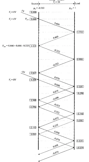
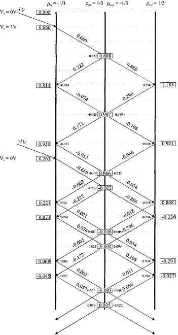
An ideal transmission line is a line through which a signal can be sent without undergoing any attenuation or distortion (Rashid 1990). As a first approximation transmission lines are generally thought of as ideal. This chapter looks at the theory of the ideal transmission line, and how it can be related to microstrip line circuits.
4.1 : Electrical Characteristics of Transmission Lines
4.1.1 : Two-wire transmission line
The end of a two-wire transmission line that is connected to a source is ordinarily called the generator end or the input end. The other end of the line, if connected to a load, is called the load end or the receiving end.
4.1.2 : Equivalent circuit
If given, values of resistance, capacitance, inductance, and conductance in the circuit (figure 4.1) would represent lumped values. It is convenient to analyse one section of the line at a time. To do this adequately, the values should be significant. This type of analysis is valid because at some operating frequency, these values will become highly significant and an integral part of either the output circuit of a stage or part of the input circuit of the next stage (Miller 1983). These values can cause decreased gain, distortion, and undesirable phase shifts (Sinnema 1979). To prevent these undesirable effects, the lumped values may be incorporated into the circuit as usable components, compensated for, or simply tolerated. However, it is important to know their effects to be able to understand the circuits that employ these values as usable components.
In many applications, the values of conductance and resistance are insignificant and may be neglected (Chilo and Amaud 1984). If they are neglected, the circuit will appear as shown in figure 4.2 (Miller 1983). Notice that this network is terminated with a resistance that represents the impedance of the infinite number of sections exactly the same as the section of line under consideration. The termination is considered to be a load connected to the line.
4.1.3 : Characteristic impedance
A line infinitely long can be considered to be composed of an infinite number of inductors and capacitors. If a voltage is applied to the input terminals of the line, current will begin to flow. It will continue to flow as long as the capacitors and inductors were able to assume a charge. Since there are an infinite number of these sections of line, the current will flow indefinitely. If the infinite line were uniform, the impedance of each section will be the same as the impedance offered to the circuit by any other section of line of the same unit length. Therefore, the current would be of some finite value. If the
current flowing in the line and the voltage applied across it are known, the impedance of the infinite line can be determined using Ohm's law. This impedance is called the characteristic impedance, Z0, of the line. If by some means the characteristic impedance of the line were measured at any point on the line away from the ends, it would be found that the characteristic impedance would be the same (Blake 1993) and is also sometimes called the surge impedance.
In figure 4.2 (Miller 1983) the distributed inductance of the line is divided equally into two parts in the horizontal arms of the T. The distributed capacitance is lumped and shown connected in the central leg of the T. The line is terminated in a resistance equal to that of the characteristic impedance of the line as seen across terminals A and B. Since the circuit in figure 4.2 is nothing more than a series-parallel LCR circuit, the impedance of the network may be determined by the formula that will now be developed. The impedance, Z0, looking into terminals AB of figure 4.2 is
Simplifying gives:
<7 . {Z\Z2/2) + Z0Z2
2 + Z2 + (Z,/2) + Z0 (4'2)
Expressing the right-hand side in terms of the lowest common denominator leads to:
Zo = Z,Z2 + (Zf /l)2[Z2 + (Zj/2) + + Z,Z0 + (2ZjZ2/2) + 2Z0Z2 ZQ] (4.3)
result obtained is:
2Z0Z2 + Z0Z, + 2Z0“ — Z,Z2 + (Zf /2) + Z|Z0 + (2ZjZ2/ 2) + 2Z0Zo (^*4)
Simplifying to:
7 2
2Z02 = 2Z,Z2 + (4.5)
or
Z0 — Z,Z2 + ^ 1 (4.6)
If the transmission line is to be accurately represented by an equivalent network, the T- network section of figure 4.2 must be replaced by an infinite number of similar sections (Miller 1983). Thus, the distributed inductance in the line will be divided into n sections, instead of the number (2) as indicated in the last term of equation (4.6). As the number of sections approaches infinity, the last term Z jn will approach zero. Therefore:
Z0 = (4.7)
Since the term Zj represents the inductive reactance and the term Z2 represents the capacitative reactance:
<4-8)
and therefore:
(4.9)
The derivation resulting in equation (4.9) shows that an ideal transmission line's characteristic impedance is dependent upon its inductance and capacitance.
4.2 : Propagation of DC Voltage Along a Transmission Line
4.2.1: Physical explanation of propagation
To better understand the characteristics of a transmission line with an AC voltage applied, the infinitely long transmission line will first be analysed with a DC voltage applied. This will be accomplished using the circuit shown in figure 4.3 (Miller 1983). In this circuit the resistance of the line is not shown, and therefore the line will be assumed to be loss-free; i.e. lossless.
Considering only the capacitor C, and the inductor Lx as a series circuit, when voltage is applied to the network, capacitor C, will have the ability to charge through inductor L v
It is characteristic of an inductor that at the first instant of time when voltage is applied, a maximum voltage is developed across it and minimum current is permitted to flow through it (Duffin 1965). At the same time, the capacitor will have a minimum of voltage across it and a tendency to pass a maximum current (Duffin 1965). The maximum current is not permitted to flow at the first instant because of the action of the inductor, which is in the charge path of the capacitor. At this time the voltage across points c and
value of the applied voltage, capacitor C2 will begin to charge through inductors and
L2. The charging of capacitor C2 will again require time. In fact the time required for the voltage to reach points e and / from points c and d will be the same time as was necessary for the original voltage to reach points c and d. This is true because the line is uniform, and the values of the reactive components are the same throughout its entire length. This action will continue in the same manner until all of the capacitors in the line are charged. Since the number of capacitors in an infinite line is infinite, the time required to charge the entire line would be an infinite amount of time. It is important to note that current is flowing continuously in the line and that it has some finite value.
4.2.2 : Velocity of propagation
When an electromagnetic field is moving down the line, its associated electric and magnetic fields are said to be propagated down the line (Blake 1993). It was found and mentioned previously that time was required to charge each unit section of the line, and if that line were infinitely long, the line would require an infinitely long time to charge. The time for a field to be propagated from one point on a line to another may be computed, for if the time and the length of the line are known, the velocity of propagation may be determined. The network shown in figure 4.4 (Miller 1983) will be used to compute the time required for the voltage wavefront to pass a section of line of specified length. The total charge (0) in coulombs on capacitor C, is determined by the relationship:
Q = CE (4.10)
Since the charge on the capacitor in the line has its source at the battery, the total amount of charge removed from the battery will be equal to:
Q = IT (4.11)
Because these charges are equal, they may be equated thus:
CE = IT (4.12)
As the capacitor C, charges, capacitor C2 contains a zero charge. Since capacitor C,'s voltage is distributed across C2 and Z2, at the same time the charge on C2 is practically zero, the voltage across C, (points c and d) must be, by KirchofFs law, entirely across Lv
The value of the voltage across the inductor is given by:
e = L — ■ (4.13)
At
Since current and time start at zero, the change in time and the change in current are equal to the final current and the final time. Equation (4.13) becomes:
E T = L I (4.14)
Solving the equation for /:
7 = ^ (4.15)
Solving equation (4.12), that was a statement of the equivalency of the charges, for current gives:
/ = — (4.16)
Solving the equation for T:
T2 = LC (4.18)
or
r = VZc
(4.i9)
Since velocity is both a function of time and distance, the formula for computing propagation velocity is:
vp = ^ (4.20)
where V is the velocity of propagation, and D is the distance of travel.
It should again be noted that the time required for a wave to traverse a transmission line segment will depend on the value of L and C and that these values will be different, depending on the type of transmission line considered.
4.3 : Loading of the Line
4.3.1 : Maximum power transfer
Up to this point, only transmission lines that are terminated in a resistive load equal to the characteristic impedance of the line have been considered. This is the ideal case and