Effect of disorder on a graphene
p
-
n
junction
M. M. Fogler,1,*
D. S. Novikov,2,3L. I. Glazman,2,3 and B. I. Shklovskii21Department of Physics, University of California San Diego, 9500 Gilman Drive, La Jolla, California 92093, USA 2W. I. Fine Theoretical Physics Institute, University of Minnesota, Minneapolis, Minnesota 55455, USA
3Department of Physics, Yale University, New Haven, Connecticut 06511, USA 共Received 21 November 2007; published 21 February 2008兲
We propose the theory of transport in a gate-tunable graphenep-njunction, in which the gradient of the carrier density is controlled by the gate voltage. Depending on this gradient and on the density of charged impurities, the junction resistance is dominated by either diffusive or ballistic contribution. We find the con-ditions for observing ballistic transport and show that in existing devices they are satisfied only marginally. We also simulate numerically the trajectories of charge carriers and illustrate challenges in realizing more delicate ballistic effects, such as Veselago lensing.
DOI:10.1103/PhysRevB.77.075420 PACS number共s兲: 81.05.Uw, 73.63.⫺b, 73.40.Lq
I. INTRODUCTION AND MAIN RESULTS
A. Definition of the model
Graphene is a new material whose unique electronic structure endows it with many unusual properties.1A
mono-layer graphene is a gapless two-dimensional semiconductor with a massless electron-hole symmetric spectrum near the corners of the Brillouin zone, ⑀共k兲=⫾បv兩k兩, where v
⬇108cm/s. The concentration of these “Dirac” quasiparti-cles can be accurately controlled by the electric field effect.2,3An exciting experimental development is the ability
to apply such fields locally, by means of submicron gates. Using this technique, graphenep-n junctions 共GPNJs兲 have been recently demonstrated.4–7
Within idealized treatments that neglect disorder and elec-tron interactions, GPNJs were predicted to display a number of intriguing phenomena. They include Klein tunneling,8–10
Veselago lensing,11microwave-induced12,13and Andreev14,15
reflection, as well as strong ballistic magnetoresistance.9,16
Both quantitative and qualitative changes to these phenom-ena are expected when interactions and disorder are included in the model. For example, long-range Coulomb interactions lead to nonlinear screening in GPNJ, which can modify its resistance substantially.17The purpose of this paper is to
in-vestigate how the junction resistance is affected by disorder. We show that in existing GPNJ, this effect is, indeed, strong and we suggest what can be done to reduce it.
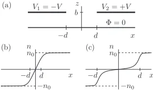
We consider a generic model of an electrostatic GPNJ, in which a grounded graphene sheet in the x-y plane is con-trolled by two coplanar metallic gates with voltagesV1 and V2. The gates are separated by distancebfrom graphene and a distance 2d from each other. Under a symmetric gate bias, V2= −V1=V共Fig.1兲, the graphene carrier densityn共x兲varies linearly in the middle of the junction共x= 0兲,
n共x兲 ⯝n
⬘
x, 兩x兩ⰆD⬅max兵b,d其, 共1兲 and tends to its limiting values⫾n0at兩x兩ⰇD. Here,n⬘
is the density gradient18atx= 0.Our assumptions about disorder require a brief discussion. At present, the nature of disorder in graphene is not com-pletely understood.1 Our knowledge of it derives mainly
from the measurements of the transport mobility . For a
sample with a macroscopically homogeneous carrier concen-trationn and resistivity, the mobility is defined by
共n兲= 1
e兩n兩共n兲. 共2兲
A remarkable fact that holds true for nearly all experiments on graphene is that 共n兲 is observed to be approximately constant away from the charge-neutrality point,n= 0. Rather than entering a debate on the microscopic origin of this be-havior, we adopt it on phenomenological grounds. We can do so because the derivation below applies regardless of the exact microscopic origin of the constant mobility.
It is convenient to define parameter ni of dimension of concentration by
ni= e
h= const, 共3兲
then the resistivity共n兲can be written as
共n兲= h e2
ni
兩n兩, 兩n兩Ⰷni. 共4兲 Below we will also need the carrier mean free pathl, which is related to the conductivity in a standard way:
−1=e 2
h共2kFl兲, 共5兲
wherekF共n兲=
冑
兩n兩is the Fermi wave vector. Using Eq.共4兲, we findl共n兲= kF 2ni
, 兩n兩Ⰷni. 共6兲
The inequality 兩n兩Ⰷni in Eqs. 共4兲 and 共6兲 is stipulated by another phenomenological observation: the saturation of共n兲 at a finite valuemax⬃h/e2 at low carrier densities.1,19
graphene sheet.20,21 An impurity of a unit charge acts as a
scatterer with the transport cross section20–23
⌳= 2c2共␣兲/kF, 共7兲 wherec2=␣2/2 for ␣Ⰶ1 共graphene on large- substrate兲 andc2⬃0.1 for␣⬇1共SiO2substrate兲.24Here,␣=e2/បvis the dimensionless strength of Coulomb interactions and is the effective dielectric constant. If the charged impurities have an average surface concentration Ni, then l= 1/Ni⌳. Comparing this with Eq. 共6兲, one indeed arrives at Eq. 共3兲 with
ni=c2共␣兲Ni. 共8兲
This argument has a considerable appeal and is supported by recent experiments.25
B. Results
To isolate the transport properties specific to GPNJ, we follow the procedure introduced by experimentalists5 and
compute the difference of the total resistanceRtot of the de-vice in thep-n 关Fig.1共a兲兴and then-n states:
R⬅兩Rtot兩V2=−V1=V−兩Rtot兩V2=V1=V. 共9兲
This allows us to largely eliminate the contribution of the bulk regions兩x兩⬎D. Our results are then as follows. We find two qualitatively different regimes, depending on the magni-tude of the dimensionless parameter
= 兩n
⬘
兩 ni3/2. 共10兲
For small  共high disorder or low density gradient兲, the transport is purely diffusive, and the resistance of the GPNJ is given by
Ⰶ1: R⯝2h e2
ni
兩n
⬘
兩Wln共2/3␥兲, 共11兲
whereWis the width of the device in theydirection and␥is defined by
␥⬅ 兩n
⬘
兩1/3DⰇ1. 共12兲 The condition ␥Ⰷ1, which is usually satisfied in experiment,4–7ensures that the densityn共x兲varies across theGPNJ slowly enough, D= max兵d,b其ⰇkF−1共n0兲, to justify its evaluation by means of classical electrostatics.17 Equation
共11兲is written for2/3␥Ⰷ1, i.e., forn0Ⰷni, when the GPNJ is still well defined despite random fluctuations of the elec-tron densityn共x,y兲due to disorder.
In the opposite regime 共large  or low disorder兲, the GPNJ resistance
Ⰷ1: R=Rbal+Rdif 共13a兲 is the sum of the ballistic and the diffusive contributions,
Rbal= h e2
c1
␣1/6兩n
⬘
兩1/3W, c1⬇1.0, 共13b兲Rdif⯝2 h e2
ni
兩n
⬘
兩W ln冉
4␥4/3
冊
, ␥Ⰷ 4/34. 共13c兲 Equations 共11兲 and 共13c兲 are valid with logarithmic accuracy26 and match at ⬃3. The ballistic contribution
dominates,R⯝RbalⰇRdif, provided
Ⰷ*=
冋
2␣ 1/6c1 ln
冉
4␥*4/3
冊
册
3/2. 共14兲
Realistically, the logarithmically “large” threshold
*here is about 10. In recent experiments,5,7 is of the same order of
magnitude. So, they are presumably in the crossover region Rbal⬃Rdif. To move deeper into the ballistic regime, one needs either a larger concentration gradient兩n
⬘
兩 or a higher mobility.The rest of the paper is divided into three sections. In Sec. II, we give the analytical derivation of the above results. In Sec. III, we illustrate them by numerical simulations. Finally, in Sec. IV, we discuss their implications for ongoing experi-mental work.
II. DERIVATION
This section is organized as follows. First, we consider electrostatics of the gate-tunable junction. Next, we study separately the ballistic and the diffusive contributions to the transport. Finally, we combine them to arrive at a total ex-pression for the resistance of a GPNJ.
A. Electrostatics
Electron density in graphene is related to the electrostatic potential ⌽共x,z兲 by the Gauss law, n共x兲=共/4e兲z⌽共x, + 0兲. To find ⌽ and n, we can treat graphene as an ideal conductor. 共For the discussion of this approximation, see Refs. 17 and 27.兲 The calculation can be done using the conformal mapping
2w+ ln
冉
a+w a−w冊
=
b共x+iz兲, 共15兲
which transforms the upper half-planez⬎0 with the branch cuts along the gates关cf. Fig.1共a兲兴to the upper half-plane of a complex variablew=w共x,z兲. Here,a is found from
−d d x
b z
V1=−V V2= +V
Φ = 0 (a)
−d d x n0
n
−n0 (b)
−d d x
n0
n
[image:2.612.95.251.591.683.2]−n0 (c)
冑
a共a+ 1兲+ ln共冑a+冑
a+ 1兲=d/2b. 共16兲 The graphene sheet, the left gate, and the right gate are mapped onto the intervals −a⬍w⬍a, w⬍−a, and w⬎a, respectively, of the real axis. Therefore, the sought potential is given by⌽共x,z兲=共1/兲Im关V1ln共a+w兲−V2ln共a−w兲兴. 共17兲 Using these equations and simple algebra, we find
n共x兲= 8eb
共V2+V1兲a+共V2−V1兲w共x兲
a共a+ 1兲−w2共x兲 , 共18兲 wherew共x兲stands for the real quantityw共x,z= 0兲defined by Eq.共15兲. For the symmetric gate bias, we obtain
n共x兲= n0共V兲w共x兲
a共a+ 1兲−w2共x兲, V2= −V1=V, 共19兲 in which case the density gradient atx= 0 is given by
n
⬘
= 2bn0共V兲
共1 +a兲2, n0共V兲= V
4eb. 共20兲 Two examples ofn共x兲computed according to Eqs.共15兲and 共19兲 are plotted in Figs. 1共b兲 and 1共c兲. In both cases, the linear dependence n⯝n
⬘
x extends up to 兩x兩⬃D. However, for widely separated gates关Fig.1共c兲兴, the local density gra-dient sharply increases near the gate edges. In those regions, n共x兲is dictated by the nearest gate共similar to the case stud-ied in Ref.17兲, and one can show that28max
x
冏
dn dx
冏
⯝
27eb2max兵兩V1兩,兩V2兩其, dⰇb. 共21兲
B. Ballistic resistance
The resistance Rbal of a clean GPNJ is related9 to the
electric field at thep-n interface. To compute this field, one has to go beyond electrostatics of ideal conductors and take into account nonlinear screening at the p-n interface. Equa-tion共13b兲forRbalwas derived from this analysis in Ref.17. In the case ␣⬃1, the result for Rbal can be qualitatively understood as the ballistic resistance of a system with WkF(n共xtun兲)transmitting channels:
Rbal⬃ h e2
1 kFW
⬃ h e2
xtun
W . 共22兲
Here, the effective “width” of thep-n interface
xtun=␣−1/6兩n
⬘
兩−1/3 共23兲is found from the condition that it is of the order of the quantum uncertainty in the quasiparticle coordinate,
xtun⬃kF −1
„n共xtun兲…. 共24兲 共In Ref.17,xtunwas denoted byxTF.兲The quasiparticles that manage to get inside the strip兩x兩⬍xtun cross thep-n bound-ary without tunneling suppression.9
Below we consider the resistance共9兲of a symmetrically biased GPNJ,V2= −V1=V. The transport is either diffusive or ballistic depending on the gradient共10兲.
C. Purely diffusive transport:™1
The derivation is based on treating (n共x兲) as the local x-dependent resistivity. This is justified provided the concen-tration gradient is sufficiently small, such that
l共n兲兩xn兩Ⰶn. 共25兲
Using Eq.共6兲, one can easily check that forⰆ1, the con-dition共25兲is satisfied at all兩x兩Ⰷxflc, wherexflcis defined by
xflc=ni/兩n
⬘
兩, 共26兲see also Fig.2共a兲. At such distances, Eq.共4兲is still valid. On the other hand, in the strip兩x兩ⱗxflc, we have兩n共x兲兩ⱗni, so that Eq. 共4兲 does not apply.29 Since the transport remains
diffusive in the strip兩x兩⬍xflc共certainly, it cannot be ballistic because of strong disorder30兲, we can assume that the
corre-sponding local resistivity is of the order of its bulk value max⬃h/e2 at the charge-neutrality point. This allows us to estimate the resistance of this region as
Rflc⬃max xflc
W . 共27兲
According to our definition 共9兲, the GPNJ resistance is the difference of the total resistances in thep-nandn-n configu-rations. It is convenient to write it asR=Rdif共0兲, where
Rdif共x兲= 2 W
冕
x⬁
dx˜关兩共˜x兲兩V1=−V2−兩共˜x兲兩V1=+V2兴. 共28兲
Using Eqs.共15兲,共19兲, and 共4兲, and the expression
n共x兲= n0共V兲a
a共a+ 1兲−w2共x兲, V1=V2=V, 共29兲 for the charge profile in then-n state that follows from Eq. 共18兲, the integral in Eq.共28兲can be transformed to
Rdif共x兲 ⯝2 h e2
ni
兩n
⬘
兩W ln冋
n0共a+ 1兲兩n
⬘
兩x册
, xⲏxflc. 共30兲 The total resistance is Rdif共xflc兲+Rflc, which leads to Eq. 共11兲. Note that the effect ofRflcis only to modify the numeri-cal factor in the argument of the logarithm in the final ex-pression. For sufficiently long junctions, this logarithm is large关cf. Eq.共11兲兴and so our crude estimate ofRflcis quite acceptable. This can be understood by realizing that in a long junction, the resistance of the兩x兩⬍xflcstrip is much smaller than that of the rest of the system. In shorter devices, thex D
0
0 D x
xflc
xflc xbal
xtun
xtun
β>>1:
[image:3.612.377.496.56.110.2]β<<1:
FIG. 2. A sketch of the characteristic length scales in a GPNJ for the limiting cases of small and large. Only thex⬎0 side of the junction is shown. The diffusive region is hatched. Parametersxtun andxflcare indicated by the dashed lines in the regimesⰆ1 and
contribution of this “fluctuating strip” can be significant, and so a more accurate evaluation of Rdif in Eq. 共28兲 may be necessary. For example, one may want to perform the inte-gration in Eq. 共28兲 numerically using the experimentally measured dependence共n兲 instead of Eq.共4兲.
D. Coexistence of ballistic and diffusive transport:š1
Here, the carrier densityn共x兲varies withxmore rapidly. As a result, the diffusive approximation breaks down inside the strip 兩x兩ⱗxbal, whose width is given by the condition l关n共xbal兲兴⬃xbal, i.e.,
xbal⬃ 兩n
⬘
兩 4ni2. 共31兲
The carrier density atx=xbalis still high,n共xbal兲Ⰷni, so that at兩x兩⬎xbalEq. 共4兲applies. Thus, the diffusive contribution to the resistance isRdif⯝Rdif共xbal兲, leading to Eq.共13c兲.关The extra factor−2under the logarithm in Eq.共13c兲vs Eq.共11兲 comes fromxbal⬃2xflc. Note, however, that xflchas no di-rect physical meaning ifⰇ1.兴
In contrast, within the strip兩x兩⬍xbal, the transport is bal-listic: the local mean free pathl关n共x兲兴nominally exceeds兩x兩, so that quasiparticles reach thep-n interface largely without experiencing impurity scattering. We now note that the tun-neling strip共31兲is located deep inside this ballistic region,
xtun⬃ 4 ␣1/6
xbal
4/3Ⰶxbal, 共32兲 see also Fig. 2共b兲. Therefore, the transmission problem is reduced to the clean case,17yielding Eq.共13b兲for the
ballis-tic resistanceRbal. Due to the large logarithmic factor inRdif 关Eq. 共13c兲兴, the ballistic contribution in Eq. 共13a兲 starts to dominate the diffusive one only whenexceeds a logarith-mically large threshold*关Eq.共14兲兴.
III. NUMERICAL SIMULATIONS
In this section, we illustrate and support the above ana-lytical results by numerical simulations. In particular, we show that the criterionⰇ*关Eq.共14兲兴guarantees only that the total resistance of the junctionRis given by the formula derived for a disorder-free GPNJ关Eq.共13b兲兴. Realization of other ballistic phenomena may demand cleaner systems共see below兲.
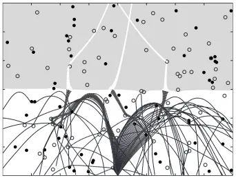
To get intuition above the nature of transport at⬎*, we studied semiclassical trajectories of the quasiparticles in a GPNJ by numerically solving the following relativistic equa-tions of motion:
r˙ =vp/兩p兩, p˙ =ⵜ兩⌽共r兲兩. 共33兲 For illustrative purposes, we adopted the potential
⌽共r兲= − sgn共x兲
冑
n⬘
兩x兩+兺
jQj
冑
共r−rj兲2+zj2. 共34兲
Here, the first term models the potential induced by the gates17 and the second term represents the potential created
by impurity charges Qj=⫾1 with coordinates 共rj,zj兲. This expression assumes␣=e2/=ប=v= 1 and neglects, for sim-plicity, the screening of these impurities by the electrons in graphene. We estimate that this entailsc2⬃1 in Eq.共8兲.
Other parameters of the simulation were as follows. Thez coordinates of all the impurities were set tozj= 0.01 in some arbitrary length units. The in-plane coordinates of the impu-rities were chosen randomly inside the square 兩x兩,兩y兩⬍100 straddling the p-n interface. The total impurity number was 300, so thatni⬃300/2002= 0.0075. In the field of view 兩x兩
艋60,兩y兩艋80 of Fig.3, 126 of these impurities are seen. The density gradient was set to ben
⬘
= 0.25, which makes param-eter quite large:= 0.25/ni3/2⬃400.In Fig.3, we show 51 electron trajectories computed by standard numerical algorithms.31The energy for all
trajecto-ries was fixed at zero and the starting point was set to x=x0= −60, y= 0. The polar angles of the initial velocities formed an equidistant set spanning the interval 共−/5 ,/5兲.
From Eq.共31兲, we estimatexbal⬃350. Therefore, the in-jection point is deep inside the ballistic strip,x0Ⰶxbal. Simul-taneously,x0Ⰷxtun⬇2 关cf. Eq.共23兲兴, so that the semiclassi-cal approximation共33兲is legitimate.
As evident from Fig.3, the average distance between col-lisions of quasiparticles with impurities exceeds the distance x0 from the injection point to the interface. Thus, in agree-ment with the above estimates, electrons can propagate across the interface according to the formulas derived for the disorder-free system.9,17A closely related observation is that
for the chosen parameters, there are many points along the interface not “blocked” by the impurities.
On the other hand, even for such large , there is no evidence for the recently proposed11Veselago lensing effect:
[image:4.612.352.523.56.185.2]electrons can penetrate through the p-n interface: the trans-verse momenta of such electrons must satisfy the condition9,17
兩py兩ⱗ
ប xtun
. 共35兲
Such momenta are much smaller than the typical ones,
py⬃ប
冑
n⬘
x0⬃冉
ប xtun冊
冑
x0 xtun
. 共36兲
Furthermore, scattering of an electron by a Coulomb impu-rity typically deflects the electron trajectory by a substantial angle. Therefore, the lensing additionally requires that a nar-row fan of trajectories defined by Eq.共35兲does not undergo impurity scattering. The width of this fan in real space is ⬃
冑x
0xtun. Therefore, the condition onx0 becomesnix0
冑
x0xtunⱗ1. 共37兲Accordingly, the injection and collection contacts must be placed no further than the distance
xlens⬃ 1 ni2/3xtun1/3
⬃ 4
8/9xbal 共38兲 from the interface, which may be considerably smaller than xbal. Indeed, the absence of a discernible Veselago lensing in Fig.3 is in agreement with our estimates: since x0= 60 and xlens⬃20 关cf. Eq. 共38兲兴, we are not yet in the regime x0 Ⰶxlens.
IV. DISCUSSION AND CONCLUSIONS
In this final section, we discuss geometrical requirements imposed by the criterion共14兲in actual experiments. Using a realistic number ⬃2500 cm2/共V s兲 in Eq. 共3兲, we get ni
⬃1.0⫻1011cm−2. Suchn
i can be achieved if the transport mobility is limited by, e.g., charged impurities of concentra-tionNi⬃1012cm−2 关assumingc2⬃0.1 in Eq.共8兲兴.
We consider first the case of a narrow gap between the gates, b⬇d 关Fig. 1共b兲兴, where a⬇0.4. Taking ␣⬃1, b ⬇50 nm, andn0⬃2⫻1012cm−2, similar to those of Ref.5, for the aboveni, we get⬃10. Some evidence for the bal-listic transport was indeed seen under such conditions.5 On
the other hand, observing Veselago lensing11 seems rather
challenging: it requires placing the injection and collection
contacts within⬃10 nm from each other,关cf. Eq.共38兲兴. Next, in the case of widely separated gates,d= 1m共and the same b= 50 nm兲, we get ⬇0.1 even for a very high maximum densityn0= 1013cm−2. In order to observe ballistic transport in this device, the suggested setup should be some-what modified. For example, using a backgate, one can in-troduce a uniform offset of the electron densityn共x兲, which would shift the location of thep-n interface away from the x= 0 point and closer to the edge of either one of the gates, as discussed in Ref.17. In this manner, the density gradientn
⬘
at the GPNJ can be ramped up to its maximum value共21兲, yieldingsimilar to that in a narrow-gap device.Although we considered a particular junction geometry 关Fig.1共a兲兴our treatment can be readily extended to charac-terize transmission in any GPNJ with a smoothly varying electron density,␥Ⰷ1. The basic steps are as follows:共i兲find the carrier density gradientn
⬘
at thep-n interface,共ii兲 com-putefrom Eq.共10兲,共iii兲determine, based on the criterion 共14兲whether the device is diffusive or ballistic, and finally, 共iv兲 find the diffusive and ballistic contributions from Eqs. 共11兲,共12兲,共13a兲, and共13b兲.关Formula forRdifcan be further refined if the integration in Eq. 共28兲 is done numerically using an accurately measured density dependence of the bulk resistivity共n兲.兴To conclude, disorder can strongly inhibit the ballistic transport regime in graphene field-effect devices. In recent experiments4–7 on graphene p-n junctions, this regime was
reached only marginally at best. For ballistic devices, one should aim at larger electron density gradientsn
⬘
and higher mobilities to satisfy the condition共14兲. Note that if the pri-mary source of disorder are charged impurities, then the re-quirement onn⬘
becomes less stringent for substrates of high dielectric constant . In this case, on the one hand, n⬘
is larger for the same gate voltage and, on the other hand, the influence of Coulomb scattering is smaller,c2⬀␣2⬀−2.ACKNOWLEDGMENTS
This work is supported by NSF Grants Nos. DMR-0706654, DMR-0749220, and DMR-0754613. We are grate-ful to D. Goldhaber-Gordon, B. Huard, and L. M. Zhang for comments on the manuscript. M.F. thanks the W. I. Fine TPI for hospitality and L. M. Zhang for help with computer simulations.
1A. K. Geim and K. S. Novoselov, Nat. Mater. 6, 183共2007兲; A.
H. Castro Neto, F. Guinea, N. M. R. Peres, K. S. Novoselov, and A. K. Geim, arXiv:0709.1163共unpublished兲.
2K. S. Novoselov, A. K. Geim, S. V. Morozov, D. Jiang, Y. Zhang,
S. V. Dubonos, I. V. Grigorieva, and A. A. Firsov, Science 306, 666共2004兲.
3K. S. Novoselov, A. K. Geim, S. V. Morozov, D. Jiang, M. I.
Katsnelson, I. V. Grigorieva, S. V. Dubonos, and A. A. Firsov,
Nature共London兲 438, 197共2005兲.
4M. C. Lemme, T. J. Echtermeyer, M. Baus, and H. Kurz, IEEE
Electron Device Lett. 28, 283共2007兲.
5B. Huard, J. A. Sulpizio, N. Stander, K. Todd, B. Yang, and D.
Goldhaber-Gordon, Phys. Rev. Lett. 98, 236803共2007兲. 6B. Özyilmaz, P. Jarillo-Herrero, D. Efetov, D. A. Abanin, L. S.
Levitov, and P. Kim, Phys. Rev. Lett. 99, 166804共2007兲. 7J. R. Williams, L. DiCarlo, and C. M. Marcus, Science 317, 638
8M. I. Katsnelson, K. S. Novoselov, and A. K. Geim, Nat. Phys. 2,
620共2006兲.
9V. V. Cheianov and V. I. Fal’ko, Phys. Rev. B 74, 041403共R兲 共2006兲.
10J. M. Pereira, Jr., V. Mlinar, F. M. Peeters, and P. Vasilopoulos,
Phys. Rev. B 74, 045424共2006兲.
11V. V. Cheianov, V. I. Fal’ko, and B. L. Altshuler, Science 315,
1252共2007兲.
12B. Trauzettel, Ya. M. Blanter, and A. F. Morpurgo, Phys. Rev. B
75, 035305共2007兲.
13M. V. Fistul and K. B. Efetov, Phys. Rev. Lett. 98, 256803 共2007兲.
14C. W. J. Beenakker, Phys. Rev. Lett. 97, 067007共2006兲. 15A. Ossipov, M. Titov, and C. W. J. Beenakker, Phys. Rev. B 75,
241401共R兲 共2007兲.
16A. V. Shytov, N. Gu, and L. S. Levitov, arXiv:0708.3081共
unpub-lished兲.
17L. M. Zhang and M. M. Fogler, arXiv:0708.0892共unpublished兲. 18Note thatn⬘stands for the density gradient computed classically.
Quantum effects decrease共Ref.17兲truen⬘.
19Y.-W. Tan, Y. Zhang, K. Bolotin, Y. Zhao, S. Adam, E. H. Hwang,
S. Das Sarma, H. L. Stormer, and P. Kim, Phys. Rev. Lett. 99, 246803共2007兲.
20T. Ando, J. Phys. Soc. Jpn. 75, 074716共2006兲.
21K. Nomura and A. H. MacDonald, Phys. Rev. Lett. 98, 076602 共2007兲.
22E. H. Hwang, S. Adam, and S. Das Sarma, Phys. Rev. Lett. 98,
186806共2007兲.
23D. S. Novikov, Phys. Rev. B 76, 245435 共2007兲; Appl. Phys.
Lett. 91, 102102共2007兲.
24Treating the impurity screening within the random phase
approxi-mation共RPA兲and calculating the scattering cross section pertur-batively yields共Refs.20and22兲 c2共0.9兲⬇0.05. For␣⬃1, this calculation is likely to underestimatec2. Using the RPA at the Dirac point and treating scattering off the resultant Coulomb potential exactly gives共Ref.23兲c2共0.9兲⬇0.26共when averaged over the donors and acceptors兲. This is likely to overestimate the resistivity. Thus, the truec2共␣⬃1兲is probably close to 0.1. 25J. H. Chen, C. Jang, M. S. Fuhrer, E. D. Williams, and M.
Ishi-gami, arXiv:0708.2408共unpublished兲; see also Ref.19. 26However, we choose to keep the numerical factor 4in the
ar-gument of the logarithm in Eq.共13c兲because it can be signifi-cant in practice.
27See M. M. Fogler, D. S. Novikov, and B. I. Shklovskii, Phys.
Rev. B 76, 233402共2007兲, and references therein. 28This follows from Eq.共4兲of Zhang and Fogler共Ref.17兲. 29The subscript “flc” inx
flcstands for “fluctuation” to express the idea that inside the strip兩x兩⬍xflc, the local electron concentra-tion presumably exhibits spatial fluctuaconcentra-tions of amplitude ⬃ni
due to disorder, which overwhelm the average linear trend of Eq. 共1兲.
30In addition, we assume that the temperature is not too low and
neglect any localization effects.