Hewlett·Packard Company Roseville Networ~ Division 8000 Foothills Boulevard Roseville, California 95678
HP 9000 Series 800 Computers
HP27114B
Asynchronous FIFO Interface
Reference Manual
FliDW
HEWLETT
~~
PACKARD
Printing History
New editions are complete revisions of the manual. Update packages, which are issued between editions, contain additional and replacement pages to be merged into the manual by the customer. The dates on the title page change only when a new edition or a new update is published. No information is incorporated into a reprinting unless it appears as a prior update; the edition does not change when an update is incorporated. Many product updates do not require manual changes and, conversely, manual corrections may be done without accompanying product changes. Therefore, do not expect a one-to-one correspondence between product updates and manual updates.
Edition 1 . . . September 1989
Notice
Contents
Chapter 1
General Information
Description . . . 1-2 Replacement Manuals . . . 1-2 Equipment Supplied . . • . . . • . . . 1-3 Options . . . • . . . 1-3 Other Recommended Equipment . . . 1-3 Identifying the API . . . 1-4 System Requirements . . . 1-4 System ConftgUl'ation . . . 1-5
Chapter 2
Configuration and Installation
Protecting the API Against ESD . . . 2-1 Unpacking the API . . . 2-2 Default Configuration . . . 2-2 Factory Jumper Settings . . . 2-2 Reset Default Conditions . . . 2-3 Choosing the Mode for the External Device . . . 2-5 Single-Ended Configurations . . . 2-5 Single-Ended, High-True Logic Applications . . . 2-7 Mode Jumper Installation . . . . . 2-7 High-True Resistor Networks . . . 2-7 Single-Ended, Low-True Logic Applications . . . 2-9 Mode Jumper Installation . . . 2-9 Low- True Resistor Networks . . . 2-9 Differential ConftgUl'ations . . . 2-11 Mode Jumper Installation . . . 2-11 Line Termination Resistor Networks . . . 2-11 Handshake Timing Control Jumpers . . . . 2-12 PCTL Pulse Delay/Extension . . . . 2-13 PFLG Filtering . . . . 2-14 Cables . . . " . . . 2-15 Custom Length Cables . . . 2-15 Single-Ended Cables . . . 2-16 Differential Cables . . . 2-16 Wiring the Custom API Cable . . . . 2-17 Planning the API Cable . . . . 2-17 Constructing the Cable . . . 2-18
Chapter 2
Configuration and Installation (cont'd)
Installing the API . . . . 2-22 Selecting a Slot . . . . 2-22 Orienting the PCA . . . • . . . . 2-22 Inserting the PCA . . • . . . 2-23 Connecting the Cable • . . • . . . . . 2-23 Startup and Verification .. . . . . 2-24 Applying Power to the PCA . . . 2-24 Configuring the Operating System . . . . 2-24 Testing the API . . . • . . . 2-24 Connecting the Peripheral Device . . . 2-25 Grounding the Cable • . • . . . '. . . . 2-25 Wiring the Peripheral Device . . . . 2-27 I..ogic Sense . . . • . . . . • . . . . 2-29
Chapter 3
Theory of Operation
Chapter 3
Theory of Operation (cont'd)
Midplane Circuitry (cont'd)Register Operation . . . 3-22 Interrupt Handling . . . 3-22 Backplane Interface Circuitry . . . . 3-23 Backplane Data Transfer . . . . 3-23 Output Transfers . . . • . . . 3-23 Input Transfers . . . 3-23 Handshake Control State Machine . . . . 3-24 Frontplane Handshaking . • . . . . . . . 3-24 FIFO Handshaking Mode . . . 3-26 Full Master Handshake Output . . . . 3-28 Full Slave Input Handshake . . . . . . . 3-29 Full Master Input Handshake . . . • . . . . 3-30 Full Slave Output Handshake . . . . 3-31 Backplane Handshaking . . . 3-32
Chapter 4
Application Design
Transfers through the Backplane . . . . . . .4-2 Output Transfers . . . .4-2 Input transfers . . . 4-2 Application Planning . . . .4-3 Writing the Application . . . 4-3
Chapter 5
Hardware Troubleshooting
Field Replaceable Units . . . . . . ... . . 5-1 Troubleshooting Strategy . . . 5-2 Maintenance Aids . . . 5-2 AFI Device Adapter Diagnostic . . . 5-3 Removing the AFI . . . 5-5 Reshipping the AFI . . . 5-5
Appendix A
Connector and Cables
Frontplane Connector . . . A-1
Differential Signal Cable Assignments . . . . A-2
Single-Ended, High-True Signal Cable Assignments . . . A-4
Single-Ended, Low-True Signal Cable Assignments . . . A-6
Cable Pin Assignments for Cable 27114-63001 . . . . A-8
Alternative Termination of Cable . . . A-9
Appendix B
Product History
Upgrading to the HP 27114B . . . B-1
Appendix C
Error Messages
Error Messages . . . • . . . C-l
Appendix D
Schematics
Address Decoder PAL . . . • . . . D-2 Timing Extension PAL . . . D-4 FIFO PAL . . . • • . . . D-6 Interrupt Control PAL . . . • . . . D-IO
Figures
Chapter 1
General Information
Figure 1-1. The API Identification Stickers . . . . . . .. 1-4 Figure 1-2. API in a Typical Hewlett-Packard System . . . 1-5
Chapter 2
Configuration and Installation
Figure 2-1. Locations of Configuration Jumpers . . . 2-4 . Figure 2-2. Single-Ended, High-True Configuration . . . 2-6 Figure 2-3. Installing the High-True Resistor Network SIPs . . . 2-6 Figure 2-4. Driver/Receiver Grounding in Single-Ended,
High-True Mode . . . 2-7 Figure 2-5. Single-Ended, Low-True Configuration . . . 2-8 Figure 2-6. Installing the Low-True Resistor Network SIPs . . . 2-8 Figure 2-7. Driver/Receiver Grounding in Single-Ended,
Low-True Mode . . . 2-9 Figure 2-8. Differential Mode Configuration . . . . 2-10 Figure 2-9. Installing the Differential Resistor Network DIPs . . . 2-10 Figure 2-10. Driver/Receiver Connection in Differential Mode . . . . 2-10 Figure 2-11. Output Control Jumpers . . . 2-12 Figure 2-12. Example of a Pulse Length Delay/ Extension . . . . 2-13 Figure 2-13. Example of Window Rejecting PFLG Signal . . . . 2-14 Ftgure 2-14. Filling in the API Cabling Worksheet . . . 2-17 Figure 2-15. Wiring the Custom API Cable . . . 2-18 Figure 2-16. A Typical API Installation . . . 2-23 Figure 2-17. A Cable Grounding Bracket . . . 2-26 Figure 2-18. The Wire-Wrap Pinout Orientation . . . 2-27 Figure 2-19. The Wire-Wrap Adapter as the External Device
Connector . . . 2-28 Figure 2-20. The Wire-Wrap Adapter in an Intermediate Cable . . . 2-28 Figure 2-21. Differential Wiring for External Device Connector . . . 2-29 Figure 2-22. Single-Ended Cabling to External Device . . . . 2-29
Chapter 3
Theory of Operation
Figure 3-1. The API Planes • • . • . . . . . . 3-1 Figure 3-2. Transfer Counter Operation . . . 3-21 Figure 3-3. API Registers on the Data Bus . . . 3-22 Figure 3-4. API Interrupt Circuitry . . . . 3-22 Figure 3-5. Output FIFO Handshake . . . 3-26 Figure 3-6. Input FIFO Handshake . . . . 3-27 Figure 3-7. Output Full Master Handshake . . . . 3-28 Figure 3-8. Input Full Slave Handshake . . . 3-29 Figure 3-9. Input Full Master Handshake . . . . 3-30 Figure 3-10. Output Full Slave Handshake . . . 3-31 Figure 3-11. FIFO Buffer Signals IR and OR . . . . 3-32
Appendix D
PAL Equations and Schematics
Tables
Chapter 1
General Information
Table 1-1. HP 27114B API Specifications . . . 1-6 Table 1-2. External Device Driver and Receiver Requirements . . .. 1-6 Table 1-3. Factory Configuration . . . 1-7
Chapter 2
Configuration and Installation
Table 2-1. Factory Configuration . . . 2-2 Table 2-2. Default Configuration . . . 2-3 Table 2-3. PerL Pulse Extension Jumpers . . . 2-13 Table 2-4. PFLG Filtering Jumpers . . . 2-14 Table 2-5. API Cabling Worksheet . . . . 2-19
Chapter 3
Theory of Operation
Table 3-1. Program Domain to API Hardware Domain Conversion . 3-2 Table 3-2. Register Access Address Decoding . . . 3-9 Table 3-3. FIFO Buffer Status as Shown by AEF and HF . . . 3-14 Table 3-4. Mode Bit Patterns . . . . 3-18
Chapter 4
Application Design
Table 4-1. Device Requirements Table . . . 4-3
Appendix A
Connector and Cables
Table A-1. API Frontplane Connector (J2) Pin Assignments . . . A-1
Table A-2. API Cable (27114-63001) Signal Locations
(Differential Mode) . . . A-2
Table A-3. API Cable (27114-63001) Signal Locations
(Single-Ended, High-True) . . . A-4
Table A-4. API Cable (27114-63001) Signal Locations
(Single-Ended, Low True) . . . A-6
Table A-5. API Cable (27114-63001) Wiring Assignments . . . A-8
Table A-6. Conductor Assignment for Cable 27114-63001 . . . A-9
1
I
Note
I
General Information
The Hewlett-Packard Asynchronous FIFO Interface (API) device adapter (interface card) fits all HP Precision Architecture Computers using the Channel I/O Bus (Cm). This chapter gives general information about the API, its requirements and specifications, and what you need to make it work. Specific information follows in subsequent chapters and appendixes. Throughout the manual, all part numbers (in parentheses) refer to
Hewlett-Packard part numbers, unless noted otherwise.
The API is a very versatile I/O device adapter. In order to make it function, you must understand your application, the external (peripheral) device, and the API device adapter. Chapter 3, Theory of Operation, contains the material you need to know to understand the API. Chapter 4, Application Design, tells you how to plan an application. Please read both
of these chapters before trying to program the API or design a new exter-nal device.
This manual is intended for Hewlett-Packard Customer Engineers (CEs), HP Systems Engineers (SEs) and customers. Some of the material presented is inappropriate to some of these groups, and requires specialized training offered by Hewlett-Packard Company. If you do not understand a topic, check to be sure the subject matter covered is not identified as needing such training. If it is, contact HP for assistance before proceeding.
Description
Replacement Manuals
The API has five key components:
• The printed circuit assembly (PCA) (part number 2711460101) -When shipped from the factory, the PCA is configured for differential mode. Therefore, only resistor networks for differential mode are included.
• The connecting cable (part number 27114-63001) - works either in a differential or a single-ended application. The cable component also includes a 96-pin, male, wire wrap adapter (part number 1252-1643) used for the peripheral connector or as the connector for an extension cable.
• The reference manual kit (part number 27114-92001) - which contains this manual (theAsynchronous FIFO Interface Reference Manual) (part number 27114-90004), the Asynchronous FIFO Interface Programmer's Guide (part number 27114-90003), the Asynchronous FIFO Interface Application Notes (part number 5958-9044) and the Asynchronous FIFO Interface Performance Brief (part number 5958-9045).
• The software driver (gpioO) - part of the HP-UX Fundamental Operating System included with your computer.
• The application software (which you supply).
For an API application to function, you must have each of these parts. Hewlett-Packard Company does not supply the application software, but the reference manuals explain how to write one. If you will be using the Hewlett-Packard Device I/O Library (OIL), you should also have avail-able the Device I/O and User Interfacing (part number 97089-90054) manual from the HP 9000 Programmer Series: Concepts and Tutorials.
The manuals shipped with your API come as a single unit. However, to order replacement manuals, you need to order the contents individually.
Equipment Supplied
Options
Option #OBO: 'Option #002: Option #003:
Option #004:
Option #005:
Other Recommended
Equipment
Of the five components, three are included with the API product: • The peA (27114-60101).
• The connecting cable (27114-63001) and wire wrap adapter (1252-1643).
• The reference manual kit (27114-92001).
Hewlett-Packard offers many options to adapt the features of the API to your needs. The options are:
Deletes the manual kit (part number 27114-92001). Adds the loopback test hood (part number 27114-60002). Single-ended option.
Adds three reference SIP resistor networks (part number 1810-0906) and three load SIP resistor networks (part number 1810-0677).
12-meter cable option.
Deletes the 3-meter, 96-conductor cable (part number 27114-63001). Adds a 12-meter, 96-conductor cable (part number 27114-63003). Deletes the 3-meter, 96-conductor cable (part number 27114-63001).
You need the loopback hood (part number 27114-60002) to run the API diagnostic tests included with the HP-UX Fundamental Operating System. If you ordered option #002, you already have a loopback test hood.
Identifying the
AFI
Every product Hewlett-Packard makes has a product number (such as HP 27114B), and each component of the product has a part number. You can identify the API PCA by locating the two paper stickers attached to the fiberglass board. They will look like this:
27114-66666
21
2823A56789
DIY
A-4321
52A654321
MADE IN U.S.A.
52
System
Requirements
Figure 1·1. The AFI Identification Stickers
The information on the stickers will help HP give you faster help if you need it. Copy these identification numbers to a convenient location, such as your log book, where they will be available when you call.
For the API to operate properly, the host computer system must meet certain requirements.
• The computer must be a Hewlett-Packard 9000 series 800 computer with the CIO backplane. Use of the HP 27114B API card in any other computer will not work.
System Configuration
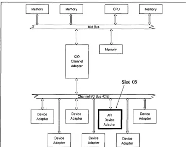
Figure 1-2 is a block diagram showing a typical HP computer system with an AFI installed.CIO
Channel Adapter
Device Adapter
[image:15.615.168.547.129.427.2]Slot 05
Figure 1-2. AFI in a Typical Hewlett-Packard System
You must place the AFI in the lowest group of the card cage slots (slots 0--7). The default slot is 5. Lower numbered slots have priority over higher numbered slots. Refer to the System Administrator's Manual for information on configuring the AFI device adapter into your computer system.
Features
Cable Specification (27114-63001)
Electrical and Cooling Requirements
Peripheral Line Driver
[image:16.615.64.552.67.572.2]Peripheral Receiver
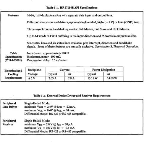
Table 1-1. HP 27114B AFI Specifications
16-bit, half-duplex transfers with separate data input and output lines.
Differential receivers and drivers; optional single-ended, high- (
+
5 V) or low- (GND) true. Three asynchronous handshaking modes: Full Master, Full Slave and FIFO Master.Up to 64 words of FIFO buffering in the input direction and 55 words in output transfers. Six control lines and six status lines available, plus interrupt, direction and handshake signals. Some of these features are mutually exclusive. See chapter 3, Theory of Operation. Impedance: approximately 120 O.
Resistance/meter: 190 mO. Propagation delay: 5.5 ns/meter.
Backplane Voltage
+5V
typical 2.63 A
Current
20
2.8 A
Power Dissipation
typical 20
13.15W 14.00W
Table 1-2. External Device Driver and Receiver Requirements
Single-Ended Mode:
minimum VOH
=
2.4V @ IOH=
-2.6mA. maximum VOL=
O.4V @ IOL=
24 mAoDifferential Mode: RS-422 or RS-485 compatible. Single-Ended Mode:
minimum VIH
=
2.0 V @ bH=
20 !lAomaximum VIL
=
0.8 V @ bL=
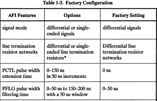
-0.4 mAoTable 1-3. Factory Configuration
AFI Features Options Factory Setting
signal mode differential or single- differential signals
ended signals
line termination differential or single- Differential line resistor networks ended line termination termination resistor
resistors· networks
perL pulse width 0--150 ns Ons
extension time in 50 ns increments
PFLG pulse width 0--50 ns to 150--200 ns 0--50 ns
filtering time with a 50 ns window
• DIP line termination resistor networks are used for differential signals. SIP line termination resistor networks are used for single-ended signals.
2
Protecting the
AFI Against ESD
I
Caution
I
Configuration and
Installation
This chapter contains the following information for the HP 27114B Asynchronous FIFO Interface (AFI) device adapter:
• Protecting the AFI against electrostatic discharge. • Unpacking and inspection.
• Factory configuration.
• Configuration jumper placement. • Cabling information, including pinouts. • Installing the PCA and cable.
• Connecting the external device. • Start-up and verification.
Some of the components used in this product are susceptible to damage by electrostatic discharge (ESD). Refer to the safety information at the front of your host system manual before handling the AFI printed circuit assembly (PCA). The PCA is shipped in a static-shielding bag. Leave it in the bag until you install it in the computer system. When handling the PCA outside of this container, do not touch any components. Hold the peA by its edges, avoid working in a carpeted area, use a grounding wrist strap, reduce unnecessary movements; all of these precautions will reduce the chances of ESD damage.
ESD can destroy any electronic assembly. Failure to follow anti-ESD procedures can invalidate your warranty.
Ideally, while you are configuring the device adapter for your application, you will have a special anti-ESD work area set aside. If you do not, we suggest using a work station kit like the one provided with part number 9300-1155. It contains a grounding wrist strap, a conductive work mat and other items to shunt any charge safely to ground. Instructions for use come with the kit.
Unpacking the
AFI
Default
Configuration
Factory Jumper
Settings
Carefully examine the condition of the box and other packaging material.
If you discover any damage, stop. Call your HP Sales and Support Office. Have the carrier's agent present to ensure that your claim will be upheld in case of damage. The Sales and Support Office will help with these details. Keep the packaging material for later use.
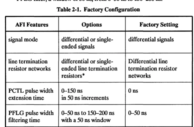
Table 2-1 shows the physical settings on the PCA as shipped by the factory. Table 2-2 shows the API default configuration on power-up.
The API has several options selected using jumpers. See table 2-1. These options are:
• Differential or single-ended mode.
[image:20.613.219.547.359.573.2]• Length of PCTL pulse extension, from 0 to 150 ns in 50 ns increments. • PFLG filter, a window of 50 ns, from 0-50 ns to 150-200 ns.
Table 2-1. Factory Configuration
AFI Features Options Factory Setting
signal mode differential or single- differential signals ended signals
line termination differential or single- Differential line resistor networks ended line termination termination resistor
resistors
*
networksPCTL pulse width 0-150 ns Ons
extension time in 50 ns increments
PFLG pulse width 0-50 ns to 150-200 ns 0-50 ns filtering time with a 50 ns window
*
DIP line termination resistor networks are used for differential signals. SIP line termination resistor networks are used for single-ended signals. During the assembly of the device adapter, Hewlett-Packard inserts the jumpers for these choices:Reset Default
Conditions
To choose an alternative setting, remove the appropriate jumper and place it in another position. This chapter explains these procedures in each configuration section.
After recovering from any reset condition, including the initial state after switching the computer on, the API device adapter takes on certain characteristics defmed by its software driver defaults. See table 2-2.
Table 2-2. DeCault Configuration Driver Selected Parameter Reset DeCault
Transfer counter disabled
PEND option disabled
ATIN interrupt enabled
REND/CTIA REND selected (CTIA ignored)
ATIN/STS5 ATIN selected (STS5 ignored)
PDIR/CTLS PDIR selected (CTLS ignored)
PEND/STS4 STS4 selected (PEND ignored)
The defaults are:
• Transfer counter is disabled.
• ATIN (attention) interrupt is enabled. • PEND (peripheral end) is disabled. • Output control lines selected:
• REND (host end) is selected over CTIA.
• ATIN (attention) is selected over STS5.
• PDIR (transfer direction) is selected over CTL5. • STS4 is selected over PEND (peripheral end).
To choose any of the options, your application program must explicitly override these default settings. The Asynchronous FIFO Interface Programmer's Guide (part number 27114-90003) explains this process.
o
J1
Mode Selection Jumpers
~ 000000000000000000000000000000000000000000000000 ~ ~ 000000000000000000000000000000000000000000000000 ~ ? 000000000000000000000000000000000000000000000000
Gl 000000000000000000000000000000000000000000000000
~ 000000000000000000000000000000000000000000000000 i
Z
000000000000000000000000000000000000000000000000 ~~
~:stor
network socket
P1
~
U74 Resistor networksocket
~
U104 !i Resistor network socket
Crystal
~~U
OSocillator JumpersU
o
Figure 2-1. Locations of Configuration Jumpers
I
Note
I
Figure 2-1 shows the PCA with the component side facing you and the frontplane connector, J1, uppermost. The most noticeable component is the mode jumper block, near the connector. On the PCA, it has 12 jumpers (not shown here) installed. Below the jumper block are the three resistor network sockets with DIP networks (not included in this illustra-tion) installed. In the lower right corner, near the crystal oscillator, is the jumper block for the PFLG and PCfL timing controls.
Choosing the
Mode
for the
External Device
I
Note
I
Single-Ended
Configurations
I
Note
I
The API allows for either differential ("balanced") or single-ended ("un-balanced") external devices. Differential devices have distinct advantages in terms of usefulness. The choice of a single-ended peripheral device
imposes some limitations on your application. The principal ones are: • Restricted cable length.
• Increased noise susceptibility.
The other design concern is logic sense, either low- or high-true. The API supports both, but there are advantages to using a low-true device.
If you do not understand CIO logic inversion, read "Logic Sense" later in this chapter. Terminology used here refers to the API hardware logic, not to what a user sees from the host computer.
Of the three configuration sections (two single-ended, one differential) that follow, you need to read only the one that applies to your application.
Because of the limitations of single-ended data transfers, Hewlett-Packard suggests you design a differential peripheral device if you have the choice. However, the API device adapter supports single-ended applications in either high-true or low-true mode. Here, we explain how to configure the API for single-ended mode, both for high-true and low-true logic. You need to read only the section that applies to your configuration needs. To use a single-ended peripheral,
• Move the mode selection jumpers from the factory setting (differen-tial mode) to the correct locations for your application.
• Remove the differential termination resistor networks and install the termination resistor networks for single-ended applications.
Figure 2-2 shows the jumper block with the jumpers in the single-ended, high-true positions. Figure 2-5 shows a low-true application.
The networks have a printed pin 1 designator, a dot or vertical bar. Molded dots on the case have no meaning. Do not confuse these marks.
Load all three resistor
networks sockets the same. Load SIP goes on right, reference SIP on left. SIP pin 1 goes socket pin 1 or 20. in Figure 2-2. Single-Ended, High-True Configuration
Front Pin 1 symbol
may be dot or vertical bar
11 0
12 0
13 0 0 0 0 Reference 14 15
Network 16
(1810-0906) 17 0
18 0
19 0
•
20 00 0 0 0 0 0 0 0 0 0
~
10
9
8 7
6 5
4 3
2
Rear Molded dots on SIP case have no meaning
Load Network (1810-0677)
Single-Ended,
High-True Logic
Applications
I
Caution
I
Mode Jumper Installation
In a high-true logic application, move six of the mode jumpers and replace the DIP termination resistor networks with SIP termination resistor net-works.
ESD can destroy any electronic assembly. Failure to follow anti-ESD procedures can invalidate your warranty.
There are two blocks of jumper pins. The upper block (W707) is labeled
G
J
C-
on the left end; the lower (W606) labels areG
J
C
+.
To use a single-ended, high-true application, remove all six of the jumpers from the upper jumper blocks (nearer the frontplane connector). Then place them as shown in figure 2-2. The jumpers on the upper blocks will now connect the pins in row J to row G. Those on the lower blocks will remain connect-ing the jumper pins from row J to the pins in row C+ .
By moving the jumpers on the upper blocks, the signals coming from the frontplane connector to the pins in row J are grounded to row G. This permits single-ended high-true use.
The pins in row C
+
are the leads from the (+ )
side of the API drivers or receivers. Pins in row J go to the frontplane cable connector. By shorting these pins, the output signals from the (+ )
side of the drivers go to the connector, and the input signals from the peripheral will go to the (+) side of the receivers. This is the factory setting for the lower jumpers.r----~ To frontplane 220 0
3300
C+ J G
C-
J G
1.SkO
L--_~ To frontplane From
frontplane
Figure 2-4. Driver/Receiver Grounding in Single-Ended, High-True Mode
High-True Resistor
Networks
The API drivers and receivers must have resistor networks installed in the three 2O-pin sockets shown in figure 2-2. Figure 2-3 shows the orientation for the single, in-line packages (SIP) for high-true applications. Position the taller "load" SIP (part number 1810-0677) with its pin 1 in pin 1 of each socket. Place pin 1 of the "reference" SIP (part number 1810-0906) into socket pin 20. Identify pin 1 on the SIP by the printed symbol, either a dot or a bar. The molded dots on the plastic case have no meaning.
Front~nnector
L-J~ ~~~g~~~~ ~
1-1-1-1-1-1-1-1 ~~~~~~~~
L ~
~~~~~~~~~~~~~~~~~~~~~~~~~~~~~~~~~~~~~~~~~~~~~~~~~g
20 1
Load all three resistor networks sockets the same.
20 1
Load SIP goes on left, reference SIP on right.
20
~
1
SIP pin 1 goes in socket pin 1 or 20.
Figure 2-5. Single-Ended, Low-True Configuration
Front
Pin 1 symbol
may be dot or vertical bar
11
Load 12 13
Network 14
( 1810-0677) 15
16
17
18
19
•
200 0 0 0
0 0 0 0 0 0 0 0 0 0
0 0
0 0 0 0
t"""'\ 10
9 8
7
6
5
4
3
2
Rear
Molded dots on SIP case have no meaning
Reference Network
( 1810-0906)
Single-Ended,
Low-True Logic
Applications
I
Caution
I
Mode Jumper Installation
Low-true logic provides a method of correcting the logic inversion built into the channel adapter. Refer to the logic sense section for more detailed information. For this reason, it is the preferred logic sense for use with the API device adapter if you use a single-ended mode.
ESO can destroy any electronic assembly. Failure to follow anti-ESO procedures can invalidate your warranty.
There are two blocks of jumper pins. The upper block (W707) is labeled
G
J
C-
on the left end; the lower (W606) labels areG
J
C
+ .
To use a single-ended, low-true application, remove all six of the jumpers from the lower jumper blocks. Then place them as shown in figure 2-5. The jumpers on the lower blocks will now connect the pins in row J to row G.Those on the upper blocks will remain connecting the pins from row J to the pins in row C-.
By moving the jumpers on the lower blocks, the signals coming from the frontplane connector to the pins in row J are grounded to row G. This permits single-ended low-true use.
The pins in row C- are the leads from the (-) side of the API drivers or receivers. Pins in row J go to the frontplane cable connector. By shorting these pins, the output signals from the (-) side of the drivers go to the connector, and the input signals from the peripheral will go to the (-) side of the receivers. This is the factory setting for the upper block of jumpers.
'---~To frontplane 3.3kO
1.SkO
'----~ To frontplane
2200 From
frontplane
C+ J G
C-
J
G
3300
From frontplan
Figure 2-7. Driver/Receiver Grounding in Single-Ended, Low-True Mode
Low-
True Resistor
Networks
The API drivers and receivers must have resistor networks installed in the three 2O-pin sockets shown in figure 2-5. Figure 2-6 shows the orientation for the single, in-line package (SIP) networks for low-true applications. Position pin 1 of the "reference" SIP (part number 1810-0906) into pin 1 of each socket. Place the taller, "load" SIP (part number 1810-0677) with pin 1 in socket pin 20. Identify pin 1 on the SIP by the printed symbol, a dot or vertical bar. The molded dots on the plastic case have no meaning.
20 1
Load all three resistor networks sockets the same.
~
Frontplane Connector L-.J
20 1
Socket pins 1, 10, 11 and 20 are empty.
Figure 2-8. Differential Mode Configuration
Socket pins 1, 10, 11 and 20 are empty
20 1
DIP pin 1 goes in socket pin 2.
Figure 2-9. Installing the Differential Resistor Network DIPs
~----J-::,
To £rontplaneC+ J G
C-
J G
Differential
Configurations
I
Caution
I
I
Note
I
Mode Jumper
Installation
Line Termination
Resistor Networks
Differential mode provides the greatest noise immunity and the longest distances between the host and the external device. For this reason, it is the mode of choice for any application. Differential applications may use either high-or low-true logic. The connector on the external device deter-mines the logic sense used in hardware. If you do not understand this concept, decide on a logic sense after reading "Logic Sense" later in this chapter. Terminology used here refers to the logic sense on API device adapter hardware, and not to what a user sees from the host computer.
ESD can destroy any electronic assembly. Failure to follow anti-ESD procedures can invalidate your warranty.
If you have not previously configured the API in a single-ended mode, you
will not have to change the factory configuration settings for mode selec-tion or line terminaselec-tion. The API comes configured in differential mode.
If you are changing your API application from single-ended to differential mode to gain the noise immunity and increased cable length available, return the PCA to its factory configuration. This includes the mode selection jumpers, the termination resistor networks, and, possibly, the handshake timing control jumpers (discussed later in this chapter).
To install the jumpers for differential configuration, locate the six connected to one of the two rows labeled G. Replace them as shown in figure 2-8, so the upper block row J connects to row C
+
and the lower to rowC-.With the jumpers in this position, the pins in the lower block connect the frontplane (row J) to the (
+ )
side of the drivers and receivers (row C+ ).
The jumpers in the upper block connect the (-) side of the drivers and receivers to the frontplane (row J). With both the (+ )
and (-) sides connected to the frontplane, the API operates in the differential mode.To set up a differential configuration to the line termination resistor networks, remove the six SIP resistor networks installed when the API was in its single-ended mode. Install the original DIP termination resistor networks (part number 1810-0964), with pin 1 of the network in pin 2 of the socket. All three sockets will have identical networks installed, leaving the four corner pins empty in each socket. See figure 2-9.
Handshake
Timing Control
Jumpers
I
Caution
I
The API device adapter allows control over the timing of the data trans-fers by using two jumpers to derme the PCfL pulse length and the time the API must see PFLG before responding. Use these features in a noisy electrical environment.
The API will not work without the PerL jumper installed. If it is missing, or if you install two jumpers in one field (PCfL or PFLG), you risk pos-sible loss of your data. With no jumper, PFLG defa~ts to PFLGO: 0-50 ns.
PCfL
r
Pulse 181 181 1813P 1812C Extension 181 18I1T
Jumpers OL
Crystal
PFLG 181 1813P Oscillator
Filtering 181 181 1812F 18I1L
Jumpers OG
"
./Figure 2-11. Output Control Jumpers
PCTLPulse
Delay/Extension
Jumper positions PCfLO through PCfL3 select the duration of the PCfL pulse delay and extension to shift and lengthen the PCfL pulse in the API hardware. By choosing the appropriate position, you can tailor the API handshake to take account of propagation delays in long cables. Table 2-3 gives the values of the delay and extension for each jumper position.
OR
12
Clock!---..l
r---i
Delayi
PCTLO
i
t-I---: _______ _
- - - T
ransmissionl---OR
J
2CIOCk~CT~
1 PCTL! Delay! Delay :
I--
-" i
!
Extension :PCTLn . · 1
I,
Li!
. Transmission
~i·--- ---~
i plus Extension
Figure 2-12. Example of a Pulse Length Delay! Extension Figure 2-12 shows the values of the extension in relation to the internal FIFO buffer signal output ready (OR). In addition to the value of the jumper selection, the pulse length varies as a factor of the transition.
Table 2-3. PCTL Pulse Extension Jumpers
Jumper PCTL Transition Delay
Position
High-to-Low Low-to-High
PCfLO Ons Ons
PCfLl SOns SOns
PCfL2 lOOns SOns
PCfL3 lSOns SOns
PFLG Filtering
I ~O ns I
r--
Window --iSee table 2-4 for the values of jumper positions PFLGO through PFLG 3. They allow you to select the delay after which the API will accept a PFLG signal from the external device. For example, choosing position PFLGI causes the API to "see" a stable PFLG signal ISO ns or longer, and reject any 100 ns or shorter. During a 50 ns "window" at the end of the delay, the API may miss PFLG. In this example, PFLG should be at least ISO ns.
This spike would restart filter if the AFI samples it.
-P-F-LG---h o
PFLGO
!
0-50 n s !
f\
?therwi~e, the AFI ignores It as nOise.
PFLG
i
50 ns !i - -window ---l
i i
PFLG1 i i
: 50-100 ns
i
·i
i~---~---~,--~
i
i
50 ns I' - - - '
I---TOO Short----..:
PFLG
!
i
l---
window---!
-PF-L-G--hj
1
1ob~~5~2
ns1
·1
~
o ,~
i 1
!
!
0 oPFLGni
50 ns :r-ml~lmum PFLG~ window ---i
filter delay
f...--
OR asserted here i iFigure 2-13. Examples of PFLG Filter Accepting and Rejecting Signal
Any time PFLG changes and API samples it, the PFLG fllter resets itself and PFLG must once again meet the pulse length requirement to be seen.
Table 2-4. PFLG Filtering
Jumper Position PFLG Sync TIme
PFLGO >O-SOns
PFLG1 >SO-l00ns
PFLG2 >100-lS0 ns
Cables
Custom Length Cables
trE'i,iiU,j
I
Note
I
There are two cables offered with the AFI:
• The standard 3-meter cable (part number 27114-63001). • The optional 12-meter cable (part number 27114-63003). Either will work in differential or single-ended mode. There is no difference, in terms of the logic sense, between the ends of these cables. That is, you may connect either end of the cable to the AFI and the resulting "distant end" to the external device.
You may have a need for a special cable length. If so, fabricate a cable of any length (up to 3 meters for a single-ended mode or 12 meters for differential mode). The cable should meet the following specifications: • The conductors must be 32 A WG with a single foil/braid shield
around all 96 conductors.
• The (
+ )
and (-) versions of each signal (or a ground return when using a single-ended application) must form a twisted pair. • Impedance should not exceed 120 0 and resistance should beapproximately 190 mO per meter.
• The end you will connect to the AFI must have a ground contact that
will transfer all shield currents to the host computer card cage.
The total cable ground path (shield) must not exceed 80 mO. Higher resistance creates a shock hazard.
• The AFI connector is a 96-pin, male, DIN 41650, Eurocard type "C" header.
Before determining your cable length, consider the possibility of reflected signals. Ensure your design will not be subject to excessive self-induced noise due to standing waves, harmonics or other causes.
The E.I. duPont de Nemours Company, Connector Systems Division (Cumberland, Pennsylvania, U. S. A.), will fabricate the cable for you. Refer to HP drawing number 27114-63001/63003 when contacting them.
Single-Ended Cables
Differential Cables
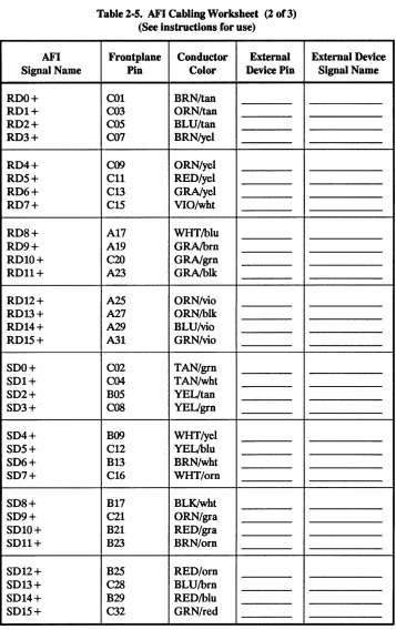
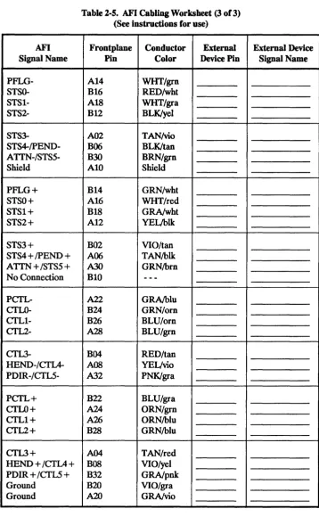
By following the wiring tables in this manual, you can fabricate a custom cable for your application. Be sure the total length is less than 3 meters to avoid noise and other transmission problems associated with single-ended applications. Use table 2-5, API Cabling Worksheet (later in this
chapter), to design the connections.
Figure 2-15 illustrates the way to make the cable. Cut off the connector and the grounding grommet from the unlabeled end of the cable. Using the information from table 2-5 that you will have filled in, wire the connec-tor that will attach to your external device.
Tables A-3 and A-4 identify each signal from the API or the external device (as well as ground return lines) used by the HP cables. If you design a cable, or the connector for the external device, use these tables to do so.
Table A-5 gives the cable pin assignments for both ends of the cables. Use the same twisted pairs and ground return lines as listed in table A-6 to gain the greatest possible noise immunity.
In the differential mode, both range and reliability are greatly improved over either single-ended mode. The supplied 3-meter or optional 12-meter cable will work in either high- or low-true mode, depending on the connector on the external device.
By following the wiring tables in this manual, you can fabricate a custom cable for your application. Use table 2-5, API Cabling Worksheet (later in this chapter), to design the connections. HP strongly recommends the length be less than 12 meters. Longer cables will reduce reliability by introducing detrimental signal characteristics, such as skew and attenua-tion.
Figure 2-15 shows how to make the cable. Cut off the connector and the grounding grommet from the unlabeled end of the cable so the conductor colors will match the table information. Using the information from table 2-5 that you will have filled in, wire the connector that will attach to your external device.
Wiring the
Custom AFI Cable
I
Note
I
Planning the AFI Cable
Making a custom cable for connecting the API to the external device requires that you plan the wiring and that you build the cable. This section explains these two steps.
When cutting the existing cable, be sure to keep the end labeled "Made in
V.SA." so the conductor colors will match the tables.
Table 2-5 is a worksheet you use to establish the pin assignments for the external device end of the cable. To use the table, frrst fill in the column labeled "External Device Signal Name" on the right side of the table for all three pages. Be sure to include the ground return lines for a single-ended application. See chapter 3 for a description of the mnemonics. These signals will be the complements of those listed in the left hand column. For instance: "RDO-" (frrst low received data line) on the API (in the left column) requires a connection either to a send (or transmitted) data line or to ground. Which one is correct depends on the logic sense and mode of your external device. Then write in the connector pin numbers corresponding to the signals you just filled in.
Figure 2-14 shows a portion of the table with the data filled in for signals in a single-ended, low-true application.
Fill in this column frrst. Fill in this column second.
/
""
AFI Frontplane Conductor "'.. External External 6evice
Signal Name Pin Color Device Pin Signal Name
RDO- A01 TAN!brn C04 TOQ
RD1- A03 TAN/orn C03
ill
1RD2- A05 TAN!blu C06
IJ22
RD3- A07 YEL!brn COS T03
Figure 2-14. Filling in the AFI Cabling Worksheet
Constructing the Cable
If you are constructing the cable in the previous example, solder the tan conductor of the tan!brown pair to pin C04 of the external device connec-tor. This will pass the frrst transmitted data signal (TDO) from the external device to the frrst low received data (ROO-) line on the API. Then con-tinue by soldering the tan conductor of the tan/orange pair to pin C03 on the connector, the tan of the tan!blue pair to pin C06, and so on.o
I
Note
I
This process does not take into account the layout of the connector youare working with. Use the most convenient order for actually attaching the conductors to your connector.
In table 2-5, the color in capital letters is the conductor used, the other color is its twisted-pair mate. Thus "TANlbrn" is the tan conductor of the tan!brown pair, and "YELlbrn" indicates the yellow wire of the
yellowlbrown pair.
, Labeled end of
AFIcable ~
(r-'--D-'--~D-"--Dr--r---'D-"--~ I=~
I
~
I API cable with
API device adapter
o
connector removed from non-Iabled end and
conductors attached to required connector pins
Figure 2-15. Wiring the Custom AFI Cable I
External device with existing connector
AFI Signal Name ROO- R01- R02- R03- R04- ROS- R06- R07- R08- R09- R010- R011- R012- R013- R014- R01S- SOO- SOl- S02- S03- S04- SOS- S06- S07- S08- S09- S010- SOll-SO 12-SO 13-SO 14-
SOlS-Table 2-5. AFI Cabling Worksheet (1 o(3) (See instructions for use)
Frontplane Conductor External
Pin Color Device Pin
A01 TAN/bm
A03 TAN/oro
AOS TAN/blu
A07 YELibro
A09 YEUoro
All YEUred
A13 YEUgra
A1S WHT/vio
C17 BLU/wht
C19 BRN/gra
B19 GRN/gra
C23 BLK/gra
C25 VIO/oro
C27 BLK/oro
C29 VIO/blu
C31 VIO/gro
B01 GRN/tan
B03 WHT/tan
C06 TAN/yel
B07 GRN/yel
C10 YEUwht
B11 BLU/yel
C14 WHT/bro
B1S ORN/wht
C18 WHT/blk
A21 GRAforo
C22 GRAfred
C24 ORN/bro
C26 ORN/red
B27 BRN/blu
C30 BLU/red
B31 REO/gro
External Device Signal Name
AFI Signal Name ROO + R01+ R02+ R03+ R04+ ROS+ R06+ R07+ R08+ R09+ ROI0+ ROll+ R012 + R013 + R014 + R01S+ SOO+ SOl+ S02+ S03+ S04+ SOS+ S06+ S07+ S08+ S09+ SOlO + SDll + S012+ S013 + S014 + SOlS +
Table 2-5. AFI Cabling Worksheet (2 of 3) (See instructions for use)
Frontplane Conductor External
Pin Color Device Pin
COl BRN/tan
C03 ORN/tan
COS BLU/tan
C07 BRN/yel
C09 ORN/yel
Cll REO/yel
C13 GRNyel
C1S VIO/wht
A17 WHT/blu
A19 GRAlbrn
C20 GRNgrn
A23 GRAlbIk
A25 ORN/vio
A27 ORN/blk
A29 BLU/vio
A31 GRN/vio
CO2 TAN/grn
C04 TAN/wht
BOS YEL/tan
COS YEL/grn
B09 WHT/yel
C12 YELlblu
B13 BRN/wht
C16 WHT/orn
B17 BLK/wht
C21 ORN/gra
B21 REO/gra
B23 BRN/orn
B25 REO/om
C28 BLU/brn
B29 REO/blu
C32 GRN/red
AFI Signal Name PFLG- STSO- STSl- STS2- STS3- STS4-/pEND- ATTN-/STS5-Shield PFLG+ STSO+ STSl+ STS2+ STS3+
STS4 + /PEND + ATTN + /STS5 + No Connection PCTL- CTLO- CTLl- CTL2- CTL3- REND-/CTIA- PDIR-/CTL5-PCTL+ CTLO+ CTLl+ CTL2+ CTL3+
REND + /CTIA
+
PDIR + /CTLS + Ground
[image:39.617.137.496.78.659.2]Ground
Table 2-5. AFI Cabling Worksheet (3 of 3) (See instructions for use)
Frontplane Conductor External
Pin Color Device Pin
Al4 WHT/grn
Bl6 RED/wht
Al8 WHT/gra
Bl2 BLK/yel
A02 TAN!vio
B06 BLK/tan
B30 BRN/grn
AlO Shield
Bl4 GRN/wht
Al6 WHT/red
Bl8 GRA/wht
Al2 YEL/blk
B02 VIO/tan
A06 TAN/blk
A30 GRN/brn
BlO
-
--A22 GRA/blu
B24 GRN/orn
B26 BLU/orn
A28 BLU/grn
B04 RED/tan
AOS YEUvio
A32 PNK/gra
B22 BLU/gra
A24 ORN/grn
A26 ORN/blu
B28 GRN/blu
A04 TAN/red
BOB VIO/yel
B32 GRA/pnk
B20 VIO/gra
A20 GRA/vio
External Device Signal Name
Installing the AFI
'100'U"O')
Selecting a Slot
I
Note
I
Orienting the
peA
Installing the device adapter into the host computer backplane is straight-forward:
• Select the appropriate host slot. • Orient the PCA correctly. • Insert it into the backplane. • Attach the cable.
Never install a peA with the power on. If you do, you risk serious electrical shock. The system manuals explain how to shut down the operating system and switch otT the host computer.
The default slot for the API is slot 5. To install the PCA in another slot, you must identify the slot to the operating system. This requires regenerating the kernel, a task more complex than this manual can address. To do so, see the HP-UX System Administrator's Manual for your computer. If you choose to install the API in a non-default slot, it must be in one of the frrst eight slots (0 through 7) of the CIO bus (CIB). If none of these is open, you will have to make one available by moving another device adapter. Check in the system manuals to determine which device adapters can go into the slots you have empty.
CIB slots are numbered in orange. Some computers offer the option of converting CIB slots into Mid Bus slots. In these computers, the slots may have dual numbering in other colors. Before installing the API device adapter, check the I/O configuration table in the system manuals.
If you have other PCAs in the host backplane, use the same orientation for the API. See figure 2-16. If the cables from these adapters exit toward the bottom of an adapter held vertically, and with the cable toward you, the component surface will be on the right.
Inserting the PCA
Connecting the Cable
Cable Connector
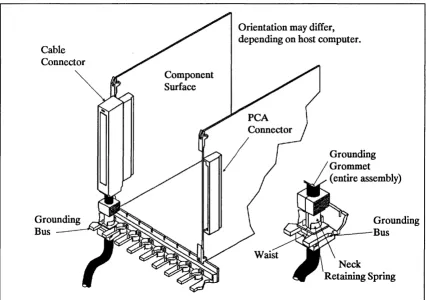
[image:41.613.124.550.305.605.2]Holding the PCA by its extractor levers, and with the component surface oriented correctly, insert the backplane edge of the PCA into the correct slot. After you have the API aligned in the slot guides, push it fully into the slot so that the backplane connector mates with the receptacle in the computer. This should not take a lot of pressure, and you will feel a dis-tinct snap as the connector seats. If it feels like you are pressing too hard, but not getting the desired result, remove the API and check for obstruc-tions, bent or broken pins, and so on. If there is damage, please call Hewlett-Packard for repairs.
Figure 2-16 shows the placement of the grounding grommet in the grounding bus of the computer backplane. See the detail section. The fmgers of the grounding bus should fit snugly on the short, square ''waist'' of the grommet. This is the grounding contact. Be sure it is secure. Some computers may not have a retaining spring, but if yours does, be sure it holds the grommet fIrmly on the long neck, as shown in the illustration.
Component Surface
Orientation may differ, depending on host computer.
Grounding Grommet (entire assembly)
Grounding
Bus ~-k~~~~,
Grounding Bus
Keltam~ Spring
Figure 2-16. A Typical AFI Installation
Startup and
Verification
Applying Power to the
peA
Configuring the
Operating
System
Testing the AFI
I
Note
I
The startup procedure involves:
• Applying power to the PCA.
• Configuring the API into the computer system (generating the kernel). • Testing the API using the diagnostic APIDAD.
To apply power to the API PCA, switch the computer on. Each system has its own procedure. Your system manual will have the details for this operation.
The HP-UX System Administrator's Manual (part number 5958-9513) explains how to regenerate the operating system kernel. This may take half an hour or longer.
Full testing procedures are in chapter 5, Hardware Troubleshooting. If
the PCA does not work, this test will identify the bad hardware portions. The required fix is to replace the API PCA.
Connecting the
Peripheral Device
Grounding the Cable
'Wf'hil'I')
There are three possibilities regarding the peripheral device for your application.
• Design the external device connector to meet the requirements of the API device adapter and the cable supplied.
• Use an existing device as is, and either:
• Use the male wire-wrap adapter to make an intermediate cable to connect it to the API device adapter.
• Customize the API cable for the external device.
• Rebuild the device connector for an existing device to the specifica-tions of the API device adapter cable.
Of the three, the fIrst is the most desirable. However, any of them is acceptable, and the information in this section will be equally valid for you. At this point, we remind you that the logic sense terminology used in this chapter refers only to the logic on the API device adapter hardware, and not to what you see from the host system. If you do not understand this concept, decide on a logic sense after reading the section titled "Logic Sense" later in this chapter.
You must ground the cable at the peripheral device for two reasons: • As a safety precaution: The grounding grommet exposes all potentials
to the environment. Grounding the cable reduces the danger of electrical shock.
• By grounding the cable, you reduce radiated noise from the shield. If
you fail to ground the cable, you may violate electromagnetic inter-ference, EMI, (also called radio frequency interinter-ference, RFI) regulations in your jurisdiction.
The total cable ground path (shield) resistance must not exceed 80 mQ. Higher resistance creates a shock hazard.
''In
did.)
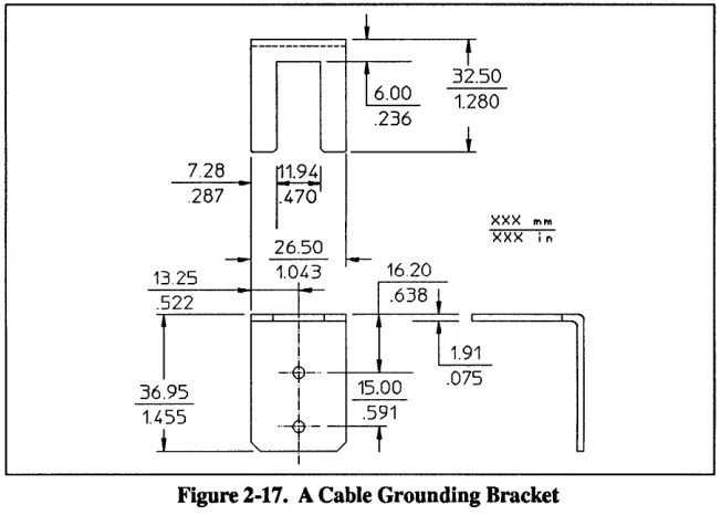
The supplied cable has a grounding grommet at both ends. A good way to ground the cable at the peripheral device is with a metal bracket to hold the grommet in the same manner as at the computer backplane. See figure 2-17. This bracket must have positive contact with the device chassis.
7.28 .287
,---
-+-.--~
.236
1.470
_ 26.50
-~
l
13.25 1.0,43 16.20
-.5-2-2---+----+--1- .638
t
t
32.50 1.280
XXX 11'1'"
I I
_·t-·
~
~
.07536.95
..
~
__~1
i r1.455
[image:44.612.222.548.160.393.2]i
Figure 2-17. A Cable Grounding Bracket
Be sure to isolate the grounding grommet from possible contact with people. Use a contact insulator ("shrink wrap" or insulating tape) or enclose it in a connector housing, similar to the cover on the host back-plane.
Attaching a grounding saddle (part number Al027-(0114), instead of the bracket above, to a connector housing (part number Al027-(0111) provides EMI shielding to reduce noise and interference with nearby devices. Installation of this housing depends on the design of your external device box; you would have to experiment to determine the best way to attach it. The housing must have positive electromagnetic contact around its periphery, ideally to a metal box surrounding the electronic components of your device.
Wiring the Peripheral
Device
I
Note
I
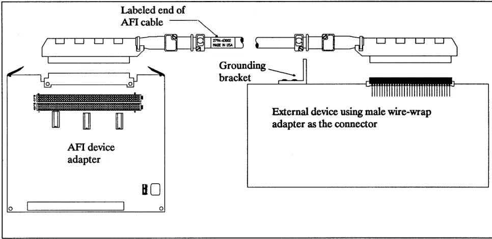
When designing the cable connector for the external device, you
can
use the male wire-wrap connector supplied, or any 96-pin DIN male connec-tor. Tables B-1 through B-6 give the information needed to design the connector or cable for your application. The connectors on the cable are DIN 41650 type "C" headers, also called "Eurocard connectors". If you need to create a custom cable, use table 2-5, the API Cabling Worksheet, to identify the cable connections and conductor assignments for the cable.When using the male wire-wrap connector included with the API, use the pin numbering scheme in figure 2-18. The molded numbers on the male connector do not match the numbers for the female cable connector.
A32
Existing female connectorA 1
1$~~~~~~~~~~~~~~~~~~:~:::~::::::*n_~IQ13II---'~
C32
C1
See numbering note in text. Male wire-wrap connector
A32
A1
Wire-wrap side
C1
Figure 2-18. The Wire-Wrap Pinout Orientation
I
Note
I
If you build a cable for a single-ended application, be sure to include theground return lines shown in table B-3 or B-4. These lines provide enough noise immunity to make a single-ended application work where it would not otherwise.
o
o
:; 51
Labeled end of
API cable --~
(r-~D"---'-D-'-D""""'--'-D-'----~i-T"""=---=NIJSA--'Ir--a~ ~'L---1~
0 0 0 0J
I I I~ __________ ~I
API device adapter
••
80
oGrounding bracket
[image:46.612.55.538.89.324.2]-External device using male wire-wrap adapter as the connector
Figure 2-19. The Wire-Wrap Adapter as the External Device Connector
Labeled end of _ _ ",-API cable
""-( 0 D O D
~I=-:::'I~ ~'L-
_ _~
I I
API device adapter
Bo
o
External device with existing connector
Wire-wrap adapter
as cable
[image:46.612.54.542.368.640.2]Logic Sense
Host
I
MidBus
SPU
Host
!
Mid BusSPU
Host
!
MidBus
SPU
Host
~
MidBus
SPU
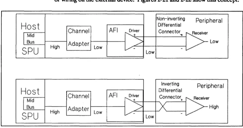
While the host computer and the Mid Bus pass a "I" from the program domain to the channel adapter as a high (
+
5 V) value, the channel adapter inverts all signals, in both directions. The API device adapter passes signals unchanged. If you wish to correct the inversion, there are two possibilities: Use the application software, or use "low-true" cabling or wiring on the external device. Figures 2-21 and 2-22 show this concept.Non-inverting Peripheral Differential
Channel AFI ~i:er Connector ..
[5=
>
LowAdapter
High Low /
-Low
Inverting Peripheral Differential
Channel AFI ~i:er Connector
: > r
+
>
HighAdapter
High Low
v-
[image:47.615.144.549.157.370.2]-Low
Figure 2-21. Differential Wiring for External Device Connector
For a differential device, build a connector to invert the signals as shown in figure 2-21. A single-ended device would use a connector as shown in figure 2-22.
High true
Peripheral
Single Ended
Channel
AFI
,,+
Driver Connector :;:eiverAdapter
/
~ Lowr - - -
-High Low
Low
Low true
Peripheral
l
Single EndedChannel
AFI
Driver .,l" Connector :;:eiver-~
S-LAdapter
-r~ High
High Low
v-
.p"'-High
Figure 2-22. Single-Ended Cabling to External Device
[image:47.615.142.548.428.635.2]3
Backplane
---a.--
---~---i
i
_L_
Theory
of Operation
The HP 27114B Asynchronous FIFO Interface (AFI) operates in half duplex mode. To the host and the peripheral it appears to be a FIFO buffer. The buffer stores up to sixty-four, 18-bit words (including two non-data status bits). There are three frontplane handshake modes: FIFO Mode, Master; Full Mode, Master; and Full Mode, Slave. A state machine controls the handshaking.
This chapter describes the signals, registers and major areas of the AFI device adapter. Since this manual covers only the hardware portion of the AFI product, we have included information about the software driver only when necessary to understand the hardware functions.
The three functional blocks are:
• Frontplane interface. • Midplane, which includes:
[image:49.612.70.555.410.694.2]• The handshake control state machine. • The FIFO buffer and other registers. • Backplane (channel) interface control circuitry.
Figure 3-1 shows the logical arrangement of the major components of the AFI in the planes.
Midplane
Frontplane
PDIR
i---T---i
--:-r~-:-~ Backplane Frontplane
---i
State MachineI
i
--1."_-=.-_
Data Bus
State Machine
FIFO
BufferFigure 3-1. The AFI Planes
Input Receivers Dir f---=R-ec-:ei-ve-=B::-"us---' Buffer I---~ Output I----=r:-ra-ns-m-:it---=-Bu-s----,
Dir
I
LatchI
Drivers
I
Note
I
The channel adapter (on the Mid Bus of the host computer) inverts all signals (data, control and status) going between the API and the host back-plane. Since the API device adapter does no corrective inversion, they remain inverted. (A "1" in the program domain becomes a low level on the API, a "0" becomes a high level.) To correct them, invert the signals in the program or implement low-true logic in the peripheral. Since the API uses differential drivers and receivers, each signal is available in both normal and inverted form. Unless noted, bit values in this chapter are from the program domain. Table 3-1 shows the conversion from the program domain to the API hardware domain.Table 3-1. Program Domain to AFI Hardware Domain Conversion
Application Program Domain
External Device Type 0 1
Differential, High-True
( + )
signal > (-) signal( + )
signal < (-) signalDifferential, Low-True
( + )
signal < (-) signal( + )
signal > (-) signalSingle-Ended, High-True signal
=
TTL high signal=
TTL lowFrontplane
Interface Control
Circuitry
Frontplane Signal
Definitions
RD[15:0]
SD[15:0]
The frontplane interface control circuitry consists of drivers, receivers and handshake control circuitry. The interface moves data between the API frontplane and the FIFO buffer, either as the master or slave of the hand-shake sequence between the API and the external device. Depending on the transfer direction, as data or space becomes available in the buffer, the frontplane control circuitry asserts a request to the peripheral to move data.
This section describes the API frontplane signals. The information given for each signal includes the name, a mnemonic, its function, the origin and destination, the hardware logic sense and, fmally, the frontplane pin this signal appears at in differential mode. This section references hardware logic sense as measured from the frontplane connector to the API logic. Signals going on to the host (RD[15:0], CfL[5:0], etc.) go through the CIB inversion process explained in chapter 2. Remember that in single-ended mode, the mode jumpers short either the (
+ )
or (-) signal to ground. The API uses MC 3487 drivers and 26LS32B receivers.Full Name: Read Data Bus. Origin: External device. Destination: API.
Hardware Logic Sense: High True.
Pin Assignment (Differential): Odd-numbered pins AOl through A19 and A23 through A31, pin B19, odd-numbered pins COl through C19 and C23 through C31, and pin C20. (See table A-2.)
Function: Read Data Bus receives the data from the external device. In word mode, the API uses bits RD[15:0], with RDO the least significant bit. In byte mode, the API uses bits RD[7:0], with RDO the least significant bit.
Full Name: Send Data Bus. Origin: API.
Destination: External device Hardware Logic Sense: High True.
Pin Assignment (Differential): Pin A21, odd-numbered pins BOl through B17 and B21 through B31, even-numbered pins C02 through CIS, pin C21, and even-numbered pins C22 through C32. (See table A-2.) Function: Send Data Bus sends data to the external device. In word mode, the API uses bits SD[15:0], with SDO the least significant bit. In byte mode, the API uses bits 8D[7:0], with SDO the least significant bit.
PCTL
PFLG
PDIR
CTL[5:0]
Full Name: Peripheral Control. Origin: API.
Destination: External device. Hardware Logic Sense: High True.
Pin Assignment (Differential): A22 and B22. (See table A-2.)
Function: When the API asserts PCfL, this signals the start of a data transfer. It means either that the outgoing data are valid or that new incoming data will be accepted.
Full Name: Peripheral Flag. Origin: External device. Destination: API.
Hardware Logic Sense: Low True (default, but the value of the edge bit can change this sense).
Pin Assignment (Differential): A14 and B14. (See table A-2.)
Function: When the external device asserts PFLG, this signals that the peripheral has accepted the data transferred or that there are valid incoming data from the device.
Full Name: Peripheral Data Direction. Origin: API.
Destination: External device. Hardware Logic Sense: N/A
Pin Assignment (Differential): A32 and B32. (See table A-2.)
Function: With PDIR high (+ >-), the API defmes the transfer direction as outgoing. A low (+ <-) PDIR signal means the transfer is incoming. You may deselect this signal in favor of CfLS in the application software. The default is PD IR.
Full Name: Control Bus. Origin: API.
Destination: External device. Hardware Logic Sense: High True.
Pin Assignment (Differential): B24, B26, A28, B04, AOB, A32, A24, A26, B28, A04, BOB and B32. (See table A-2.)
Function: When the API asserts one of the control signals, the peripheral
STS[5:0]
ATTN
REND
PEND
Full Name: Status Bus. Origin: External device. Destination: API.
Hardware Logic Sense: High True.
Pin Assignment (Differential): Bl6, Al8, Bl2, AD2, B06, B30, Al6, Bl8, Al2, B02, A06 and A30. (See table A-2.)
Function: When the external device asserts one of the status signals, the API responds according to the application program. Your program selects STS4 (the default) or PEND and STS5 or ATTN (the default).
Full Name: Attention. Origin: External device. Destination: API.
Hardware Logic Sense: Low True.
Pin Assignment (Differential): A30, B30. (See table A-2.)
Function: ATTN is an asynchronous interrupt line from the external device. When asserted, ATTN sets SENSE[ARQ]. The API will respond to the interrupt based on whether the application has enabled interrupts to the host. Your program may select either STS5 or ATTN (the default).
It may also disable ATTN.
Full Name: Host End. Origin: API.
Destination: External device. Hardware Logic Sense: Low True.
Pin Assignment (Differential): AOS, BOB. (See table A-2.)
Function: The API asserts HEND when the last output transfer is about to begin or when the last input transfer has just occurred. The application may select either HEND or CI'IA. The default is HEND.
Full Name: Peripheral End. Origin: External device. Destination: API.
Hardware Logic Sense: Low True.
Pin Assignment (Differential): A06, B06. (See table A-2.)
Function: The peripheral device asserts PEND to signal the end of the in-coming (to the API) transfer. Setup times for PEND must meet the same standards as for incoming data. By asserting PEND, the peripheral may also terminate an outgoing transfer. Your program may select either PEND or STS4. (The default is STS4.) It may also disable PEND.
Shield Ground
Signal Ground
Full Name: Shield Ground
Origin: N/A
Destination: N/A
Hardware Logic Sense: N/A.
Pin Assignment: AIO. (See table A-2.)
Function: Shield ground provides a safety and noise path to ground for any currents between differing ground potentials at the host computer and the external device. It requires a high-pass filter between the external device pin (AIO in the supplied cable) and the device safety ground. The filter may consist of a 50 V, .Ol,uF capacitor.
Full Names: Signal ground.
Origin: N/A
Destination: N/A.
Hardware Logic Sense: N/A.
Pin Assignment: A20 and B20. (See table A-2.)
Line Termination
Resistor Networks
Differential Line
Termination
Single-Ended Line
Termination
I
Note
I
In order to minimize power reflected to the receiver inputs, the API uses line termination for each input line.
Hewlett-Packard installs three line termination resistor network DIPs on each API. These networks (1810-0964) have their impedances matched to the impedance of the differential cables recommended with the device adapter. They provide a 120-0 connection between the (
+ )
and the (-) inputs for each line receiver. Each resistor dissipates 218 mW. If the maximum stable input differential voltage exceeds 4.6