Optical Designs for Improved Solar Cell
Performance
Thesis by
Emily Dell Kosten
In Partial Fulfillment of the Requirements for the Degree of
Doctor of Philosophy
California Institute of Technology Pasadena, California
2014
Acknowledgements
I am very grateful to the many people who helped make this thesis possible. Most importantly, I was very fortunate to have Harry Atwater as my adviser. He was endlessly supportive and enthusiastic, and his ideas and advice were crucial to much of this work. In addition, Harry taught me so much about crafting a paper and telling the story behind the science. Perhaps most importantly, though, the kind, collaborative research group he established was a wonderful place to work for five years.
The other students and post-docs in the Atwater group have been wonderful col-laborators and friends. While I am very grateful to all of the folks who helped create the friendly atmosphere in the group, there are many who require specific mention. First, Greg Kimball taught me how to be a grad student during my first few months in the group. I was also very fortunate to have Mike Deceglie, Adele Tamboli, Morgan Putnam, Dennis Callahan, Matt Sheldon, Victor Brar, and Dagny Fleischman as my officemates over the years. Mike, Adele, and Matt were very helpful as I was starting out, and all my officemates provided lots of useful and fun discussion.
Later on, the full spectrum team, consisting of Matt Escarra, Cris Flowers, John Lloyd, Sunita Darbe, Kelsey Whitesell, Michelle Dee, Carissa Eisler, and Emily War-mann, became close collaborators as well as a lovely group of friends. I am particularly grateful to John for his significant contributions to the light trapping filtered concen-trator work, especially the ray tracing. Cris also provided significant Python help which was crucial to automating the ray tracing work. Emily contributed substan-tially to the light trapping filtered concentrator work with cell bandgap optimizations, multijunction code, and detailed balance calculations. The advice and technical help she provided with the GaAs experiments, particularly contacting, were crucial. I have also very much enjoyed our chats over tea. In addition to our collaboration on the full spectrum project, Carissa provided significant expertise with photoluminescence measurements and sputtering, helpful discussion, and funny cat stories.
Wil-son all entered the group at the same time as I did. I have very much appreciated their friendship and help over the years. In particular, Hal provided significant useful dis-cussion on silicon solar cells, and Jeff and Sam were very helpful on device physics and fabrication questions. Carrie Hoffmann, Vivian Ferry, Imogen Pryce, Stan Burgos, Mike Kelzenberg, and Dan Turner-Evans provided significant mentorship and advice, with particular assistance from Dan and Mike on the silicon microwires project. Car-rie was also very helpful in her role as assistant director of the LMI-EFRC and adviser to the full spectrum project, and provided the LaTeX template files for this thesis. I’ve also appreciated technical help and discussions with Will Whitney, Ana Brown, and Nick Batara.
Jennifer Blankenship, Tiffany Kimoto, Lyra Haas, and April Neidholdt provided invaluable administrative support, as well as many enjoyable chats over the years. Their help with the administrative side was crucial to my graduate school experi-ence. Within the applied physics department, Christy Jenstad and Mabel Chik were also very kind and helpful with purchasing and administration. Donna Driscoll, the physics department coordinator, provided invaluable assistance as I navigated classes, qualifying exams, candidacy, and finally the thesis and defense.
samples.
Beyond my work friends, I’ve also greatly enjoyed the wonderful group of friends I’ve found in Pasadena. Emzo de los Santos, Branimir ´Ca´ci´c, Nate Glasser, Stephanie Barnes, Greg Loos, Betty Wong, Emily Capra, and Jackson Cahn were always up for boardgames, adventurous meals, and trivia, providing many a welcome break from work. I’ve also been lucky enough to have several old and dear friends, Carolyn Brennan, Katie Gose, and Leo Ungar, in Pasadena during graduate school, and it has been wonderful to spend time with them on a regular basis.
Finally, I’d like to thank my family. My parents introduced me to science and have always encouraged me. I’m very grateful for all their love, support, and interest in my work. I always look forward to seeing and hearing from my sisters, Sarah and Margaret. I really appreciate their love, and taking the time to visit and chat despite their own busy lives. Finally, I’d like to thank my husband, Joe Zipkin. He has been wonderfully helpful and loving through graduate school. I don’t know what I would have done without his care and support. I love you so, honey, and I’m so grateful for our little family of you, me, and the kitty.
Emily D. Kosten
May 2014
Abstract
Contents
List of Figures xii
List of Tables xv
1 Introduction 1
1.1 Motivation . . . 1
1.2 Solar Cell Fundamentals . . . 2
1.2.1 Solar Cell Structure . . . 2
1.2.2 Current: Absorption and Carrier Collection . . . 3
1.2.3 Current-Voltage Relationship . . . 6
1.3 Optics Background . . . 7
1.3.1 Ray Optics . . . 7
1.3.2 Lambertian Light Trapping Surfaces . . . 8
1.3.3 Interference-based Optical Coatings . . . 10
1.4 Overview of Thesis . . . 11
2 Light Trapping in Silicon Microwires 13 2.1 Motivation . . . 13
2.2 Modeling Wire Array Intensity Enhancement under Isotropic Illumi-nation . . . 14
2.2.1 Model Set-up: Balancing Fluxes . . . 14
2.3 Results for Wire Array Intensity Enhancement under Isotropic
Illumi-nation . . . 21
2.4 Modeling Wire Array Intensity Enhancement with a Lambertian Back Reflector . . . 23
2.4.1 Governing Equation: Back Reflector Model . . . 23
2.4.2 Evaluating Side Loss with Reflector Scattering . . . 25
2.4.3 Evaluating Side Absorption with Reflector Scattering . . . 27
2.5 Results for Wire Array Intensity Enhancement with a Lambertian Back Reflector . . . 29
2.6 Comparison of Model with Experimental Data . . . 31
2.6.1 Including Absorption in Ray Optics Model . . . 31
2.6.2 Experimental Methods . . . 32
2.6.3 Comparison of Model and Experiment: The Importance of Wave Optical Effects . . . 33
2.7 Conclusions . . . 35
3 Modeling the Effects of Angle Restriction 37 3.1 Angle Restriction and Photon Entropy . . . 37
3.2 Enhanced Light Trapping and Photon Recycling . . . 40
3.3 Detailed Balance Models . . . 41
3.3.1 Cells in the Radiative Limit . . . 41
3.3.2 Accounting for Non-Radiative Losses . . . 44
3.4 Absorptivity in Light Trapping and Planar Cells . . . 45
3.4.1 Accounting for Modal Structure . . . 45
3.4.2 Absorption in a Light Trapping Cell with Non-Ideal Back Re-flector . . . 46
3.4.3 Parasitic Absorption of Emitted Light in a Light Trapping Cell 48 3.4.4 Absorption in a Planar Cell . . . 49
4.2 Angle Restriction in a Light Trapping GaAs Cell: Limits to Efficiency 52
4.2.1 Cell in the Radiative Limit . . . 52
4.2.2 Effect of Auger Recombination . . . 53
4.3 Ideal and Non-Ideal Back Reflectors for a Light Trapping Cell . . . . 55
4.3.1 Effect of a Non-Ideal Back Reflector . . . 55
4.3.2 Dielectric Mirrors Approaching Unity Reflectivity . . . 56
4.4 Comparison with a Planar Cell Geometry . . . 58
4.5 Comparison to Previous Work: The Radiative Efficiency Approach . . 58
4.6 Radiative Efficiency in Current GaAs Cell Technology . . . 62
4.7 Broadband Angle Restrictor Designs . . . 63
4.8 Narrowband Angle Restrictor Design . . . 67
4.9 Conclusions . . . 75
5 Experimental Demonstration of Enhanced Photon Recycling in GaAs Solar Cells 77 5.1 Motivation . . . 77
5.2 Narrowband Multilayer Angle Restrictor . . . 79
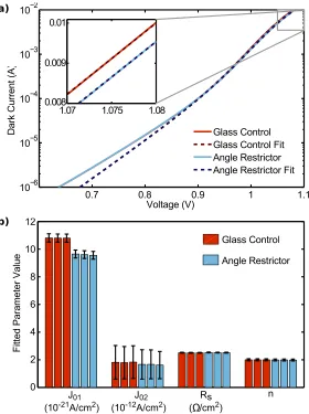
5.3 Dark Current Measurements . . . 82
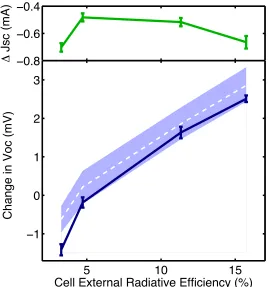
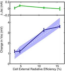
5.4 Voltage Enhancements Under Illumination . . . 84
5.5 Modified Detailed Balance Model . . . 86
5.6 Variable Angle Restrictor Coupling . . . 89
5.7 Bandgap Raising and Angle Restriction Effects . . . 92
5.8 Materials and Methods . . . 92
5.8.1 Cell Contacting and Characterization . . . 92
5.8.2 Optical Coupler Fabrication and Characterization . . . 93
5.8.3 Current-Voltage Measurements . . . 94
5.8.4 Implementation of the Modified Detailed Balance Model . . . 95
5.8.5 Gradual Coupling Measurements . . . 96
6 Angle Restriction in Silicon Solar Cells 98
6.1 Motivation . . . 98
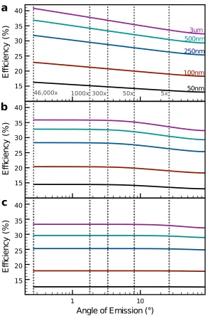
6.2 Effects of Angle Restriction in Ideal and Realistic Silicon Cells . . . . 101
6.2.1 Angle Restriction in Ideal Cells . . . 101
6.2.2 Angle Restriction in Realistic Cells . . . 103
6.2.3 Angle Restriction with External Concentration . . . 111
6.3 Angle Restrictor Designs . . . 114
6.3.1 Narrowband Angle Restrictor . . . 115
6.3.2 Broadband Angle Restrictor . . . 117
6.4 Conclusions . . . 120
7 Light-Trapping Filtered Concentrator For Spectral Splitting 122 7.1 Motivation . . . 122
7.2 The Light Trapping Filtered Concentrator . . . 126
7.3 Basic Design Considerations: The Multipass Model . . . 127
7.3.1 The Thick Slab Assumption . . . 127
7.3.2 Initial Subcell Optimization . . . 131
7.3.3 Reducing Probability of Slab Escape: Design Tradeoffs . . . . 131
7.4 Designing Omnidirectional Filters . . . 133
7.5 Optimizing Geometry and Filter Selection: Ray Trace Results . . . . 138
7.5.1 Filter Selection . . . 138
7.5.2 Subcell Re-Optimization . . . 140
7.5.3 Angle Restrictor Geometry Optimization . . . 143
7.6 Conclusions . . . 144
8 Conclusions and Outlook 146
List of Figures
1.1 Solar Cell Schematic: p-n Junction. . . 2
1.2 Solar Cell Bandgap and Current . . . 4
1.3 Light Trapping and Planar Geometry . . . 5
1.4 Current-Voltage Curve . . . 6
1.5 The 2n2 Light Trapping Limit . . . . 9
1.6 Reflectivity of Periodic and Aperiodic Thin Film Multilayers . . . 10
2.1 Schematic: Microwire Array without Back Reflector . . . 17
2.2 Light Trapping Factor Variation with Microwire Array Filling Fraction 22 2.3 Schematic: Microwire Array with Lambertian Back Reflector . . . 24
2.4 Variation of Power with Array Filing Fraction . . . 30
2.5 Comparison of Ray Optics Model to Experimental Absorption Mea-surement . . . 34
3.1 Photon Entropy Increase in a Conventional Solar Cell . . . 37
3.2 Photon Entropy in Concentrator and Angle Restrictor Systems . . . . 39
3.3 Light Trapping and Photon Recycling with Angle Restriction . . . 40
3.4 Balancing Photon Fluxes in the Detailed Balance Model . . . 42
4.1 Angle Restriction in a Light Trapping GaAs Cell . . . 54
4.2 Broadband Omnidirectional Dielectric Reflectors . . . 57
4.3 Angle Restriction in a Planar GaAs Cell. . . 59
4.4 Angle Restriction and Cell Geometry: Radiative Efficiency Model . . 61
4.6 Rugate Angle Restrictor Design . . . 69
4.7 Rugate Angle Restrictor Calculated Reflectivity . . . 71
4.8 Current Effects of Rugate Design . . . 72
4.9 Predicted Efficiency with Rugate Design . . . 73
4.10 Predicted Efficiency with Rugate Design and Concentration . . . 74
5.1 Enhanced Photon Recycling in a Planar GaAs Cell . . . 80
5.2 Narrowband Dielectric Angle Restrictor Design and Fabrication . . . 81
5.3 Dark Current Measurements and Fits . . . 83
5.4 Voltage Increase with Current Losses . . . 85
5.5 Voltage Increase with Equalized Currents . . . 87
5.6 Loss of Emitted Light From Sides for Variable Coupling . . . 90
5.7 Voltage Effects of Variable Angle Restrictor Coupling . . . 91
6.1 Angle Restriction in Silicon: Light Trapping . . . 99
6.2 Effect of Angle Restriction in Auger Limited Silicon . . . 104
6.3 Bulk Lifetime and Surface Recombination Estimation: IBC Cells . . . 107
6.4 Bulk Lifetime and Surface Recombination Estimation: HIT Cells . . . 108
6.5 Angle Restriction in HIT and IBC Cells . . . 110
6.6 Effect of Bulk Lifetime, Back Reflectivity, and Surface Recombination in Silicon Cells . . . 112
6.7 Effect of External Concentration with Angle Restriction . . . 114
6.8 Effect of Narrowband Angle Restrictor Design . . . 116
6.9 Effect of Broadband Angle Restrictor Design . . . 119
7.1 Efficiency Increases with Many Solar Cell Junctions . . . 124
7.2 Light-Trapping Filtered Concentrator . . . 126
7.3 Monte-Carlo Model to Determine Dielectric Slab Thickness . . . 128
7.4 Optical Efficiency with Multipass Model . . . 129
7.7 Parasitic Loss and Transmission Trade-offs . . . 135
7.8 Varying Cutoff Wavelength . . . 137
7.9 Reflectivity of Selected Filter Set . . . 139
7.10 Photon Flux at Each Subcell . . . 142
7.11 Angle Restrictor Optimization Sweep . . . 143
List of Tables
6.1 Cell Parameters for Ideal and Realistic Cell Models . . . 106
Portions of this thesis have been drawn from the following publications:
“Limiting Light Escape Angle in Silicon Photovoltaics: Ideal and Realistic Cells.” E. D. Kosten, B. K. Newman, J. V. Lloyd, A. Polman and H. A. Atwater, in prepa-ration.
“Experimental demonstration of enhanced photon recycling in angle-restricted GaAs solar cells.” E. D. Kosten, B. M. Kayes, and H. A. Atwater,Energy & Environmental Science 7, 1907-1912 (2014).
“Spectrum splitting photovoltaics: Light trapping filtered concentrator for ultrahigh photovoltaic efficiency.” E. D. Kosten, J. Lloyd, E. Warmann and H. A. Atwater,
Proceedings of the 39th IEEE Photovoltaic Specialists Conference (PVSC) 3053-2057 (2013).
“Highly efficient GaAs solar cells by limiting light emission angle.” E. D. Kosten, J. H. Atwater, J. Parsons, A. Polman, and H. A. Atwater,Light: Science & Applica-tions 2, e45 (2013).
Chapter 1
Introduction
1.1
Motivation
Solar energy is the world’s most abundant source of renewable energy. With an incom-ing power of 1.2x10⁵ terawatts, the solar resource dwarfs current worldwide energy consumption, estimated at 13 terawatts [1]. Despite the abundance of this renewable resource, fossil fuels provide greater than 80% our energy [1]. While previously the high cost of photovoltaics prevented more widespread adoption, recent developments in the Chinese solar cell industry have greatly increased production and reduced price. In fact, current module prices have allowed photovoltaics to achieve a levelized cost of energy similar to coal and natural gas, though the long-term sustainability of such prices is a matter of debate [2]. However, further cost reductions may yet be required for solar energy to become a substantial part of the energy portfolio, as these cost estimates do not include the storage necessitated by the intermittency of the solar resource.
increased cell cost, the cost per Watt will be reduced, as less cell area is required to produce the same amount of power. Furthermore, “balance of systems” costs, such as permitting, land, installation, and structural supports, are approximately half of the cost of a photovoltaic installation [3]. As many of these costs scale with area, improving cell efficiency also reduces balance of systems costs. With the exception of Chapter 2, this thesis will focus primarily on increasing efficiency for high performing cells as a means to reduce cost. The bulk of this thesis focuses on restricting the an-gles of emitted light to improve efficiency in gallium arsenide (GaAs) and silicon solar cells, two high performing materials. Finally, in the last chapter, we consider splitting light into separate spectral bands to improve the efficiency of high performing III-V solar cell materials.
1.2
Solar Cell Fundamentals
1.2.1
!"#$%&'()**"+#&)+,&-"./0"1+&!2+#%$&
Solar Cell Structure
•
!
31(&4"#$%&)501(*61+7&014)(&8244&9/0%&52&%$"8:2(&%$)+&%$2&)501(*61+&42+#%$;&
•
!
31(&8)(("2(&81442861+7&014)(&8244&9/0%&52&%$"++2(&%$)+&%$2&,"./0"1+&42+#%$;&
•
!
'$/07&,"./0"1+&42+#%$&9/0%&52&#(2)%2(&%$)+&)501(*61+&42+#%$;&
<)+,",)8=&>?)9& >9"4=&-;&@10%2+& A&
p-type n-type
[image:18.612.250.394.423.562.2]photon
Figure 1.1. Photons are absorbed by a solar cell to generate electrons and holes. These generated charge carriers are collected by a p-n junction, as shown above, or by some other form of selective contact.
While Figure 1.1 illustrates a planar p-n junction, not all cells utilize such a geometry. Furthermore, a p-n junction is not actually required, as all that is necessary are selective contacts to collect the electrons and holes separately. In silicon cells with an interdigitated back contact, for example, the bulk of the semiconductor has very low doping, and alternating n-type and p-type heavily doped regions at the back of the cell provide selective contacts to collect the electrons and holes respectively [4]. Finally, while many solar cells use homojunctions, where the selective contacts utilize the same material as the primary cell absorber, heterojunctions may also be utilized, where the selective contacts are formed from a different material than the primary absorber. Some III-V cells utilize this approach, as well as HIT (heterojunction with intrinsic thin-layer) silicon cells, where amorphous silicon is used to form the selective contact [5, 6].
1.2.2
Current: Absorption and Carrier Collection
The absorption in a solar cell is determined by the semiconductor bandgap. As shown in Figure 1.2, only photons with energy larger than the solar cell bandgap are absorbed by the solar cell, which limits the efficiency. In addition, high energy photons in this region are not utilized very efficiently, as the resulting carriers thermalize to the band edge, and are collected at the same voltage as lower energy photons. The short circuit current of a solar cell corresponds directly to the number of absorbed photons. Thus, the limiting short circuit current is determined by the number of photons in the solar spectrum that are above the band gap of the solar cell.
!"#$%&'(##&)$*+,*&
-& !+&.$/01$2&
p-type
n-type
!"
'"/03,4"/&&)$/0&5$#(/,(&& )$/0&
(6&
78&
•!
9.*"%.(0&27":"/*&1(/(%$:(&,$%%+(%*&
;7+,7&$%(&,"##(,:(0&.<&26/&=3/,4"/&
•!
'$%%+(%*&>%"?&27":"/*&;+:7&(/(%1<&
1%($:(%&:7$/&:7(&.$/01$2&:7(%?$#+@(&
[image:20.612.200.449.137.476.2]•!
A7":"/*&;+:7&(/(%1<&#(**&:7$/&:7(&
.$/0&1$2&$%(&/":&$.*"%.(0&
!"#$%&'()**"+#&)+,&-.((/+%&
-)+,",)01&23)4& 24"51&67&89:%/+& ;&
<:0&
=90& &
& &
-.((/+%&
=95%)#/& &
& & <:0&
>5)+)(&?95)(&-/55& !"#$%&'()**"+#&
?95)(&-/55&
[image:21.612.243.405.75.234.2]!"#$%&%()**"+#&#"@/:&"+0(/):/,&:$9(%&0"(0."%&0.((/+%&
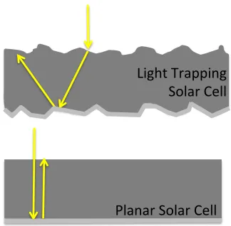
Figure 1.3. A light trapping geometry (top) enhances the light pathlength and resulting absorption relative to a planar geometry (bot-tom). Both cells have back reflectors.
Despite the thickness of current silicon cells, absorption is weak enough that light trapping is required to enhance the path length of light within the cell. Using a light trapping texture scatters the light, so it is trapped by total internal reflection, as shown in Figure 1.3. As will be further discussed in Section 1.3.2, this offers a significant path length enhancement relative to a planar cell. For direct bandgap materials, dual pass absorption, as shown in Figure 1.3, is sufficient, and cells generally utilize a planar geometry. A planar geometry also reduces surface recombination and easily accommodates epitaxially grown window layers, which are crucial for high quality III-V materials.
and the transfer of energy to the remaining carrier. This high energy carrier then thermalizes to the band edge, ultimately producing heat.
1.2.3
Current-Voltage Relationship
At short circuit, all photogenerated carriers are collected before excess carrier pop-ulation can build up within the cell. However, the excess carrier poppop-ulation within the cell leads to the cell voltage, and thus there is no voltage or power production at open circuit. At open circuit, in contrast, no carriers are collected, so the cell does not generate current or power. At open circuit, the excess carrier population and open circuit voltage (Voc) are determined by the balance between absorption and recombination within the cell. (This will be discussed more fully in Chapter 3.) As radiative recombination and absorption are set by the bandgap,Voc is generally 400-500 mV lower than the bandgap for high quality cells. A larger Voc-bandgap offset thus indicates that more non-radiative recombination is occurring in the cell.
!"#$%&'(&)&*"+)%&,$++&
,)(-'-)./&01)2& 02'+/&34&5"67$(& 8& 96.&
:".& !"#$%&!%"-;.'(<&=$<'"(&
&
,;%%$(7&
:"+7)<$&
>?$%)@(<&& !"'(7&
*"+)%&*?$.7%;2& A"74&B%$)C!6;(&
*'&D)(-<)?&
Figure 1.4. A schematic current-voltage curve illustrates short cir-cuit current, Isc, open circuit voltage,Voc, and the maximum power point where the cell operates. The area of the power producing region corresponds to the power produced at the operating point.
absorption and recombination in the cell, neither produce any power. The shape of the current-voltage relationship, or I-V curve, may be approximated as:
I(V)≈Isc−IoeqV /kT (1.1)
where I is the current, V the voltage, Io the dark or recombination current, q the electron charge, k the Boltzmann constant, and T the temperature. Because of the exponential shape, a small reduction in voltage relative toVoc, allows for currents near
Isc, as is shown schematically in Figure 1.4. Thus, a voltage somewhat less than open circuit allows for maximum power production in the cell. This voltage is known as the maximum power or operating point, and the voltage is referred to as the operating voltage (Vop) of the cell. The power generated by the cell at the operating point (Pop) is then:
Pop =I(Vop)Vop=F F IscVoc (1.2)
where F F is the fill factor of the cell, or the area of the rectangle representing the power producing region at the maximum power point divided by Isc,Voc product. The fill-factor indicates how “square” the I-V curve is and increased series resistance within the cell tends to degrade the fill-factor. The efficiency (η) of the cell is:
η= Pop
Psun
= F F IscVoc
Psun
(1.3)
where Psun is the power in the solar spectrum.
1.3
Optics Background
1.3.1
Ray Optics
For example, when modeling silicon solar cells, the largest wavelength of interest is about 1100 nm, and the the refractive index is about 3.5. Thus, the wavelength of light in the material is about 300 nm, and we can feel confident using ray optics assumptions for cells where the minimum dimension is at least 3 µm.
For cells that are thinner than the ray optic limit, optical guided modes develop within the thickness of the cell. These guided modes are based on the allowed solutions to Maxwell’s equations, and more guided modes are present for thicker cells. Once cells are in the ray optic limit, there are so many guided modes that they become a continuum of optical states corresponding to angles of light that lie outside the escape cone defined by total internal reflection. For cells thinner than the ray optic limit, we must account for the finite number of guided modes in considering light trapping within the cell. This will be discussed in more detail in Section 3.4.
For structures in the ray optic limit, ray tracing may be used to model the optical properties. These simulations consist of starting a certain number of rays, and using the Fresnel equations to follow their progress as they interact with various surfaces. Receivers are used to detect the final location of each ray and determine the per-formance. Both home-built and commercial ray trace software was utilized in this work.
1.3.2
Lambertian Light Trapping Surfaces
When considering light trapping, Lambertian textured surfaces are often considered as an ideal light trapping structure. These surfaces scatter light with equal brightness in all directions, similar to a white sheet of paper. Alternatively, the intensity is proportional to the cosine of the angle between the surface normal and the direction of observation. For solar cells, Lambertian scattering leads to significant light trapping benefits, including an approximately 50 times path length enhancment, for solar cells in the ray optic limit [7].
!"#$%&
%
$'()"*$!+,--(&)$'(.(*$
•
!
/,0,&1(&)$0()"*$(&$,&2$0()"*$34*5$&#)0#16&)$,783+-63&$
•
!
!#9*4+#2$:',.7#+6,&;$84+<,1#$81,=#+8$0()"*$
•
!
>&0?$@A%&
%$3<$+,&23.(B#2$0()"*$#81,-#8$
•
!
C&*#+&,0$0()"*$(&*#&8(*?$D$%&
%$E$(&1(2#&*$0()"*$(&*#&8(*?$
•
!
'()"*$*+,--(&)$<,1*3+$D$&
%$F(*"34*$7,1G$+#H#1*3+$
$
$
IJK$K-+(&)$I##6&)$%L@@$ M.(0?$NO$P38*#&$ Q$
M81,-#$ R3&#$
MO$S,703&3T(*1"$,&2$UO$R32?O$!"""#$%&'()#"*+,)#-+./,+(5$!"#$%&:%;$:@VW%;O$
R,&2(2,1?$M9,.$
Figure 1.5. For a solar cell with a Lambertian back reflector, in-coming light is scattered in all directions, but only light that is not totally internally reflected and lies within the escape cone can leave the cell. This leads to increased light intensity within the cell relative to the intensity of incoming light.
Under the principles of detailed balance, at steady state in a non-absorbing material, the light entering and escaping the material must balance. We assume an incoming light intensity Iinc, and a light intensity within the cell of Iint. However, the escape cone defined by total internal reflection allows only 1/2n2 of the light within the cell to escape, wherenis the cell index of refraction. Thus, for the outgoing and incoming fluxes to balance:
Iinc=
Iint
2n2 (1.4)
and
Iint = 2n2Iinc (1.5)
This is known as the ergodic light trapping limit. For a solar cell without a back reflector, the light intensity enhancement is n2 [7].
When weak absorption is included, the absorptivity of the cell, a, is:
a(E) = α(E)
α(E) + 4n12W
(1.6)
escape. We also see a 4n2, or approximately 50 times, path length enhancement, relative to a single pass through the cell. The additional factor of two relative to the probability of light escape is due to enhanced path length from light at oblique angles [7].
1.3.3
Interference-based Optical Coatings
In an optical thin film, interference occurs between light reflected at each interface, and the patterns of constructive and destructive interference result in the reflectiv-ity of the film. The simplest example is a single layer anti-reflective coating, where destructive interference of reflected beams leads to enhanced transmission. The prin-ciple is similar to impedance matching in electronics. With many alternating high and low index layers in an optical coating, known as a Bragg stack, high reflectiv-ity bands result from constructive interference of the reflections from each interface. While Bragg stacks are traditionally periodic, introducing aperiodicity into a Bragg stack can increase transmission around the reflecting band, as shown in Figure 1.6.
15
Emily Kosten [email protected] SPIE Optics and Photonics August 27th 2013
Aperiodic Dielectric Stack Filters
high index
low index
substrate
Aperiodicity allows additional design choices.
Stack filters may be omnidirectional with sufficient index
contrast and light incident from a low index material.
periodic aperiodic
To produce the interference effect, each layer in the thin film will have a thick-ness on the order of the wavelength of light. To model such structures, the transfer matrix method is traditionally used. In this method, the propagation of the electric field through each layer is represented by a matrix. The matrices for each layer are then multiplied together, and the resulting matrix is used to determine the electric field on either side of the optical multilayer, allowing the reflection and transmission coefficients to be determined. Essentially, this method provides a simple formalism for imposing the boundary conditions from Maxwell’s equations across each interface in the multilayer.
1.4
Overview of Thesis
Chapter 2
Light Trapping in Silicon Microwires
2.1
Motivation
Silicon nanowire and microwire arrays have attracted significant interest as an alter-native to traditional wafer-based technologies for solar cell applications [8-19]. Orig-inally, this interest stemmed from the device physics advantages of a radial junction, which allows for the decoupling of the absorption length from the carrier collection length. In a planar cell, both of these lengths correspond to the thickness of the cell, and high quality material is necessary so that the cell can absorb most of the light while successfully collecting the carriers. In contrast, a radial junction offers the possibility of using lower quality, lower cost materials without sacrificing performance [12, 13]. More recently, such arrays have been found to exhibit significant light trap-ping and absorption properties [8-10], and this absorption has been modeled in the nanowire regime with a variety of wave optical models [15, 20-24].
us to compare to the ergodic limit and consider wires of a different scale than those considered previously.
While much of the previous work has considered nanowires in the subwavelength regime, far below the ray optics limit, large diameter microwires can be grown by vapor-liquid-solid (VLS) techniques [8]. Previous device physics modeling suggests that for efficient carrier collection wires should have diameters similar to the minority carrier diffusion length, [13] and experimental measurements show diffusion lengths for VLS grown microwires of 10 microns [25]. Because wires with such diameters could approach the ray optics limit for solar wavelengths, it seems sensible to model these structures in the ray optics regime. In addition, comparison of the ray optics model with experimental data provides insight into the relative importance of wave optics effects for wires of various diameters.
We begin by assuming there is no absorption in the wires and examine the case for isotropic illumination so that we can compare to the ergodic light trapping limit for textured, weakly absorbing solar cells with a traditional planar geometry. To make this comparison, it is also necessary to postulate textured surfaces for the wires. We then examine the case of wires on a Lambertian back reflector, which are illuminated isotropically over the upper half sphere. Finally, we add a weak absorption term and find the absorption as a function of wavelength and angle of incidence, allowing us to compare with experimental data.
2.2
Modeling Wire Array Intensity Enhancement
under Isotropic Illumination
2.2.1
Model Set-up: Balancing Fluxes
we first imagine a hexagonal array of wires suspended in free space and isotropically illuminated. Furthermore, we assume that the wire surfaces are roughened such that they act as Lambertian scatterers. In other words, the brightness of the wire surfaces will be equal regardless of the angle of observation [26]. This fully randomizes the light inside the wires in the limit of low absorption, just as the roughened surfaces of planar solar cells do. The randomization of light within the wires serves to trap the light inside by total internal reflection.
With these assumptions in mind, we find the governing equation by simply bal-ancing the inflows and outflows of light within a single wire.
Iinc2AendT¯end+IincAsidesF¯=
Iint2AendT¯end
n2 +
IintAsidesL¯
n2 (2.1)
Above, Iinc is the intensity of the incident radiation, Iint is the the intensity of light within the wires, Asides is the area of the wires sides, Aend is the area of one wire end, and n is the index of refraction of the wire. In addition, ¯Tend is the average transmission factor through the end, ¯L is light from the sides which escapes the array, and ¯F is the incident light which enters through the sides.
The terms on the left hand side represent the energy entering the wire array, with the two terms representing the incident light which enters through the side and tops of the wire, respectively. For the top of the wire, the calculation is quite simple because there is no shadowing or multiple scattering, assuming that the wires are all the same height. Thus, we need only average transmission into the top over the incident angles to find ¯Tend. For light entering through the sides, we take into account transmission into the wire in addition to shadowing and multiple scattering. Thus, for a given incident angle, we determine ¯F, which gives the fraction of light transmitted through the sides, averaged over the angles of the incident radiation.
isotropic incident radiation, the averaged transmission fractor Tend is the same for incident and escaping light. For losses through the sides, much of the emitted light will be transmitted into other wires, and not lost from the array. Thus, an average loss factor, ¯L, is found, which gives the side losses that are not transmitted into other wires.
We rearrange the above equation to find the degree of light-trapping, or Iint/Iinc.
Iint
Iinc = n
2(2A
endT¯end+AsidesF¯) 2AendT¯end+AsidesL¯
(2.2)
Note that in the limit where the area of the sides goes to zero, the light trapping factor is n2, which reproduces the ergodic limit for a planar textured sheet that is isotropically illuminated, as we expect. If ¯F is larger than ¯L, the light trapping in this structure could exceed the ergodic limit. This seems unlikely, however, as time-reversal invariance would suggest that ¯L= ¯F because each path into the array must also be an equally efficient path out of the array. Furthermore, from a thermodynam-ics perspective, we expect that the light trapping in this structure should be exactly
n2. This is because the equipartition theorem states that all the states or modes should be equally occupied in thermodynamic equilibrium, and the density of states within the wires is n3 the of states in free space. (When calculating the intensity, it is necessary to multiply by the group velocity which goes as 1/n, such that the intensity is increased by n2 [7].) Thus, this case will allow us to assess the accuracy of the model and the assumptions necessary to simplify the calculation.
Averaging over all solid angles, with an appropriate intensity weighting, gives ¯Tend:
¯
Tend =
R2π
0
Rπ/2
0 T(φ) cos(φ) sin(φ) dφ dθ
R2π
0
Rπ/2
0 cos(φ) sin(φ) dφ dθ =
R2π
0
Rπ/2
0 Tncos
2(φ) sin(φ) dφ dθ
R2π
0
Rπ/2
0 cos(φ) sin(φ)dφ dθ
= 2 3Tn
2.2.2
Evaluation of Side Losses with a Radial Escape
Ap-proximation
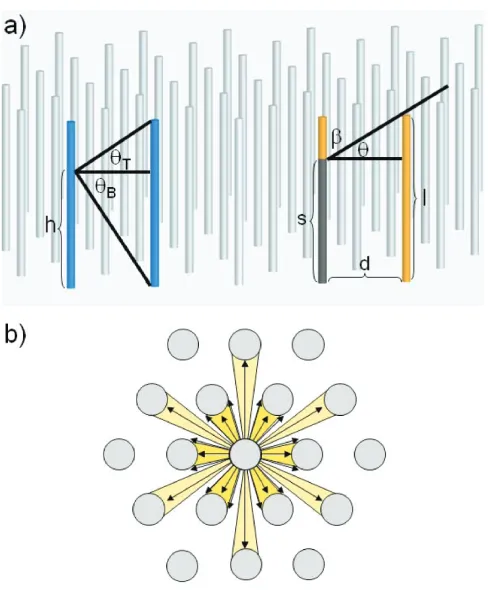
To calculate ¯L, we determine the fraction of light,g, escaping from the sides of a given wire that impinges on neighboring wires. Then we determine the transmission into those neighboring wires and the effect of multiple scattering from neighboring wires. To find g, we invoke a radial escape approximation where we treat each wire as if it were a line extending upward from the plane of the array. This approximation will be more accurate for low filling fraction arrays, because greater distance between the wires means that neighboring wires will more closely approximate line sources. The radial escape approximation serves to significantly simplify the treatment of the in-plane shadowing. With this assumption, we only need to calculate the portion of the in-plane angle that is subtended by wires at a given distance, and the losses associated with each distance in order to find g. As Figure 2.1b illustrates, the in-plane angle subtended by neighboring wires at a given distance is calculated geometrically.
The fraction of light that impinges on a wire a given distance away, f(h), is easily calculated from geometrical arguments and the properties of Lambertian surfaces, as Figure 2.1a illustrates. To simplify the calculation we ignore the increase in wire to wire distance as the wires curve away from each other. As before, this approximation will be more accurate for lower filling fractions, where the wires are farther apart and this effect will be smaller.
f(h) =
RθT
−θB cos(θ)dθ
Rπ/2
−π/2cos(θ)dθ
= sin(θT) + sin(θB)
2 (2.4)
To find g(d), we integrate f(h) over the height of the wire and normalize.
g(d) =
Rl
0sin(θT) + sin(θB)dh
2l =
√
l2+d2−d
l (2.5)
Tint(d), and take a weighted average to find the overall internal transmission factor,
Tint. Here, however, we must account for the curvature of the wire because this signif-icantly affects the angle the transmitted light makes with the wire surface. Assuming equal brightness for the allowed in-plane and out-of-plane angles, the expression for
Tint(d) is:
Tint(d) =
Rl
0
RθT −θB
Rα2
−α1Tncos
2(φ)dαdθdl
Rl
0
RθT −θB
Rα2
−α1cos(φ)dαdθdl
(2.6)
where the θ’s give the bounds of the out-of-plane angles, the α’s the bounds of the in-plane angles, and φ is the overall angle made with the wire.
To find ¯L we sum the losses in each pass through the wire array. For the first pass through the wire array, 1−g of light which left the wire side is lost, because it does not impinge on any of the other wires, and escapes. This is multiplied by ¯Tend because the light must leave the side of the wire before it can escape the array. On the second pass, the losses, L2, are as follows:
L2 = ¯Tendg(1−Tint)(1−g) (2.7)
This assumes that the reflected light has a uniform height distribution. In reality, more of the light emitted from the sides of the wires will impinge on the middle of the neighboring wire than either end, owing to the Lambertian distribution of light from the emitting wire. Thus, this assumption will overestimate the losses on succeeding passes through the array, but greatly reduces the computational intensity of the calculation by allowing for a generalization of the losses on theith pass through the array as:
Li = ¯Tend(g(1−Tint))i−1(1−g) (2.8)
This can easily be summed to give ¯L.
¯
L= ¯Tend(1−g)
∞
X
n=0
(g(1−Tint))n =
1−g
1−g(1−Tint)
2.2.3
Evaluating Side Absorption: Shadowing
In calculating ¯F, the main additional phenomenon we must address is shadowing. As Figure 2.1a illustrates, the shadowing fraction, u, as a function of wire to wire distance and angle of incidence is:
u(d, β) = l−s
l =
dcot(β)
l (2.10)
We then take a weighted average over the angle subtended at each distance to find
u(β), and also find the transmission factor for the incoming light as a function of β
by averaging over all in-plane angles α.
T0(β) =
Rπ/2
−π/2Tncos
2(φ)dα
Rπ/2
−π/2cos(φ)dα
(2.11)
As before, φ is the overall angle the incoming ray makes with the wire, which will depend on both α and β. Finally, we modify the multiple scattering model because light will only be reflected off the unshadowed portion of the wire, which will vary as a function ofβ. For the losses on the first pass through the array:
L1(β) =u(β)(1−T0(β))(1−g1(β)) (2.12)
Fori >1,
Li(β) = (1−g)u(β)(1−T0(β))g1(β)(1−T1(β))[g(1−Tint)]i−2 (2.13)
whereLi gives the losses on theith bounce, as before, andT1 andg1give the transmis-sion and impingement factors associated with the light reflected from the unshadowed portion of the wires. Summing to find the total losses:
Lt(β) =u(β)(1−T0(β))
1−g1(β) +
(1−g)g1(β)(1−T1(β)) 1−g(1−Tint)
Thus, for a given angle, β, the amount of light which is transmitted into the wires,
F(β), accounting for multiple scattering and shadowing is:
F(β) = u(β)−Lt(β) (2.15)
Averaging over all the angles of incidence gives ¯F.
¯
F =
R2π
0
Rπ/2
0 F(β) sin
2(β)dβdη
R2π
0
Rπ/2
0 sin
2(β)dβdη (2.16)
Above, η is the polar angle, sin(β)dβdη is the differential solid angle, and the addi-tional factor of sine gives the change in intensity with angle of incidence.
2.3
Results for Wire Array Intensity Enhancement
under Isotropic Illumination
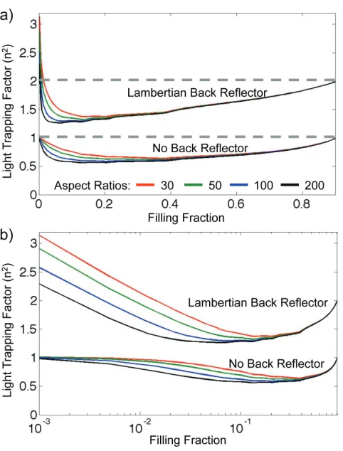
Inserting the expressions found above into Equation 2.2, we calculate the light trap-ping factor across a range of areal filling fractions, the fraction of the array covered by wires, for various wire aspect ratios. The results are given in Figure 2.2 and are indicated by the curves labeled “no back reflector”. For very large filling fractions we approach the ergodic limit, because the terms involving the wire sides become very small. We also reproduce the ergodic limit for very low filling fractions, where the radial escape approximation will be most accurate.1 In between the results fall below the ergodic limit, likely because the side loss factor, ¯L, is overestimated in the radial escape approximation. Because we expect thermodynamically that the result should be n2, this suggests that our approximations are reasonable, especially for low filling fractions, which are more likely to be of experimental interest. We also note that our
1Our model very slightly exceeds the ergodic limit across all aspect ratios for the smallest filling
fraction. This is observed across aspect ratios, with no trend with increasing aspect ratios. The
maximum amount by which the ergodic limit is exceeded is approximately 1% and is likely due to
results are closer to the ergodic limit for smaller aspect ratios. This is likely because the terms involving the wire sides are relatively smaller, and thus inaccuracies in those terms, such as overestimating ¯L, will have less impact. Thus, our approach reason-ably approximates the result we expect from thermodynamics, and the inaccuracies introduced by the radial escape approximation are well understood.
2.4
Modeling Wire Array Intensity Enhancement
with a Lambertian Back Reflector
2.4.1
Governing Equation: Back Reflector Model
We now investigate the effect of having a Lambertian back reflector with isotropic illumination in the upper half-sphere. In this case, no light will enter or escape through the bottom ends of the wires, which are covered by the back-reflector, and light that strikes the reflector will be scattered. In the planar case, the ergodic light trapping limit for such a geometry is 2n2, owing to the back reflector. Additionally, it seems that this geometry would give optimal scattering, as can be understood by basic physical arguments. Experimentally, it has been found that placing scatterers within the wire array can, in combination with a back-reflector, improve the performance of the array [8, 14]. This is because scatterers prevent light which is at normal or nearly normal incidence from going between the wires and bouncing off a planar back-reflector and out of the array. Imagine that we could place scatterers at any height level within the wire array. The light that scatters upward from the scatterers near the bottom of the array will be more likely to impinge on a wire, as Figure 2.3 shows. For optimal scattering, then, the scatterers should be placed at the bottom of the array. Since a Lambertian back reflector is similar to placing scatterers on a planar back reflector, this geometry allows us to investigate an optimal scattering regime as well as providing an interesting comparison to the planar case.
Figure 2.3. A schematic of the Lambertian back reflector case. The green wires show the effects of scatterers placed at different heights within the array. Note that for the lower scatterer light from a much smaller range of angles is able to escape. The purple wires illustrate the light which bounces off the reflector at a given point r
shown below.
IincAendT¯end+IincAsidesF¯0+IincAref lR¯0 =
IintAendT¯end 2n2 +
IintAsidesL¯0
2n2 (2.17)
The terms on the left give the light entering a wire, and the terms on the right give the amount of light escaping. Note that a factor of 1/2n2 replaces the 1/n2 factor because the back reflector doubles the intensity of the light within the wires [7]. In addition, ¯L and ¯F are replaced with ¯L0 and ¯F0, indicating that we need to account
for the Lambertian back reflector when calculating them. Finally, we note that there is a term accounting for the light that initially falls between the wires and strikes the reflector. ¯R0 gives the fraction of the light which initially strikes the back reflector
that subsequently enters a wire, accounting for shadowing and multiple scattering. With a one wire unit cell, Aref l, is simply the reflector area associated with a single wire. As before, we rearrange the above equation to find the relative intensities inside and outside the wire.
Iint
Iinc = 2n
2(A
endT¯end+AsidesF¯0+Aref lR¯0)
AendT¯end+AsidesL¯0
(2.18)
Once again, in the limit of zero side area, the light trapping reduces to the planar ergodic limit of 2n2, as expected.
2.4.2
Evaluating Side Loss with Reflector Scattering
To find the appropriate expressions for ¯L0we note thatgandT
intwill both be modified by the back reflector. Therefore, using the modified values of these, g0 and Tint0 , in our previous multiple scattering model gives ¯L0. To find g0, we tally the light lost.
Half of the losses from the non-reflector case remain, corresponding to the light that escapes from the top. The other half of the non-reflector losses are multiplied by the losses associated with light bouncing off the reflector and not striking a wire, Lref l.
As Figure 2.3 illustrates, we consider two wires a distance d apart, and of height
l, with the light being reflected from a point r on the reflector. The fraction of light which escapes at a given location on the reflector will be
L(r) =
RθT
−θBcos(θ)dθ
Rπ/2
−π/2cos(θ)dθ
= sin(tan
−1(r/l)) + sin(tan−1((d−r)/l))
2 =
r
√
r2+l2 +
d−r
√
(d−r)2+l2
2
(2.20) Summing the light coming from all points along the two neighboring wires and ac-counting for the Lambertian nature of the wire surfaces, we find the intensity of light at point r:
I(r) =
Z l
0
cos(η1)dh+
Z l
0
cos(η2)dh=
Z l
0
r
√
r2+h2dh+
Z l
0
d−r
p
(d−r)2+h2dh (2.21)
where η1 is the angle to the horizontal made by a ray escaping the wire at a height
h to strike the reflector at a point r, and η2 is the same quantity for the other wire. Averaging over all the points between the two wires with the appropriate intensity weighting gives:
Lref l(d) =
Rd
0 I(r)
r
√
r2+l2 +
d−r
√
(d−r)2+l2
dr
2Rd
0 I(r)dr
(2.22)
Lref l(d) is inserted into Equation 2.19 to findg0(d). We then take a weighted average of g0(d) with respect to the angle subtended at each distance to find g0.
To find Tint0 we note that light which impinges without striking the back reflector has a transmission factor which remains unchanged from the non-reflector case. Thus, once the transmission factor for light which bounces off the back reflector is calculated, these two transmission factors can be appropriately weighted together to give an overall transmission factor.
position along the reflector with a weighting to account for the varying intensity, as shown below.
Tref l(d) =
Rd
0 I(r)
Rπ/2
θT
Rπ/2
−π/2Tncos(θ) cos
2(φ)dαdθ+Rπ/2
θB
Rπ/2
−π/2Tncos(θ) cos
2(φ)dαdθdr
Rd
0 I(r)
Rπ/2
θT
Rπ/2
−π/2cos(φ) cos(θ)dαdθ+
Rπ/2
θB
Rπ/2
−π/2cos(φ) cos(θ)dαdθ
dr
(2.23) Sinceg0−g is the additional light impingement which results from light which has struck the back reflector, we find:
Tint0 (d) = g(d)Tint(d) + (g
0(d)−g(d))T
ref l(d)
g0 (2.24)
Then the overallTint0 is a weighted average with the in-plane angles subtended at each distance. Finally,g0 and Tint0 are used in place of their unprimed counterparts in the multiple scattering model (see Equation 2.9) to find ¯L0.
2.4.3
Evaluating Side Absorption with Reflector Scattering
To find ¯F0 we insert g0 and T0
int in the multiple scattering model in place of their unprimed counterparts. However, as Equation 2.14 shows, we also need to find T10
and g10. To find g01 we estimate the impact of the reflector, R, using the following expression:
R = (1−g1(d))−(1−g(d))/2 (2.25)
This estimates the amount of light that would be lost, but instead strikes the reflector. Because the top part will always be shadowed last, we assume the losses from the top are constant and equal (1−g(d))/2. Thus, everything else will strike the reflector, and we use our previous result for Lref l to find the total losses, 1−g01(d).
This allows us to modify the transmission factor:
T10(d) = T1(d)g1(d) +Tref l(d)(g
0
1(d)−g1(d))
g10(d) (2.27)
Inserting all the primed quantities for their unprimed counterparts in the equation for ¯F and dividing by two to account for the hemispherical illumination gives ¯F0.
Ob-viously, the shadowing fraction,u, and the transmission factor prior to any reflection,
T0, are unchanged by the presence of the reflector since the sun is directly striking the wire.
To find ¯R0, we first determine the shadowing of the reflector as a function of wire
to wire distance and angle of incidence. From Figure 2.3, the shadowed fraction of the reflector u(d, β) is:
u(d, β) = d−ltan(β)
d (2.28)
Taking a weighted average with respect to angle subtended at a given distance gives
u(β). We average over all β’s, including the differential solid angle and a weighting for intensity, to find u.
u=
Rπ/2
0 u(β) sin(β) cos(β)dβ
Rπ/2
0 sin(β) cos(β)dβ
(2.29)
Next we develop a multiple scattering model. The losses from light that doesn’t hit a wire after the initial reflection is Linc, which we find by averaging L(r) over the unshadowed portion of the reflector at each distance, with appropriate weighting for shadowing and the angle subtended at each distance. Tinc, the transmission of light after initial reflection, is found in an exactly analogous manner. (1−Linc)(1−Tinc) is reflected back into the array after bouncing once off the wire. From the previous result, (1−g0)/(1−g0(1−Tint0 )) of this light will be lost. Thus, the total losses for light that initially strikes the reflector are:
Ltot =Linc+ (1−Linc)(1−Tinc)
1−g0
1−g0(1−T0
int)
Then,
¯
R0 = (1−L
tot)u (2.31)
To find ¯R0, we have approximated the the shadowing of the reflector using the closest
distance between two wires, leading to an overestimation of the shadowing impact, which should be larger for high filling fractions. This is consistent with our use of the closest distance between two wires for wire to wire shadowing and losses.
2.5
Results for Wire Array Intensity Enhancement
with a Lambertian Back Reflector
Inserting the terms derived above into Equation 2.18, we find the light trapping factor, which is plotted as a function of filling fraction in Figure 2.2 by the curves labeled “Lambertian back reflector”. The results closely approach the relevant ergodic limit of 2n2 for large filling fractions as the terms involving the wire sides and the reflector become very small. As in the no back reflector case, the light trapping factor falls below the ergodic limit as the filling fraction is decreased from the maximum. It seems likely that, as before, the overestimation of ¯L in the radial escape approximation for these filling fractions is at least partially responsible for the decrease. This is supported by the trend in aspect ratios, which is similar to that for the no back reflector case.
Interestingly, we see that for small filling fractions, the light trapping increases asymptotically, significantly exceeding the ergodic limit, in contrast to the no back reflector case. As we previously noted, our approximations improve with decreasing filling fractions. Thus, there is no reason to suspect that surpassing the ergodic limit is an artifact of the modeling assumptions. Furthermore, we can understand the ob-served asymptotic increase physically by considering the limit of small filling fraction. For very small filling fractions, the side loss factor, ¯L0, and the side transmission
fac-tor, ¯F0, are nearly constant, as they have nearly reached their maxima. In addition,
exception of the back reflector term, are decreasing as the square of the radius. How-ever, the reflector area remains nearly constant with decreasing filling fraction, as the array is already almost entirely reflector. Thus, if ¯R0 is decreasing less quickly than
the radius squared, we should see asymptotic increase. In fact, fitting the asymptotic regions of each of the curves, we find that the curves are increasing as r−p, where p has values between 0.33 and 0.37. Figure 2.4 uses the fit in the calculation of the power to give a sense of the goodness of the fit. The fits are quite good across all the curves, and the values of p do not trend with aspect ratio. These fits suggests that the back reflector transmission goes approximately as the radius to the 5/3 power in the low filling fraction regime, across the range of aspect ratios explored here. The variation of the onset of asymptotic behavior with aspect ratio is also consistent with this explanation, as the denominator of the light trapping factor will decrease more rapidly for shorter wires.
volume of silicon, for an array with an aspect ratio of 50. We assume constant solar cell fill factor2 with increasing filling fraction, and assume that the short circuit current is proportional to the volume and the light trapping factor. For an axial junction, the open circuit voltage is proportional to ln(Jsc/J0), whereJsc is the short circuit current density andJ0 is the saturation current. We assume that for a light trapping factor of 2n2 the short circuit current density is 30 mA/cm2 and the saturation current density is 10−12 A/cm2. As Figure 2.4 illustrates, while the asymptotic increase does produce an increase in power per unit volume of silicon, as we expect, it does not produce an increase in the power per unit area. This is because the reduced volume of silicon per unit area leads to a reduced short circuit current, which is not overcome by the relatively small increase in open circuit voltage. Thus, in some sense, the Lambertian back reflector is acting as a concentrator, leading to increased power per unit volume of silicon at the cost of power per unit area.
2.6
Comparison of Model with Experimental Data
2.6.1
Including Absorption in Ray Optics Model
Absorption measurements have been reported as a function of angle of incidence and wavelenth for VLS-grown microwire arrays [8]. We therefore calculate the absorption for such an array in the ray optics limit. This will give us insight as to the importance of wave optic effects, and will allow us to determine the accuracy of the model for arrays at various scales. We consider an array embedded in PDMS, with a quartz slide underneath it. This very similar to the non-reflector case, except for the fact that we have PDMS/quartz (n=1.4) instead of free space. In addition, we include an absorption term in the governing equation. As Yablonovitch has shown, this term should be equal to 2αV Iint, whereαis the absorption coefficient, andV is the volume
2This should not be confused with the areal filling fraction of the wire array. As mentioned
previously, in solar cells the power can be calculated by multiplying the short circuit current, the
open circuit voltage, and the fill factor, where the fill factor accounts for the fact that the
where the absorption is occurring [7].
Thus, the governing equation for a given angle of incidence θ, is:
A0sidesImaxsin(θ)F(θ) + 2AendImaxcos(θ)T(θ) = 2αV Iint+
2AendT¯endIint
n2 +
AsidesLI¯ int
n2 (2.32) where Imax is the intensity of the incident light at normal incidence, and the factors of sin(θ) and cos(θ), account for the decreased intensity at non-normal incidence. Note that for the light entering through the sides we have A0sides instead a Asides, to denote that we need to account for decreased intensity as the wire turns away from the in-plane direction from which the light enters. Rearranging to find Iint gives:
Iint=
A0sidesImaxsin(θ)F(θ) + 2AendImaxcos(θ)T(θ) 2αV +2AendT¯end
n2 +
AsidesL¯
n2
(2.33)
The fraction of light absorbed, A, is:
A= 2αV Iint
AtotImaxcos(θ)
= 2αV(A
0
sidesF(θ) tan(θ) + 2AendT(θ))
Atot(2αV +2Aend ¯ Tend
n2 +
AsidesL¯
n2 )
(2.34)
whereAtot is the total area of one unit cell. With the exception ofA0sides, these terms follow directly from our previous work. However, between various in plane angles, the amount of shadowing will vary. Previously, to find ¯F we averaged this over all the in-plane angles. Experimentally, though, the light will only come from one in-plane direction, which in this case was aligned in the direction of maximal shadowing. In addition, to account for a non-free space medium, all the factors of 1/n2 are replaced with n2
1/n22, where n1 is the index of the embedding medium and n2 is the index of the wires, due to the relative density of modes between the two media.
2.6.2
Experimental Methods
catalyst islands. Wires with a radius of 1µm were grown from a hexagonally packed mask with 3µm diameter holes with a center to center spacing of 9µm. Larger wires with a radius of approximately 4 µm were grown from a hexagonally packed mask with 15µm diameter holes and 30 µm center to center spacing.
After growth, the metal VLS catalyst was removed from the wires and the height and diameter of the wires were measured using scanning electron microscopy. The wires were embedded in polydimethylsiloxane (PDMS, Sylgard) as reported previ-ously [27]. The PDMS was dropcast onto the wires and spun at 3000 rpm, and then cured at 120 ◦C for 30 minutes. Wires were removed from the substrate by scraping the PDMS film with a razor blade. Integrated reflection and transmission measure-ments were performed with a custom-built 4 inch integrating sphere apparatus using a Fianium supercontinuum laser illumination source and a 0.25 m monochromator [8]. The absorption of each sample was determined from the wavelength and angle resolved transmission and reflection measurements [13].
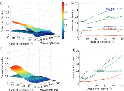
We then input structural parameters, as determined by SEM, from these measured arrays into the model developed above. The PDMS embedding material was included in the model, but the PDMS/air interface was neglected. (The PDMS/air interface gives about 3% reflection.) For each angle of incidence and wavelength we found the various absorption and loss terms, using wavelength specific n and α data. For wires with an approximately 1µm radius, results are given in Figure 2.5a and b. We also compare to wires with a radius of approximately 4µm and a similar aspect ratio, which should be closer to the ray optics limit. The results are shown in 2.5c and d.
2.6.3
Comparison of Model and Experiment: The
Impor-tance of Wave Optical Effects
Figure 2.5. a)The outlined surface gives the model output for wires with a 4.9% filling fraction, a 1 µm radius, and a height of 44 µm. The upper surface is the experimental result for such an array. b) The solid lines show the experimental data for various wavelengths, and the dotted lines show the model output. Note that even for the low absorbing 1000 nm curves, the model significantly underpredicts the absorption. c) The outlined surface gives the model output for wires with a 7.3% filling fraction, a 4µm radius, and a height of 160
incidence, we see that the model produces values similar to the filling fractions, and the 4µm array gives a value fairly close to the filling fraction, with 11% absorption for a 7% filling fraction. However, for the 1µm array we see 23% absorption for a 5% filling fraction, suggesting a significant wave optic effect in this regime. In fact, it is well known that particles on the order of the wavelength of light can have scattering and absorption cross sections considerably larger than their physical size, whereas in ray optics the cross section corresponds to the physical size [28]. It seems likely that this effect is causing the enhanced absorption observed in the smaller wires.
Despite the reasonable agreement for angles of incidence relatively near normal, the ray optics model fails to capture the strong increase in absorption observed with large angles of incidence for wavelengths where the absorption is strong. However, our model assumes that the light is fully randomized before any significant absorption takes place, which will not occur in strongly absorbing wavelength regimes. Thus, it is not surprising that our model fails to explain this behavior. As we expect, the agreement is improved for wavelengths where the absorption is low and this randomization condition is more accurate, as is shown in Figure 2.5d. However, even in this case, the shape of the curve is not captured particularly accurately, most likely due to differences between the experimental and modeled wires. For example, if the experimental wire surfaces were not perfectly Lambertian, but somewhat specular, the angular profile would likely be sloped across a wider range of angles, as is seen here. This is because the light which strikes the wire sides would reflect in one direction rather than be scattered in all directions, so light at near normal incidence would be less likely to enter the sides than for specular wires. Thus, our model works reasonably well in the low absorbing ray optics regime, but does not quite capture the angular dependence, perhaps due to non-Lambertian experimental wire surfaces.
2.7
Conclusions
case, the model produces light trapping close to the ergodic limit of n2 for filling fractions approaching zero and approaching unity. This conforms with our thermo-dynamic expectation and allows us to understand the accuracy of the approximations used for computational feasibility. In addition, it confirms our physical expectations about the regimes for which the approximations will be most accurate.
Applying the model to the case of a Lambertian back reflector, we observe signifi-cant intensity enhancements, including asymptotic increases for small filling fractions that significantly exceed the ergodic limit of 2n2. Quantitatively, for a filling frac-tion of 0.1%, the enhancement can exceed 3n2, and the asymptotic increase goes approximately asr−1/3, where ris the wire radius. These asymptotic increases result from the reflector acting as a concentrator. Fitting these results gives insight into the asymptotic behavior of the transmission factor for light that initially strikes the reflector, which goes as approximately r5/3. It seems that a more sophisticated back reflector, which preferentially scattered light sideways, could allow for asymptotic behavior which would be even more dramatic, a topic that deserves further study. However, while the asymptotic increases found here do give increased power per vol-ume of silicon, there is reduced power per unit wire array area, owing to reduced silicon volume at low filling fractions.
Chapter 3
Modeling the Effects of Angle Restriction
3.1
Angle Restriction and Photon Entropy
Under direct sunlight, conventional solar cells emit light isotropically, while receiving light only from the angles spanned by the solar disk, as shown in Figure 3.1. This increase in the angular distribution of light corresponds to an increase in the photon entropy, and the inherent entropy increase reduces the solar cell efficiency [29-32]. Thus, efficiency may be increased by reducing the angular spread of emitted light
!"#$%&'(&)*+,-.&
&
/01'&2*34*356*.&7-"#.53&&
8-93:53%&;<=&;>?@&
&
&
A#"#6.B&!"#++#*.&0.B$-&C*3&D"43*E-F&
7*$53&2-$$&G-3C*3"5.H-&
from the solar power conversion system.
Figure 3.2 illustrates two possible approaches to reducing the photon entropy in-crease. Most commonly, concentrating solar systems partially exploit this angular photon entropy term by redirecting the solar cell light emission into a narrow an-gular range, as shown in Figure 3.2a. As is well known from deployed systems and experimental measurements of solar cells under concentration, this leads to efficiency increases at low to moderate concentration ratios, due to increases in the solar cell voltage. While higher concentration ratios further reduce the angular spread of emit-ted light and resulting photon entropy increase, they do not practically realize the further efficiency gains that would be expected. At high concentration and the re-sulting high current densities, increased series resistance and heating degrade the cell efficiency, so that maximum efficiencies are achieved around a few hundred suns for typical high concentration cells, rather than the approximately 46,000 suns possible at maximum solar concentration [33-35].
!"
#"
3.2
Enhanced Light Trapping and Photon
Recy-cling
Benefits of Angle Restriction
!"#$%&'()**#%+,#-"."#/0))+"#!"""#$%&'()#*'#"+,-)#.,/)#1234456473648#9:8;<="# #
#
Scattered incoming light is less
likely to escape, leading to
longer path length and more
absorption in a thinner cell
#
#
#
Light Trapping
Photon Recycling
Light emitted via radiative
recombination is less likely to
escape and more likely to be
re-absorbed
."#-%0>#)?"#%*"#0)#122+)#345()#;69;=#7@<A37@AB#9:88A="# #
#
Escape angles without coupler
Solar Cell
Angle Restriction Optic
Textured Back Reflector
Emitted Light Incoming Light1&C*D#2"#EFG?)+#H#.?I%?)0#/0FJ'#
Figure 3.3. With angle restriction, the escape cone within the cell is narrowed. The dotted lines illustrate the escape cone and corre-sponding range of emitted angles without angle restriction, and the solid lines indicate the escape cone and emitted angles under angle restriction. The narrowed escape cone leads to enhanced light trap-ping of incoming light (left), as well as enhanced photon recycling of emitted light (right).
(Equation 1.6) for the absorptivity in a light trapping cell:
a(E) = α(E)
α(E) + sin4n22(Wθ)
(3.1)
where θ is the emission angle of the solar cell [7, 30, 36]. Note that this expres-sion reproduces Equation 1.6 where there is no angle restriction (θ = 90◦). Most importantly, angle restriction allows for full light absorption in a thinner cell.
Enhanced photon recycling occurs because radiatively emitted photons that would otherwise leave the cell are reflected back by the narr