High Frequency Behavior of High Power IGBT Modules
Carmine Abbate
1,*, Roberto Di Folco
21DIEI, University of Cassino and Southern Lazio, Via G. di Biasio, 43, 03043 Cassino (FR), Italy 2A.P.F.F Cassino Via San Marco, 03043Cassino (FR), Italy
*Corresponding Author: c.abbate@unicas.it
Copyright © 2015 Horizon Research Publishing All rights reserved.
Abstract
Sharp voltage gradients act as a stimulus for high power IGBT modules, which can exhibit a potentially instable high frequency behaviour. In effect, they can act as a radio frequency (RF) amplifier and under certain operating conditions the interaction between the device and the control or the external circuit can cause self-sustaining oscillations or the enhancement of the unevenness in current distribution inside a power module and that can have a significant impact on the reliability of the power converter. Moreover, this RF amplification worsen the generated EMI (Electro Magnetic Interference). This paper presents an extensive experimental investigation about the high frequency behaviour of IGBT high power modules. Measurements were performed by an original experimental set-up that was specifically conceived and constructed. Data were analysed with the help of a theoretical small signal model which was able to describe RF behaviour of high power IGBT modules.Keywords
IGBT Modules, IGBT Instability, High Frequency Behavior1. Introduction
The IGBT has become the mainly used power semiconductor device in modern power converter circuits in medium and high voltage applications. Even if these modules are designed to operate at relatively low frequency, typically < 5kHz, they can produce high frequency oscillations which turn out from the interaction between the device, the driver and the converter circuit. These oscillations are recognized to be the main cause of EMI (Electro Magnetic Interferences) emission and, in some circumstances, they have been recognized to cause a significant reduction of the converter reliability [1]. The high frequencies oscillations can be mainly attributed to the IGBT internal capacitances and inductances stray elements [2] that, suitably stimulated, can resonate both internally to the module and with the external circuit [3, 4]. In particular it was found that the main stimulus to the electromagnetic noise emission is attributed to the voltage gradients [3].
In addition to these problems, it was found [5] that IGBT
devices can exhibit a significant voltage amplification at high frequency so that the problems of the oscillations can be further enhanced. Due to this amplification, the RF oscillations can become self-sustaining thus further reducing the reliability of the converter. Methods for minimizing RF oscillations of IGBT were presented in literature based on a careful design of PCB layout and gate driver [6]. Moreover, the IGBT amplification phenomena can become relevant if the driver circuit generates high frequency conducted noise components, that can be transferred to the power stage and amplified, generating very high EMI levels.
In order to predict and reduce the EMI in power converter, it is very important to analyse the noise oscillations under different electrical IGBT module conditions that can be experienced during the normal device operations. For this reasons, a model for high frequency behaviour of IGBT modules was presented [3], which however is not able to include their amplification effect. This effect was found to play a major role in causing electrical instabilities of the current sharing among the chips of the module [2]. In this latter paper a small signal circuit model of IGBT devices was presented for single chip IGBTs. Additional data on analysis of single chips IGBT devices are also reported in [5].
The objective of this paper is to present an experimental study about the high frequency amplification observed in high voltage, high current IGBT module as a function of the driving and power parameters. An original experimental set-up was constructed for studying the small signal behaviour of these modules in a single device commutation in order to reduce the power dissipation on the device. The experimental characterisation is intended to point out a complete high frequency small signal model of high power IGBT modules that includes the RF voltage amplification effects.
2. Experimental Set Up
power dissipation that would demand a cumbersome and expensive cooling system. This problem has been surpassed by pointing out an original single shot measurement method described in the following.
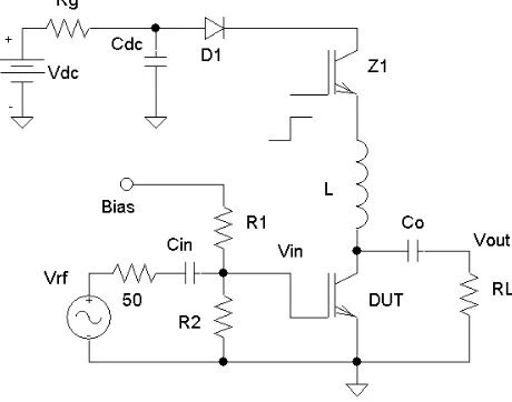
The simplified electric schematic of the experimental set-up is reported in Figure 1. A last generation 1200A-3300V IGBT module has been adopted as device under test (DUT) and connected to common emitter topology. The main components of the proposed circuit are: RL=50Ω, L=100µH, Cdc=2800µF. The inductor L dynamically isolates the biasing circuit from the device. The Z1 high voltage and current switch allows us to apply the voltage and current to the DUT in single shot operation. The required energy during the test is stored in the capacitor Cdc=2800µF by means of a variable power supply Vdc. When Z1 is turned-on, the voltage is quasi-statically applied on the collector of the DUT whereas the collector current reaches the value defined by the IGBT output characteristic that is fixed by the gate voltage (see the waveforms of Figure 2A that shows the typical voltage and current waveforms across the device under test during the operation of the circuit). The figure refers to a test with Vdc=300V, gate voltage VGE=6.8V, collector current Ic=100A. We can remember that for this class of the device, the gate voltage threshold is about 5.5V. This means that in our experiment the device is forced in its active region. In order to avoid extra voltage across the devices due to the inductance, the Z1 switch is turned off only after the voltage across Cdc capacitor becomes zero in order to have a zero current into the inductance.
Figure 1. Electric Schematic of experimental test set-up
A high frequency small signal voltage is injected to the gate of the IGBT during the whole voltage evolution by means of a commercial high frequency generator. As a consequence, the input voltage produces an high frequency output signal across RL. The diode D1 avoids that the current flowing into the circuit becomes negative during the low frequency resonating oscillation between Cdc and L. Moreover, in order to maintain the gate voltage at a constant
level during the circuit operation, the resistor R1 (see the Figure 1) must be carefully chosen. In particular, the value of this resistance could be very low in order to avoid that the IGBT stray Miller capacitance Cgc injects a very high additional current into the gate during the commutation, causing the IGBT to turn-on. Nevertheless its value could be chosen high compared with the source generator output resistance, in this case 50Ω, in order to avoid additional input attenuation. As a compromise, in our experiments the value of R1 has been set to 1kΩ.
3. Experimental Results
3.1. Typical Radio Frequency Behaviour
The high frequency IGBT module behaviour has been investigated by several experimental tests whose results are presented in this paragraph.
As indicated in the previous section, Figure 2A shows the typical voltage and current waveforms across the device under test during the operation of the proposed test circuit. In this case the gate voltage has been set to 6.8V and the collector supply voltage to 300V. The gate static polarization determines a collector current of about 100A, as given by IGBT output characteristics reported in the datasheet. The Vrf input high frequency voltage has been set in order to have 25mV peak to peak amplitude on IGBT gate. The corresponding frequency has been set to 1MHz. The resulting output radio frequency signal can be recognised as an overlap on the IGBT current and voltage waveforms (see Figure. 2A). The output voltage, Vout, is reported in Figure. 2B from which we can see that a relevant amplification (about 40dB) that can be attributed to the IGBT module. In fact the peak to peak output voltage is about 2.5V in these test conditions. The inset, that reports a zoom of the Vout waveform, allows us to recognize a 1 MHz sinusoidal tone.
This preliminary analysis confirms the IGBT module high frequency amplification phenomena during its quasi-static operation into active region.
[image:2.595.62.292.454.635.2] [image:2.595.313.553.579.735.2](B)
Figure 2. Collector current and voltage waveforms (A) and output voltage with the respective zoom (B)
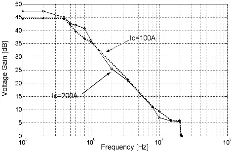
3.2. IGBT High Frequency Bode Amplitude Response
In order to understand the high frequency IGBT operation, it is very important to investigate on the RF frequency gain variation for different load currents and voltage values. For that aim, a sinusoidal variable frequency tone has been injected on the IGBT gate, measuring the corresponding output voltage. As experimental result, we have obtained the amplitude frequency response reported in Figure 3, measured in the range 100kHz – 40MHz for a supply voltage of 350V. In detail, the solid line is obtained for the collector current equal to 200A and the dotted line is related to amplitude Bode diagram for a collector current of 100A. The phase response has not been measured because in this paper the system stability has not been examined.
Figure 3. Voltage gain as a function of the frequency of the input signal for two collector current values
The curve are very interesting and confirms the IGBT module low pass behaviour. We can individuate the 3dB cut-off frequency at about 400kHz and the transition frequency (the gain become 0dB) at about 22MHz. In the stop band, the attenuation slope is about 30dB/dec. As far as the behaviour in the centre band, we can recognize that the voltage gain increases if the collector current is increased. In
particular, in Figure 3 we can see that the voltage gain increases with the collector current, according with the theoretical consideration that the device trans-conductance is related to the static collector current. Instead in the stop band the behaviour is practically independent from the collector current value.
3.3. Gain Dependence of the Current and Voltage Level
In the previous section we have recognized that the voltage gain is directly related to the collector current. This is confirmed by Figure 4 that reports the small signal voltage gain measured at centre band as a function of the collector current. The relationship between these two quantities, obtained by experimental approach, confirms that the voltage gain increases when the collector current is increased. Some analytic considerations about this relationship will be reported in the next sections.
Figure 4. Voltage gain as a function of collector current @ Vdc=350V and f=200kHz
Regarding the gain dependence of the voltage value, we have observed that into the IGBT centre band, the voltage gain, is practically independent of the collector voltage. Instead, the gain into the attenuation band, that is the range of the IGBT frequency response between the 3dB cut-off and transition frequency, depends on the collector voltage.
[image:3.595.314.548.305.454.2] [image:3.595.59.293.480.633.2] [image:3.595.315.549.573.725.2]Figure 5 reports the IGBT measured voltage gain as a function of dc voltage level for three different input frequency signals at Ic=200A. The upper curve refers to the gain variation for an input frequency of 100kHz, the middle curve to the gain variation at 1MHz and the lower one for 3.5MHz. The figure shows that in the attenuation band, the voltage gain increases with the dc voltage level.
4. High Frequency IGBT Module Model
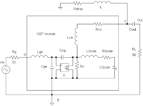
The high frequency IGBT module behaviour found by experimental measurements can be explained by an appropriate device model that accounts for the high frequency parasitic elements. The IGBT module model proposed here is an evolution of the model proposed in [3]. In particular the previous model describes the main device stray capacitances and inductances, but it does not consider the IGBT active amplification. Regarding the model topology, we can remember that the IGBT modules are composed of several elementary chips, generally obtained by the same silicon wafer, then with very similar physical characteristics, which are parallel connected. All internal connections constitute stray inductances which may resonate with internal equivalent capacitances, that generates, during the commutations, some oscillating noise components. Moreover, the IGBT module includes in the same case the reverse recovery diode which is still parallel connected and acts as a parasitic variable voltage capacitance [3].
Figure 6. Simple IGBT module model accounting the high frequency behaviour
Starting from these considerations, we can propose the IGBT radio frequency model of Figure 6 that describes its frequency behaviour by means of lumped elements. The circuit reported in Figure 6 outside the box, represents the external equivalent circuit used to polarize the IGBT module. The IGBT radio frequency model includes the collector-gate stray capacitance (Ccg), the gate-emitter capacitance (Cge) and the Cdiode voltage variable capacitance. Moreover we can recognize the stray inductances related to the gate,
collector and to the internal diode (Lge, Lce, Ldiode). The inductance L=100µH, reported also in the Figure 1 dynamically isolates the biasing circuit from the device; its effect is not relevant at high frequency values.
Most fundamental for the correct operation of the model is the introduction of the trans-conductance G element that accounts for the amplification effect. In particular, its output current is related directly to the input voltage through a linear factor G that is related to the collector current [2]. Moreover, the model includes the Ro resistance that is related to the IGBT output characteristics. In particular it is related to the output BJT device and, in particular, to the collector current value. As an example, Ro is equal to 25Ω at Ic=200A collector current and Vdc=300V dc collector static voltage. The model parameters have been measured and extracted from the device datasheet [3]. In particular the capacitance values have been measured and the inductance values were extracted from the datasheet. The trans-conductance value has been extracted from the flat part of the frequency response (see Figure 3). The values of the model parameters are summarized in Table 1.
Table 1. The values of the components used in the IGBT model Quantity Value
Ccg 7nF
Cge 600 nF @ Vge=-15 V Cdiode 53 nF @ Vce=0 V
Lce 10 nH
Lg 10 nH
Ldiode 4.5 nH Rdiode 0.1 Ω
Rce 1 Ω
Ro 25 Ω @ Vce=350V
L 100 µH
Cout 204nF
G 25 S @ Ic=200A
The proposed model will be used in the section 6 to predict and reproduce the IGBT module high frequency behaviour.
5. Considerations About the Trans
Conductance Value
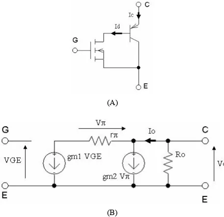
[image:4.595.310.551.352.547.2] [image:4.595.60.295.435.610.2]small signal model that accounts the single device effects.
(A)
(B)
Figure 7. IGBT equivalent circuit (A), small signal IGBT model (B)
Figure 7A shows the typical IGBT equivalent circuit that includes the cascade of the MOSFET and PNP BJT device. If we consider the single device small signal model, we obtain the equivalent circuit reported in Figure 7B, where the single device trans conductance gm1 and gm2 are evidenced. Moreover the model reports the BJT input resistance (rπ) and the respective output one (Ro). The MOSFET output resistance has not been considered because its value is much higher than rπ. We can remember that this model is obtained in the IGBT centre band operation.
By the analysis of the Figure 7.B, the Io current can be calculated as:
π
V
g
V
g
I
o=
m1 GE+
m2 (1)moreover:
GE m
V
g
r
V
π=
π 1 (2) from the (1) and (2), turns out:GE m
m m
o
g
g
g
r
V
I
=
(
1+
2 1 π)
(3)For a BJT device, as a first order approximation, the small signal input resistance can be calculated as:
2
m
g
r
π=
β
(4)whereβ is the BJT static current gain. Replacing (4) in (3) turns out:
GE m
o
g
V
I
=
(
β
+
1
)
1 (5) Moreover the MOSFET trans conductance can be related to the respective currents [10] as:d m
k
I
g
1=
(6) where the drain current can be calculated as:1
+
=
β
cd
I
I
(7)From (5), (6) and (7) turns out:
c GE
o
k
V
I
I
=
(
β
+
1
)
(8) As a final result, the total trans conductance can be calculated as:c GE
o
V
k
I
I
G
=
/
=
(
β
+
1
)
(9) We can remember that the equation (9) goes out from a first order approximation model.The obtained relationship can be used in the model reported in Figure 6 to obtain the trans conductance value, known β value and k MOSFET parameter.
By the analysis of the equation (9), we can observe that the IGBT trans conductance value is related to the collector current by a not linear relationship and its value is determined practically by the MOSFET device. In fact the β
value for the BJT section of IGBT module is very low and the relationship (9) becomes very similar to the MOSFET trans conductance.
6. Frequency Response Simulation
Results
The high frequency IGBT module model reported in Figure 6 can be used to understand and reproduce the high frequency IGBT module behaviour. The low frequency voltage gain dependence from the collector current is directly related to the trans-conductance (G) value that can be calculated using the previously analysis.
[image:5.595.63.291.101.322.2]Figure 8. Output voltage simulation at f = 1MHz and Vin=25mVpp
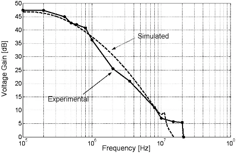
The proposed model allows us to reproduce both the transient and frequency IGBT module behaviour. Figure 8 shows the PSpice simulated output voltage and the respective zoom at f=1MHz and Vin=25mVpp, input signal. The collector current and voltage are Ic=100A and Vce=300V, respectively. The simulated waveforms are very similar to those observed in Figure 2. Moreover the proposed model reproduces very accurately the IGBT module high frequency Bode diagram. Figure 9 shows a comparison between experimental (solid line) and simulated (dotted line) frequency behaviour for a supply voltage of 350V and a collector current of 200A. A quite good accuracy can be recognized. Moreover, from the analysis of Figure 9, we can recognize a peak in the frequency response at about (20MHz) that is quite well reproduced also by the proposed model. This peak seems to be of the same nature of the resonant peaks measured on the same modules [3].
Figure 9. Comparison between experimental and simulated high frequency response
7. Discussions
The experimental and simulation results have demonstrated that the IGBT modules can exhibit very high
frequency voltage gain that can induce very high power gain. These considerations can be useful in the converter design, for EMI reduction. In effect, the IGBT module is the main responsible of the high frequency noise emission in the high power converters [8], which is made more relevant by this amplification phenomena. Therefore, care must be taken for driver design in order to reduce the effects of the power stage voltage gain.
8. Conclusions
The radio frequency behavior of high power IGBT modules has been experimentally characterized. It has been demonstrated that such modules exhibit a significant high frequency voltage gain when they are operated in the active region. A small signal high frequency model has been presented which is able to describe self-sustaining oscillations and EMI emission. The model well describes the high frequency IGBT modules response and could be used in a PSpice simulation to predict the irradiated noise during converter operation, with a reasonable accuracy. Moreover, the model could be used to predict the electromagnetic noise in particular operating conditions, when the IGBT is subject to very high voltage and current values or during short circuit operation.
REFERENCES
[1] C. Martin, J. L. Schanen, R. Pasterczyk: “Inside a Power Module”, Industry Applications Conference, 39th IAS Annual Meeting. Conference Record of the 2004 IEEE, pp. 1519-1525, October 2004.
[image:6.595.108.505.79.267.2] [image:6.595.59.293.503.655.2][3] G. Busatto, C. Abbate, F. Iannuzzo, L. Fratelli, B. Cascone, G. Giannini: “EMI Characterisation of high power IGBT modules For Traction Application” Power Electronics Specialists Conference, 2005, PESC 05, Record 36th, pp. 2180-2186, Recife - Brazil.
[4] A. Domurat-Linde, K.D. Lang, E. Hoene:“Influence of IGBT-module switching characteristics to radiofrequency noise”, EMC Europe, 2012, pp 1-6.
[5] R. J. Valentine: “IGBT High Frequency Operation” Industry Applications Conference, 1996, IAS Annual Meeting, IAS '96., Conference Record of the 1996 IEEE Volume 3, 6-10
Oct. 1996 pp: 1464 - 1471 vol.3.
[6] M. Akhbari, N. Pierre, J. L. Schanen: “Optimisation of Gate Circuit Layout to Suppress Power/Drive Interaction” Thirty-Third IAS Annual Meeting, IEEE Volume 2, 12-15 Oct. 1998 pp.1078 - 1084 vol.2.
[7] PSPICE, Version 9, http://www.orcad.com.