SCIENTIFIC COMPUTATION
E L E C T RON IC ASSOC IA T E S, INC. West Long Branch, New Jersey
8400 SCIENTIF1C COMPUTING SYSTEM
REFERENCE
HANDBOOK
•
I
CONTENTS
CHAPTER 1 - SYSTEM DESCRIPTION . • . . . . • . • . . . • . . • . . . . • . . . • . . 1.1 INTRODUCTION . . . • . . . • . . . 1. 2 EXPANSIONS . . . • . . . . • . • . . . • • . • . • . . . • . . . • . . • . . . 1. 2. 1 8402 Basic Computing System . . . . 1. 2. 2 8403 Basic Computing System . . . . 1. 2. 3 8410 Central Processor . . . . 1. 2.4 8420 Memory Module . . . . 1. 2. 5 8430 Exchange Module . . . • . . . 1. 2. 6 8440 Desk Console . . . • . . 1. 2. 7 8490 Power Module . . . . 1. 3 P R O C E S S O R . . .
1. 3. 1 Memory Word . • • . . . • . . . • . . . . • . . . 1. 3. 2 Instruction Word • . . . • . • . . . • . • • . • . . . 1. 3. 3 Data, Word Formats . . • . . . . 1. 3.4 Processor Registers . . . • . . . . • . . • . . . • . . . 1. 4 ADDRESSING • • • . . . • . . . • . . . . • . . • . . . • . . • . . . . • . . . • • . . . . • . . • . . . 1. 4. 1 Direct Addressing • . • • • • . . • . . . . • . • • . • • • • . • . . • • • • • • . . • . • • . • • • . . 1. 4.2 Indexed Addressing . . • . . • . • . • • • . • . . . • . . . • . • . . . • . . . • . . . 1. 4.3 Indirect Addressing • . . • • . . . • . . . . • . . • . . . • . . . • . . . . • . . . 1. 4. 4 Immediate Addressing • • . • . • . • • . • . . • . • • . . . • • . • • • . • • . . . . • . • . . . 1. 5 INTERRU PT SYSTEM • • . . . • . . . • . . . • • . . . • . . .
CHAPTER 2 - INSTRUCTION REPERTOIRE . . . . 2. 1 INTRODUCTION . . . . 2.2 EFFECTIVE ADDRESS CALCULATIONS . . . . 2. 2. 1 Direct Addressing . . . . 2. 2. 2 Indexing . . . . 2. 2. 3 Indirect AddreSSing . . . . 2. 2.4 Summary . . . . 2.2.5 Combinations of AddreSSing Options . . . . 2. 3 ARITHMETIC INSTRUCTIONS . . . . 2.4 NOTATION . . . . 2.4. 1 Addressing Conventions . . . . 2.4.2 Register Conventions . . . . 2. 5 THE FIXED POINT INSTRUCTION CLASS . . . . 2. 5. 1 The Save Register . . . • . . . 2. 5. 2 The Accumulator Address. . . . 2. 6 THE EXTENDED PRECISION INSTRUCTION CLASS . . • . . . 2. 7 THE INDEX INSTRUCTION CLASS . • . . . 2.8 FLOATING POINT INSTRUCTION CLASS • . . . • . . .
1-1 1-1 1-1 1-3 1-3 1-3 1-4 1-4 1-4 1-4 1-6 1-6 1-7 1-7 1-10 1-12 1-12 1-13 1-13 1-13 1-13
CONTENTS (Cont)
2.8.1 Floating Divide. • . . • . . . • . . . 2-12 2.8.2 Floating Multiply. . . • . . . • . . . • . . • . . . 2-13 2.9 THE DOUBLE PRECISION INSTRUCTION CLASS. . . 2-13 2.10 THE INTEGER INSTRUCTION CLASS. . . 2-14 2.10.1 F l o a t i n g . . . 2-15 2.10.2 Integerizing . . . • . . . , . . . 2-15 2.11 BOOLEAN CONNECTIVE INSTRUCTIONS. . . 2-16 2.11. 1 The Mnemonics. . . 2-17 2.11. 2 A d d r e s s i n g . . . 2-18 2.12 CONDITIONAL INSTRUCTIONS. . . 2-21 2.12.1 The Flag Operations. . . 2-21 2.12.2 Index Jumps XJ, XJT. . . 2-22 2.13 INSTRUCTIONS TO LOAD AND STORE SPECIAL REGISTERS. . . 2-22 2. 13. 1 Load Register or Bus. . . 2-22 2.13.2 Store from Register or Bus. . . 2-23 2.13.3 The Flag Register. . . 2-23 2.13.4 Location Counter. . . 2-23 2. 13. 5 T i m e r . . . 2-24 2. 13.6 Mask Register . . . . • . . . . . 2-24 2.13.7 Console Register. . . 2-24 2.14 EXEC BIT INSTRUCTIONS. . . 2-24 2.14.1 Exec Bit Controls . . . • . . . 2-24 2.14.2 Accumulator Exec Bits. . . 2-25 2.15 INPUT/OUTPUT INSTRUCTIONS. . . 2-25 2. 15. 1 SFL Instruction (Set Function Line) . . . 2-25 2.15.2 TSL Instruction (Test Status Line) . . . 2-27 2.15.3 LDCD, STCD Instructions. . . 2-27 2.15.4 LDCC, STCC Instructions. . . 2-28 2.15.5 LDOB, STIB Instructions.. . . 2-29 2.16 SHIFT, ROTATE AND NORMALIZE INSTRUCTIONS . . . 2-29 2. 16. 1 Arithmetic Shift . . . ... . . 2-29 2.16.2 R o t a t e s . . . 2-30
CHAPTER 3 - PRIORITY INTERRUPT SYSTEM. . . 3-1 3.1 I N T R O D U C T I O N . . . 3-1 3.2 BASIC OPERATION. . . 3-1 3.3 P R I O R I T y . . . 3-1 3.4 INTERRUPT CONTROL. . . 3-3 3.5 MASKING . . . 3-5 3.6 USER/MONITOR MODE AND THE INTERNAL INTERRUPTS. . . 3-6
CONTENTS (Cont)
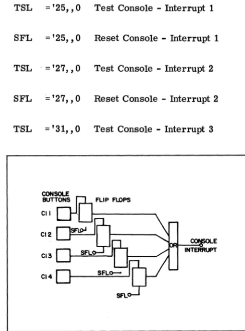
3.7 EXTERNALmTERRUPTS . . . . 3.8 CONSOLE INDICATORS
Page
3-10 3-10
CHAPTER 4 - mpUT/OUTPUT SYSTEM . . . 4-1 4.1 m T R O D U C T I O N . . . 4-1 4.2 DATA CHANNELS. . . .. 4-1
4.2.1 4.2.2 4.2.3 4.2.4 4.2.5 4.2.6
Function Structure
Instructions . . . . Programming . . . . Byte Assembly/Disassembly . . . . Code Conversion . . . .
4-1 4-2 4-4 4-6 4-7 4-8 4.3 AUTOMATIC DATA CHANNEL PROCESSOR. . . .. 4-8 4. 3. 1 F u n c t i o n . . . 4-8 4.3.2 S t r u c t u r e . . . 4-8 4.3.3 Control Words . . . 4-8 4.3.4 Operation . . . 4-10 4.4 SYSTEM INTERFACE . . . 4-11 4.4.1 F u n c t i o n . . . 4-11 4.4. 2 S t r u c t u r e . . . 4-12 4.4.3 SFL/TSL Instructions . . . 4-13 4.5 PERIPHERAL DEVICES. . . .. 4-14 4.5.1 Typewriter . . . 4-14 4.5.2 Card Reader (Models 8452, 8453, and 8454) . . . .. 4-16 4. 5. 3 Paper Tape Reader .. . . . .. 4- 20 4.5.4 Paper Tape Punch . . . , 4-21 4.5.5 Line Printer (Models 8461, 8462, and 8463) . . . .. 4-22 4.5.6 Card Punch (Models 8455 and 8456) . . . 4-26
CHAPTER 5 - COMPUTER CONSOLE OPERATIONS. . . 5-1 5.1 m T R O D U C T I O N . . . 5-1 5.2 CONTROLS AND INDICATORS. . . .. 5-2
5.2.1 5.2.2 5.2.3 5.2.4 5.2.5 5.2.6 5.2.7
Register Controls . . . . Typewriter Input Controls . . . . Exponent Fault . . . . Interrupt Indicators . . . . Channel Condition Indicators . . . . Parity Indicators . . . . System Flag Indicators . . . .
5-2 5-3 5-5 5-5 5-5 5-6 5-6 5.2.8 Programmer Flag Controls and Indicators. . . .. 5-6 5.2.9 Console Interrupt Controls and Indicators . . . . . 5-6 5.2. 10 Configuration Switches . . . .
5.2. 11 AUTO LOAD and AUTO DUMP . . . .
CONTENTS (Cont)
Page
5.2. 12 Clock Controls . . . .. 5-7 5.2. 13 System Controls and Indicators . . . 5-7 5.2. 14 Console Register. . . .. 5-7 5.3 CONSOLE DISPLAY . . . 5-7 5.3.1 Accumulator . . . 5-7 5.3. 2 Display Register . . . .. 5-7 5.3.3
5.3.4 5.3.5 5.3.6 5.3.7 5.3.8 5.3.9
Memory Data
Memory Address . . . . Exchange Assembly . . . . Location Counter
Channel Function . . . . Channel Buffer . . . . . , . . . .. . . . . . Instruction . . . .
5-8 5-8 5-8 5-8 5-8 5-9 5-9 5.3.10 Typewriter Input. . . .. 5-9 5.4 Maintenance Panel. . . .. 5-9 5.4. 1 Lamp Test . . . .. 5-9
5.4.2 Keyboard 5-9
5.4.3 Clock Control . . . .. 5-9 5.4.4 M o d e . . . 5-10 5.4.5 Left Half, Right Half, Left Exec, and Right Exec . . . . . . .. 5-10 5.4.6 PCO, PC1, PC2, and PC3 . . . 5-10 5.4.7 Data Test . . . 5-10 5.4.8 ERR(Error) . . . 5-10 5.4.9 B a n k S e l e c t . . . 5-11 5.4.10 P a t t e r n C o n t r o l . . . 5-11 5.4.11 Memory - LD/NORM/UNLD .. . . . .. 5-11 5.4.12 Clock - STEP/NORM/START . . . 5-11 5.4.13
5.4.14
Channel Select Device Select
5-11 5-11 5.4.15 Byte 4/8 . . . 5-12 5.4.16 EBITE/E . . . 5-12 5.4.17 C o d e - B I N / B C D . . . 5-12 5.4. 18 DBCO, DBC 1, DBC2 . . . 5-12
5.4.19 DSCO, DSC1, DSC2 5-12
5.4.20 CSCO, CSC1, CSC2 . . . 5-12 5.4.21 C1CO, C1C1 • . . . • . . . • . . . • . . • . . . .. 5-12 5.4.22 CCOThroughCC4 . . . 5-12
CONTENTS (Cont)
Page
4. FLOATING POINT NUMBERS . . . . . . .. Al-2 5. INTEGERS. . . .. Al-2 6. ALPHANUMERIC DATA. . . .. Al-2 7. GENERALIZED DATA . . . . . . .. Al-3
APPENDIX 2 8400 INSTRUCTION AND TEST MNEMONICS. . . .. A2-1
APPENDIX 3 - TABLE OF INTERRUPT ADDRESS CODES. . . .. A3-1 1. ANALOG-TO-DIGITAL CONVERSIONS . . . . . .. A3-2 2. OPERATION CODES FOR ANALOG MONITOR/CONTROL . . . A3-2
APPENDIX 4 - TABLE OF SFL/TSL CODES. . . .. A4-1 1.
2.
3.
4.
PROCESSOR INTERRUPT SFL PROCESSOR INTERRUPT TSL EXCHANGE INTERRUPT SFL EXCHANGE INTERRUPT TSL
A4-1 A4-1 A4-2 A4-2 5. HYBRID SFL's . . . . . . .. A4-2
APPENDIX 5 - CHARACTER CODE EQUIVALENCE TABLE . . . A5-1
APPENDIX 6 - POWERS OF TWO . . . • . . . A6-1
APPENDIX 7 - OCTAL-DECIMAL INTEGER CONVERSION • . . . A7-1
APPENDIX 8 - HOLLERITH CARD CODES . . . A8-1
APPENDIX 9 - LINKING LOADER TEXT BINARY CARD FORMAT . . . • . . . A9-1
APPENDIX 10 - PAPER TAPE FORMAT . . . AlO-1
APPENDIX 11 - TWO'S COMPLEMENT ARITHMETIC . . . A11-1 1. THE TWO'S COMPLEMENTS SYSTEM . . . . . . .. A11-1 2. RANGE OF NUMBERS . . . . . . .. A11-1 3. TRUNCATION AND ROUND-OFF. . . .. A11-1 4. SHIFTS. . . .. All-3 5. OVERFLOWS. . . .. All-4 6. MULTIPLE PRECISION . . . .. Al1-4
Figure Number 1-1 1-2 1-3 1-4 1-5 1-6 1-7 2-1 2-2 3-1 3-2 3-3 3-4 3-5 4-1 4-2 4-3 4-4 4-5 4-6 4-7 4-8 4-9 4-10 4-11 4-12 4-13 4-14 4-15 4-16 4-17 4-18 4-19 4-20 4-21 4-22 4-23 ILLUSTRATIONS Title
Typical 8400 Scientific Computing System 8400 System Diagrams . . . . .
Memory Word Format . . . . . Instruction Word Format- . . . . Summary of 8400 Word Format . . . . Processor Registers . . . . Universal Accumulator Formats
8400 Registers . . . . Effective Address Calculation . . . .
Interrupt Register Mask Enable Configuration . . . . Interrupt States . . . . Multi-Level Interrupts . . " . . . .
Internal Interrupt Conditions . Console Interrupt Buttons . . .
Exchange Module . . . . The Elements of a Data Channel . . . .
Data Channel SFL Instructions Data Channel TSL Instructions
Program-Controlled Data Transfer . . . • . . . Byte Size/Byte Count Variation . . . .
Channel Control Word Format . . . . ADC P Action for a TCD Operation . . . . Typewriter Keyboard . . . . Connection of Typewriter to the Channel Buffer Register
Typewriter Character Position in Memory . . . . . . . . Typewriter SFL Codes . . . .
Hollerith- BCD Code on a Card . . . . Position of Binary Card Characters in an 8-bit Byte . . . . Card Reader TSL Codes . . . . Card Reader SFL Codes . . . .
Paper Tape Reader SFL Instructions . . . . Paper Tape Punch SFL Instructions . . . .
Vertical Format Codes . . . .
Line Printer TSL Instructions . . . . Line Printer SFL Instructions . . . • . . . Card Punch SFL Instructions
Card Punch TSL Instructions
Figure Number
4-24 4-25 5-1 5-2
5-3 5-4 5"'-5 5-6 5-7
ILLUSTRATIONS (Cont)
Magnetic Tape SFL Instruction Magnetic Tape TSL [nstruction
Title
Control Console . . . . . . Control Panel . . . .
Register Display/[nput-Output Typewriter . . . < • • • •
Paper Tape Reader and Maintenance Panel . . . . System Control Panel . . . . System Display Panel . . . . • . . . Maintenance Control Panel . . . .
CHAPTER 1
SYSTEM DESCRIPTION
1. 1 INTRODUCTION
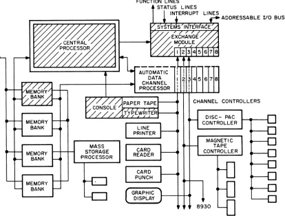
The 8400 Scientific Computing System (Figure 1-1) Organization is made up of three autonomous subsys-tems; memory, processor, and exchange, which operate together from one control. Figure 1-2 illus-trates, in block diagram form, a typical 8400 Scien-tific Computing System.
The memory consists of from one to four banks with individual controls. Each bank has four storage ac-cess channels for multiple acac-cess communication. In the typical configuration shown in Figure 1-2, the first channel of each bank is connected to a bus from the processor. Another separate bus ties together the second channel of each bank. This bus is con-nected to each optional Automatic Data Channel Con-troller used. The banks' third and fourth channels are available for bus connection to external proces-sors and mass memory devices. With this arrange-ment, the banks can be accessed in an over lapped fashion by the central processor and by the external processors in an expanded multiprocessor system. Each bank can also exchange information with exter-nal mass memory devices for efficient time-sharing processes. With this configuration, the processors may continue computation during input/output activity.
The central processor, functioning as the heart of the system, has two-way communication with all subsys-tems and optional Automatic Data Channel Control-lers. Provided with a complete capability of per-forming all required arithmetic and logical operations, it performs the major part in control and execution of the stored program. The achievement is accom-plished by an accumulator and an extensive comple-ment of registers, control lineS, and logic circuitry. In general, the basic items of this subsystem are: logic signal control, status lines, function lines,
in-terrupt lines, special control registers, location counter, interval timer control, instruction register, flag register, high-speed save register, and seven index registers including the Universal Accumulator.
The last subsystem, the exchange, consists of a data channel control system and a system interface. The data channel control system provides a fully buffered interface with external input/output (I/O) devices. It includes up to eight two-way data channels which can be controlled by either the program or one of the optional Automatic Data Channel Controllers. Each channel has the capability of controlling up to fifteen external devices. The system interface includes an I/O bus system that is directly addressable, as well as provision for status control lines, function control lines, and external interrupt lines; as required for the integration of hybrid or other systems with the 8400.
Two additional units, the Automatic Data Channel Controller and the console, are shown separately in the diagram. The first of these, an optional expan-sion in the exchange, provides data channel control for data transfer (independent of processor opera-tion) between external devices and memory. The console, which is considered as part of the proces-sor, includes: system controls, register displays, an on-line typewriter and a paper tape station.
1. 2 EXPANSIONS
MEMORY BANK
MEMORY BANK
MEMORY BANK
MASS STORAGE PROCESSOR
FUNCTION LINES STATUS LINES
INTERRUPT
I I
I I
~r45678 I
I
CHANNEL CONTROLLERS
DISC- PAC CONTROLLER
MAGNETIC TAPE CONTROLLER
[image:12.612.115.529.53.367.2]8930
Figure 1-2. 8400 System Diagrams
a brief outline of the basic systems (8402, 8403) along with the standard and optional components available. Figure 1-2 illustrates the various configu-rations.
1. 2. 1 8402 Basic Computing System - Includes the following:
8410 Floating Point Processor;
8420 Memory Module - 8K capacity;
8430 Exchange Module;
8440 Desk Console;
8490 Power Module.
1. 2. 2 8403 Basic Computing System - Same as the 8402 System except that the memory module has a 16K storage capacity.
1. 2. 3 8410 Central. Processor - Including:
Hardware for performing fixed and floating pOint arithmetic;
Three high-speed index registers and four in-dex registers in coret;
Masked priority interrupt system with 16 in-ternal. and 16 exin-ternal. levels;
Power fail-safe system;
Exchange module (8430) with one (8431) data channel, one (8440) desk console with on-line input-output typewriter and one (8490) power system;
Indirect, immediate and byte addressing capa-bility; and, SAVE register with 560 nanosecond cycle time.
Masked priority interrupt system with 16 internal and 16 external levels; and
Power fail-safe system tied to the highest interrupt level.
1. 2. 4 8420 Memory Module - Includes:
Core storage capacity of 8192 words, each con-taining 32 bits for information, 2 EXEC bits for special control functions and 2 parity bits;
A 650 nanosecond access time;
A 1. 75 microsecond cycle time;
Independent read/write control enabling over-lapped operations with other memory banks; and,
The capability for handling independent busses from up to four request sources.
Maximum one unit to be added in field.
1. 2.5 8430 Exchange Module - Includes:
A channel control system that can accommo-date up to eight 8431 data channels;
Two bi -directional buffered data channels each capable of handling 16-bit parallel communica-tion;
The capability for handling 15 device control-lers per channel;
The capability for controlling 16, 8 and 4-bit byte assembly or disassembly sequences, in-cluding parity checking or generation as well as conversion of BCD to processor collating codes;
The capability for independent channel control from the processor or from the optional, 8435-1 Automatic Data Channel Control System
(per-An availability for four channel interrupt lines when less than five 8431 data channels are used;
A systems interface with up to 16, fully-buffered, 16-bit parallel input/output busses - up to 128 groups of status lines with 8 lines per group -and up to 128 groups of function lines with 8 lines per group; and,
Interface terminations for optional external priority interrupt system expansions, for up to 256 interrupt levels.
1. 2.6 8440 Desk Console - Including:
Operator's panel with complete display and control facilities including console, status line control and processor access for on-line pa-rameter changing;
A maintenance panel;
An on-line, Selectric Typewriter for manual and program -controlled input/output.
1. 2. 7 8490 Power Module - Including:
A capability for providing the 8400 system's full power requirements;
Provisions for the manual, marginal testing of memory;
Provisions for power-fail monitoring; and,
Provision for over/under power protection.
1. 2. 8 The follOWing list includes optional pe-ripheral devices and system expansion components:
8441 Paper Tape Station - with a 500 cps read and 110 cps punch capability. (cps = Char/sec).
8417 Timer Register - provides addressable, real-time millisecond clock.
8422 8K Memory Bank - with same features as 8422-E Memory Module. (Maximum four banks per 8400.)
8423 16K Memory Bank - with a 16,384 word, core storage capacity; other features are the same as those for the 8420 Memory Module. (Maximum four banks per 8400. )
8431 Program Control Data Channel - provides a data channel capability for any exchange module channel position, from 1 to 7; handles up to 15 peripheral device controllers.
84351 Automatic Data Channel Processor
-provides independent block data transfer con-trol for the 8431 data channel of channel posi-tion 0 in the exchange module; requires the use of an 8420 Memory Interface Pak; independent of central llrocessor.
8435-2, 3, 4 Automatic Data Channel Proces-sor Expansions - each adds independent block data transfer control for one 8431 data channel occupying any channel position between 1 and 7 in the exchange module; 8435-1 Automatic Data Channel is required in order to use the expan-sion. (Maximum of three. )
842021,22,23,24 Memory Interface Pak
-provides coupling interface between 8435-1 Automatic Data Channel Processor and Memory Banks 1, 2, 3, anli 4, respectively. Maximum of four; one required per memory bank. Neces-sary if an ADCP is to be used.
8437-2 through 16 External Interrupt System Expansion Group - each group adds 16 inter-rupt lines to basic external interinter-rupt system.
8438-1 through 128 Status Line Package - pro-vides in the exchange additional status line groups of 8 lines each (two 8-line groups per unit). Each package provides fully buffered
flip-flop storage for sense input from external devices .. (Maximum 64 groups.)
8439-1 through 128 Function Line Package
-provides in the exchange additional function groups of 8 lines each (two 8-line groups per unit). Each package provides fully buffered flip-flop storage for function line output to ex-ternal devices. (Maximun 64 groups.)
8441 Paper Tape Station - 500 character-per-second read and 110 character-per-character-per-second punch. Mounting provisions are included in the
8440 Central Console.
8452 Card Reader - 400 cards-per-minute; 12 row cards, 80 column read.
8453 Card Reader - 800 cards-per-minute; 12 row cards, 80 column read.
8454 Card Reader - 1400 cards-per-minute; 12 row cards, 80 column read.
8455 Serial Card Punch - 100 cards-per -minute to 316 cpm.
8456 Parallel Card Punch· 300 cards-per-minute.
8461 Line Printer - 300 lines-per-minute; 132 columns-per-line, 64 characters, buffered
printer.
8462 Line Printer - 600 lines-per-minute; 132 columns-per-line, 64 characters, buffered
printer.
8463 Line Printer - 1000 lines-per-minute.
8472 Magnetic Tape System - provides con-troller handlin up to four transports (8473); one is included, maximum of four. The
tape transport uses 7 -track, IBM compatible tapes and operates at 45 ips and 556 and 800 bpi, respectively.
one is included (maximum of four). The tape transport uses 7 -track, IBM compatible tapes and operates at 75 ips and 556 and 800 bpi, respectively.
8476 Magnetic Tape System - provides con-troller handling up to four transports (8477); one is included. The tape transport uses 7-track, IBM compatible tapes and operates at 120 ips and 556 and 800 bpi, respectively.
8478 Magnetic Tape System - provides con-troller handling up to four transports (8479); one is included. The tape transport (8479) uses 7-track, IBM compatible tapes and oper-ates at 150 ips and 556 and 800 bpi, respec-tively.
NDTE
8481 Display Monitor - provides point, line and character plotting on a 10" x 10" display of 1024 points along each axis. Light pen is included.
1. 3 PROCESSOR
1. 3.1 Memory Word
The 8400 Computer's memory word 'consists of 36 bits: 2 bits for parity check, 2 bits for program control (EXEC bits), and 32 data bits. The memory word format is shown in Figure 1-3.
Model Numbers 8472-9, 8474-9, 8476-9, and
The parity bits are generated and stored on a half-word basis during the write cycle. Parity is then checked during the read cycle. If an error is lo-cated, the console indicator lights and a parity inter-rupt
J!3
initiated. The 8400 System uses odd parity; this means that whenever the number of logic ONE's8478-9 are the same as the models listed above
except that they use 9 track IBM compatible tapes.
0 151 16
INFORMATION
16-BIT HALF-WORD
I
32-BIT FULL -WORD
,
8-BIT BYTES
I·
4-BIT BYTESI I I I II
I I I
H,T BYTES11111111111111111,·"
T BYTES31 32 33 3435
16-BIT HALF-WORD E E P P
making up a word is even, a parity bit is generated so that the result is odd. (Using odd parity, the parity bit is always the opposite when all l's or O's are used.)
The EXEC bits, in effect, expand the system's soft-ware capability. Used by the programmer to tag selected memory words, these two bits are also capable of the following:
enabling interrupt control for memory protection,
dynamic relocation of object programs,
. .. stack or table pOinting, and so forth.
EXEC bit control is discussed in Chapter 2.
The information portion of the word may contain a full (32-bit) word, two half (16-bit) words, or por-tions thereof (8, 4, 2, or 1-bit) for Boolean operations.
1. 3. 2 Instruction Word
Instructions are executed in sequence by the 8400 Instruction Register (I). Each instruction has a 32-bit word format as shown in Figure 1-4. This figure
0 15
M FIELD
16
*
indicates the normal program control capabilities of the instruction word; for example, addressing, ad-dress modification, and instruction interpretation. The first sixteen bits (M field) in the word format represent the operand address during a data fetch. It may also signify: an instruction address during an instruction fetch, an immediate operand, or a shift count. The next four bits designate any address modification required. If bit 16 (*) is a binary 1, the M field contains the address of another location in memory that will replace the present M field, rather than the address of an operand. Bits 17 through 19 (X, where X = 1 to 7) specify the number of an Index register. Either or both may be used to change the interpretation of the instruction address during execution.
The last 12-bit (OP field) portion of the word format denotes the operation to be performed.
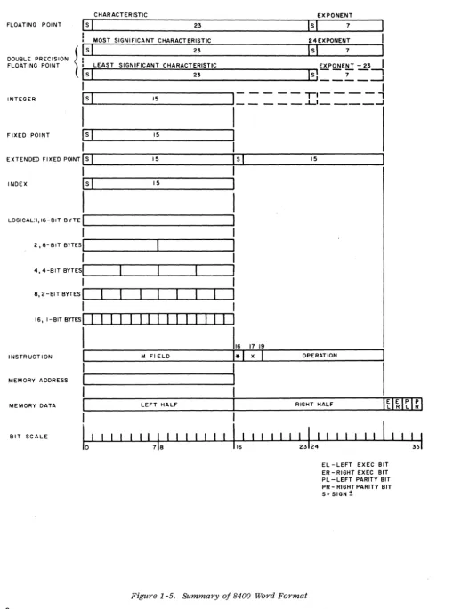
1. 3. 3 Data Word Formats
This section describes the word formats used in the 8400 Computer. The brief descriptions refer to Figure 1-5. Arithmetic formats are in a two's complement notation with the + sign (binary 1) indi-cating a negative quantity. The instruction, memory data and memory address word formats are included in Figure 1-5 for comparison.
17 19 20 31
X OP FIELD
M 16 - BIT (MEMORY) ADDRESS FIELD
*
I - BIT INDIRECT ADDRESS MODIFIERX 3 - BIT INDEXING MODIFIER
FLOATING POI NT
DOUBLE PRECISION FLOATING POINT
INTEGER
CHARACTERISTIC
S
I
23MOST SIGNIFICANT CHARACTERISTIC
{
sl
LEAST SIGNIFICANT CHARACTERISTIC 23sl
~~s ...
I _____
1_5 _ _ _ _ _ ---', _ _I
FIXED POINT
~s
....IL...---1_5---~1
I
EXPONENT
lSi
724EXPONENT
lsi
7,
EXPONENT - 23
I
Isl==7
=:J
I
-- ,-1----'
_ _ _ -1-1 _ _ _ _ ....1
15 EXTENDED FIXED POINT
I
SI
15 SI
I~---~---~
INDEX IS I
I~---'
15LOGICAL: I, 16-BIT BYTE
I
I~---~
2, a-BIT BYTESI~ _ _ _ _ _ _ "'--_ _ _ _ _ _ ~
4, 4-BIT BYTESI
I~-~--~--~-~
16, 1- BIT BYTES
1
II I 1 1.1 I 1 I 1 1 1 I 1
INSTRUCTION M FI ELD
MEMORY ADDRESS
MEMORY DATA LEFT HALF
BIT SCALE
I II
7 a
6 17 19
16
OPERATION
RIGHT HALF
ItlMrl~1
EL - LEFT EXEC BIT ER - RIGHT EXEC BIT PL - LEFT PARITY BIT PR - RIGHT PARITY BIT
[image:17.620.44.553.55.740.2]1. 3. 3.1 Floating-Point. Floating-point num-bers are either single word (32-bit), or double pre-cision (56-bit) quantities. The single-prepre-cision floating-point number consists of:
•.. a fractional part (23 magnitude bits),
a sign bit,
and an exponent part ( 7 magnitude bits)
with its own sign bit.
This single-precision floating-point notation provides an accuracy of six.decimal digits.
The double-precision floating-point number occupies two consecutive memory word locations .. The word with the lowest address contains the most significant fraction and exponent bits. The signed exponent part of the word (eight bits) with the higher address is
. . 23
adJusted durmg memory store to EXP-2 . Double floating-point notation provides an accuracy of thir-teen decimal digits.
The double-precision floating-point word format has direct correspondence with the single floating-point format. For example, when executing a 32-bit floating-point multiply, the product will be in the double-precision word format. Therefore, the re-sults of several 32-bit floating-point multiply opera-tions can be accumulated using double-precision floating-point add operations. The results may be operated on individually since the sign and exponent for each of the most significant and least significant portions are preserved.
Floating-point operations are normalized (adjustment of the mantissa and floating-point number so that the mantissa lies in the prescribed normal range) auto-matically after each operation unless the instruction is post-modified by the unnormalized symbol (U). Normalization is accomplished by using left shifts to remove all leading zeros from the number in the accumulator. The shifting continues until the con-tents of the first two bit positions (0, 1) in the
accu-1. 3. 3. 2 Fixed-Point. Formats for the stan-dard (16-bit) and extended (32-bit) fixed-point quan-tities are illustrated in Figure 1-5. The standard fixed-point format consists of a 15-bit fraction along
.'
with a sign bit and may occupy either half-word position of the memory word. The extended fixed-point format contains two 15-bit fractional parts
and a sign bit for each. Its left half-word contains the fifteen most significant bits and the sign of the entire 30-bit fractional quantities, In standard fixed-pOint arithmetic operations, the half-words are addressed individually.
1. 3. 3. 3 Integer. Integer arithmetic instruc-tion involve operainstruc-tions with two types of data words:
1. Standard, 16-bit fixed-point and
2. Single, 32-bit floating-point.
The data word associated with the system memory is standard, 16-bit, fixed-point notation. The operand in the Accumulator is in single 32-bit, floating-point notation. In the integer mode, a 16-bit, fixed-point number is automatically converted from the half-word memory location to the floating-point format.
LikeWise, a floating-point number in the accumu-lator which represents the result of a series of floating-point operations, is integerized and stored in the designated half-word memory location. Opera-tions in this mode may be either normalized or unnor-malized by post modifying the associated instructions.
1. 3.3. 4 Index. In this operation, the contents . of a specified index register is arithmetically combined
with the contents of a half-word memory location. The result, obtained in the accumulator, is automati-cally transferred back into the specific index regi-ster and the previous contents of the accumulator ar! restored.
byte positions, logical connective and recipient (either memory or accumulator) of the operation results.
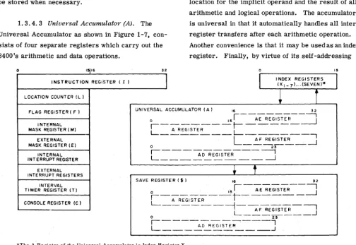
1. 3. 4 Processor Registers
The following registers in the 8400 Computer provide the major portion of the Processor's capability for control and execution of the stored program. (See Figure 1-6).
1.3.4.1 Instruction Register (l). This 32-bit register stores each instruction as it is executed. The register format is the same as the 8400 instruc-tion word as shown in Figure 1-4.
1. 3. 4.2 Location Counter (L). This 16-bit register contains the address of the next instruction to be loaded into the Instruction Register. Its primary function is to provide system program control by se-quentially directing the flow of instructions into the system. The contents of the Location Counter may be stored when necessary.
1. 3. 4. 3 Universal Accumulator (A). The Universal Accumulator as shown in Figure 1-7, con-sists of four separate registers which carry out the 8400's arithmetic and data operations.
o I 16 32
INSTRUCTION REGISTER ( r 1
I
LOCATION COUNTER (L 1
The first section, the 16-bit A Register, is used by itself for 16-bit fixed-point operations and as the most significant 16 bits of all other operations. The second section, the AE Register, is used when ex-tended fixed-point and exex-tended shift operations are needed. It enables the A Register to Handle 32-bit fixed-point quantities such as: 32-bit, double-length products; and dividends of standard, 16-bit fixed-point multiply and divide operations. The AF Regis-ter, the third section, is a 16-bit A Register exten-sion and is used for single-word (32 -bit) floating-point quantities. The final section, the AD Register, provides a 24-bit extension to the AF Register. This enables the accumulator to handle 56-bit,
precision floating-point quantities; such as the double-precision products and dividends of a single-word floating-point multiplication and division operations.
The accumulator provides several special 8400 pro-gramming features. It provides a single refere.nce location for the implicit operand and the result of all arithmetic and logical operations. The accumulator is universal in that it automatically handles all inter-register transfers after each arithmetic operation. Another convenience is that it may be used as an index register. Finally, by virtue of its self-addressing
o 15
I
INDEX REGISTERS (X I _7) .. ·(SEVEN)*~
i
FLAG REGISTER ( F 1 UNIVERSAL ACCUMULATOR (A) 16 32
INTERNAL MASK REGISTER (Ml
EXTERNAL MASK REGISTER (El
INTERNAL INTERRUPT REGISTER
EXTERNAL INTERRUPT REGISTERS
INTERVAL TIMER REGISTER (Tl
CONSOLE REGISTER (C 1
o 151--A~REG~ER--=-=:]
, t
-A REGISTER
L _ _ _ _ _ _ _ _ L- _ _ _ _ _ _ _ -,
L
AF REGISTER ~-0 23
, - - - -
---,
L _ _ _ _ ~D~E~~.:mR _ _ _ ~
~
f
SAVE REGISTER ($ I .6 32
, - - - ,
o 15 A E REGISTER
'-~REGI-;:;:-E_;_---I-_ _ _ _ _ _ ---1
L- _ _ _ _ _ _
--j _ _ _ _ _ _
--,
L_~~GIST~ _ _ ..J
0 23
, - - - l
L _ _ _ ~D~~S~R _ _ _ _ ..J [image:19.623.37.542.357.704.2]16 17 31
s I
r~---0 I 15 AE REGISTER
~ S I MANTISSA (CONTINUED IN AF REGISTER)
..J .!..M~T.!!'!.N ~I ~~ ~R!.. W!!E!! ~E~ W..!.T~ ~ ~G~T~R
A REGISTER 16 23 "24 31
(CONTINUATION I
_ _ _ O!,. ~N~'~A:' _
-1 ___
E~P~~T _ _ _ _AF REGISTER
MANTISSA (LEAST SIGNIFICANT PART)
- - - -AD
REGISTER - - --Figure 1-7. Universal Accumulator Formats
capability, the accumulator enables the performance of doubling and squaring at high speeds. This self-addressing capability also enables data transfer be-tween the accumulator and all index registers. The Universal Accumulator is addressable as memory location zero.
1. 3. 4.4 Save Register ($). The Save Register
is a high-speed storage register similar to the Universal Accumulator. (See Figures 1-6 and 1-7.) This register is used to retain the entire contents of the accumulator prior to the execution of any arith-metic or shift instruction. The Save option is de-signated by the & symbol and may be used with any 'arithmetic or shift operation.
The programmer, by using the Save Register, is able to store or read operands in 560 nanoseconds, less time than it takes using core memory. The data is automatically arranged in the proper format when recalled by the Universal Accumulator. Similar to a memory cell, this register retains data until a subsequent instruction containing the $ symbol stores new data; the data is NOT destroyed during the save-write cycle.
1.3.4.5 Index Register (X1- 7). Seven index registers including the Universal Accumulator (index register one) provide automatic address modification. These registers retain ha:lf-word numbers that are
When indexed address modification is specified, the effective address is formed by adding the contents of the selected index register to the contents of the M field. This operation has no effect on index register content.
Index arithmetic instructions allow direct operation between the respective contents of a specified index register and an addressed memory location. A single instruction effects the following: An automatic parallel transfer of the contents of the addressed index register to the Universal Accumulator; an arithmetic operation, as specified, combining this quantity with that contained in the addressed memory location; and, an automatic transfer of the result back to the same index register. The transfer from the index register is made to the parallel A Register of the Universal Accumulator with the previous A Register contents being stored. Since the index register has no extension (AE Register), its use is restricted to operations giving a half-word (16-bit) results.
Tested by a set of transfer operations, the flags pro-vide the basis for the 8400's extensive program-control capability. They signify modifications of the normal sequential control for the program. Basic control instructions affected include the following:
HJf
EXf
Lf
LRf
Jf
JRf
JSf
HALT if flag f set and JUMP when execute button depressed;
EXECUTE instruction at specified location if flag f set;
LINK to subroutine if flag f set;
LINK to subroutine if flag f set, RESET flag; JUMP if flag f set;
JUMP if flag f set;
JUMP if flag f set, RESET flag;
JUMP if flag f set, SET flag;
JTf JUMP if flag f set, TRIGGER flag.
The LINK and JUMP operations are conditional; they depend upon the status of the flag tested. The setting, resetting, or triggering (complementing) of the flag, however, is unconditional.
The Flag Register bits indicate the status of 16 inter-nal machine conditions. Eight of the bits serve as programmer console flags and are set by either con-sole switches or the program. Internal machine status conditions can be preserved at any particular time by storing the entire register contents in mem-ory. This enables the programmer to retrieve inter-nal machine status after the occurrence of subsequent interrupt conditions.
1. 3. 4.7 Mask Registers, Internal (M) and External (E). The Internal Mask Register and Ex-ternal Mask Register permit the programmer to select the interrupts a program will respond to and, to es-tablish a priority- among these interrupts. These l6-bit registers are loaded and stored by the use .of
1. 3. 4.8 Console Register (C). This l6-bit register enables monitoring, data display and data input while the program is in progress. It may be loaded by the operator or by the program..
1. 3 .. 4.9 Interval Timer Register (T). Enabled by the LOAD INTERVAL TIMER (LDT) instruction, this l6-bit register decrements one count each milli-second t providing computer real-time control. As the register goes through zero, an interrupt is gen-erated and the register is reset to its maximum value. At this point, unless reloaded by the interrupt subroutine, the register continues to decrement as before.
With all its bit positions occupied, the Interval Timer. Register will decrement through a maximum time
range of 65,
~36-l milliseconds{~2n)InterruPts
may\\n=o
be programmed to occur at any selected' time interval within this range. Consequently, the register is extremely useful for: program synchronization, periodic output of data, time-sharing programs or consoles, periodic sense line testing, and many other purposes.
1. 4 ADDRESSING
The extensive addressing capability in the 8400 Scientific Computing System facilitates the handling of all normally encountered address manipulations in-volving core memory locations. Direct, indexed, and indirect addressing have been made available to the programmer •. In addition, an immediate or literal addressing capability provides programming flexi-bility for fast efficient processing.
1. 4. 1 Direct Addressing
With direct addressing, the l6-bit address specified
used in the specified operation. In arithmetic opera-tions, either full-word or half -word operands may be used. With full-word operands, the entire contents of the specified memory location are involved. With half-word operands, either the right or left half of the full-word location is used. The half-word to be used is designated in the instruction by a / (slash) post modifier (see Chapter 2).
For double precision arithmetic operations, the con-tents of both the specified memory location and the next memory location (M + 1) are accessed. In Boolean operations, the specific half-word (including its byte size and position) is specified by using post modifiers in the associated instruction, i. e. , AHM4/ SAM,,3. In this instruction: 4 specifies a four-bit byte; SAM designates the memory location and, being to the right of the slash, the right half-word of this full-word location is specified. The instruction states, "where each of the four bits in the third byte position are high, set the corresponding bits in the right half-word of memory location SAM".
1.4.2 IndexedAddressing
Indexed addressing represents an important and highly useful variation of direct addressing. The 8400 contains seven index registers providing an . efficient, flexible means of address modification.
Indexing adds the contents of an index register to the address portion of an instruction, Bits 17, 18, and 19 of the instruction word specify which one of the seven index registers is to be activated. If bit posi-tions 17, 18, and 19 are zero, no indexing is speci-fied. The contents of anyone of the computers' seven index registers are added to the 16-bit address field (base part) to form the "effective address".
1. 4. 3 Indirect Addressing
Multi-level indirect addressing may· be used without being restricted by any 8400 instructions. The
*
bit (bit 16) of the instruction word is used as the in-direct indicator. When inin-direct addressing isspeci-where the address of the data may be found. Thus, the address of the data is given indirectly.
If both an index register and indirect addressing are
.'
required by the programmer, the effective address is computed as previously discussed and then the in-direct address is computed.
1. 4. 4 Immediate Addressing
The 16-bit address of an arithmetic or logical in-struction serves as the operand when immediate addreSSing is used. This operand is a signed number represented in two's complement notation. Immedi-ate addressing is specified in the 12-bit operation (OP) field of the instruction word and is accomplished in symbolic notation by placing the = symbol in this field.
This form of addressing saves instruction time since it permits the direct use of data from the Instruction Register; no memory access required. This form of addressing also saves memory space since no operand memory locations are required and; in ad-dition, the operand may be modified by the contents of a specifiC index register since the immediate operand is located in the instruction word address field. With this modification accomplished prior 'to using the immediate operand, the effective immediate
operand concept can be used by the programmer to provide greater programming flexibility.
CA
store command with immediate addressing capability is called an NOP.)The immediate operand notion extends to shifting operations as well. In a SHIFT instruction, the desired number of shifts is speCified as an arithme-tic operand. Direction of shifting is determined by the shift count sign. And, as an immediate operand, this shift count may be modified by the contents of a specified index register.
1. 5 INTERRUPT SYSTEM
con-without a loss of return-continuity. When an internal or external interrupt condition occurs and the inter-rupt action is not inhibited by masks, an instruction in a reversed interrupt location is executed (each interrupt condition has a reversed location). The execution of this instruction does not change Location Counter contents. LINK, the normally executed instruction, transfers control to the interrupt routine while preserving the return address of the interrupted program. Once started, an interrupt action may be interrupted by the occurrence of a subsequent sys-tem interrupt condition.
The interrupt system responds to internal conditions and operating modes monitored by sixteen internal interrupt lines. It is also responsive to any of up to
256 external conditions monitored by an expanded complement of external interrupt lines. There are 16 external interrupt lines in the first group with a capability of up to 15 additional external groups. The complete system is arranged in 17 groups containing 16 individual interrupt levels apiece. Group 0 in-cludes the internal interrupt levels and groups 1 through 16, the external interrupt levels. Each group
has priority over the succeeding group and each group level over lower levels.
Basically, 16 flip-flops (each set by a particular interrupt condition) are scanned. A scanner will accept a flip-flop output only if the Interrupt Enable bit in the Flag Register and the corresponding mask register bit are both high. The scanner begins scan-ning at selected points in the instruction flow, con-tinues until an interrupt condition is detected, and then locks onto that position. The priority of a scanner is established when no "higher-priority" scanner has locked up. Mter priority has been established, interrupt logic determines the address of the reserved interrupt location.
CHAPTER 2
INSTRUCTION REPERTOIRE
2. 1 INTRODUCTION
This chapter contains a complete and precise defini-tion of the operadefini-tions performed by every 8400 instruction. Further details on input/output in-structions for peripheral devices are given in Chapter 4. The emphasis in this chapter is on pro-gramming rules and conventions; moreover, as an aid in learning the entire repertoire, the instruc-tions are presented in classes and sets. The pro-gramming conventions and notation used are taken from the 8400 Macro-Assembler manual (EAI Publication Number 07 800.0001-3). The actualOP code numerical values are given in the appendix and in the 8400 Programmer's Card.
Consistent with the objective of presenting the in-struction repertoire as the programmer will use it, the view of the computer is offered as functional -appropriate for the programmer. Therefore, Figure 2.1 illustrates the essential programmable elements of the central processor. Only the 16-bit input and output busses are missing. The registers required for momentary storage of data traveling to the ac-cumulator from the memory is only one explicit inter-register transfer and that is between the ac-cumulator and the Save ($) Register. The memory-to-register transfer paths are obvious; therefore, not shown. Other register transfers which are closely related to the instruction and their options are developed in the text below.
Figure 2.1 illustrates the following important facts:
• •• The Save Register can hold a copy of the accumulator contents except for the exec bits (shown crosshatched);
· •• the EA and AF Registers are alternative extensions of the A Register;
· •• the A Register is also treated as Index
.•• the instruction address field in the left portion of the instruction word;
••• other special registers are a half-word in size.
2.2 EFFECTIVE ADDRESS CALCULATIONS
2. 2. 1 Direct Addressing
All instructions referencing an operand in memory specify one of several ways to address the operand. The most basiC, direct addreSSing, uses the 16-bit left hand number of the instruction word as the operand address. Other addressing modes are termed: index modification, indirect addressing, and immediate addressing. Half-word addreSSing, a variation on each of the above, is allowed when the operand is a 16-bit word. The left or right half-word selection is made after a memory address. This left/right option is an integral part of the OP code (bits 20 to 31 of the I Register as shown in Figure 2.1).
2. 2. 2 Indexing
One of the primary uses of index registers arises from their ability to modify instruction addresses. For this to occur, the instruction must specify the particular index register that is to take part in the modifying activity. Indexing adds the contents of an index reg-ister to the address portion of an instruction.
When indeXing is speCified, the contents of the index registers are added algebraically, in two's comple-ment notation, to the address portion of the
instruction. This new address, the effective address, is then to be used as the operand.
INDEX REGISTERS
o 15
X7 X6 X5 X4 X3
PROCESSOR REGISTER X2
o
T
c
REGISTERE M
F
L.
o I. I. 52 I ....
1 __
m_--1.JH_x ...
1 _op_-,
o M ORY II
EI IE
8400 REGISTERS
Figure 2.1
As an example of address modification, assume that memory address 500 contains the instruction AD 124,2 and this instruction has a two in the appropriate index register position. If the contents of the index regis-ter are 27, then the number stored in memory loca-tion 151 (124 + 27
=
151) is added into the accumu-lator when the add AD instruction is executed. Note that memory location 500 still contains the instruction AD 124,2 in its original form. Memory address 151 is called the effective address, and the process is called address modification; that is, the address of the instruction is modified in the central processor for execution purposes, but is unaltered in memory.2.2.3 Indirect Addressing
When proceSSing data is located in several different areas of memory, it is at times convenient to operate upon an indirect address as opposed to an actual ad-dress. For example, if the programmer wishes to perform an add instruction at memory location 3000
(assume that memory location 123 already contains
AD 123.
However, if he wishes to add to the accumulator, not the contents of memory location 123 but the contents
of the contents of memory locat:i.on 123, then the
com-puter would add the contents of location 1862 to the accumulator. This procedure is known as indirect addressing, and occurs when a 1 is placed in bit position 16 (*) of the instruction word. Mnemonically, it is written as:
AD* 123
Note that if an index register and indirect addressing
are requested by the programmer, the effective ad-dress is computed as previously discussed and then the indirect address is computed.
2.2.4 Summary
Table 2.1 lists the entire 8400 Instruction Repertoire.
An instruction that has a number (m) in the left half-word and no address modifier in the right half-half-word
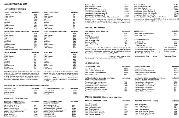
8400 INSTRUCTION LIST
ARITHMETIC OPERATIONS 32·BIT FLOA TING.POINT
Subtract Cleor Subtract Cleor Add
Add
Com pore
Multiply
Store Store Rounded Divide Clear Divide
MNEMONIC FSB FCS FCA FAD FCP FMP FST FSR FDV FCD 56·BIT DOUBLE FLOATING.POINT MNEMONIC
Subtract DSB
C lear Subtract DeS
C lear Add DCA
Add DAD
Comparet DCP
Multiply l' DMP
Store OST
Store Round"cI t DSR
Divide t DOV
Clear Divide t OeD
t denotes compatible subroutine operat;ons
16·BIT INTEGER MNEMONIC
Subtract ISB
Clear Subtract ICS
Cleor Add ICA
Add lAD
Compare ICP
Multiply IMP
Store 1ST
Stor. Rounded ISR
Divide IDV
Clear Divide ICD
Operation modifiers extend the basic list. The post modifier "U" specifies unnormaHzed operation for F,D and f Classes. The premodifier "$" specifies a Scive Register store of the accumulator contents prior to the execution of a modified instruction of any class. Examples: FADUi SEAD or $FADU.
Table 2.1. 8400 Instruction Repertoire
16·BIT FIXED POINT
Subtract Clear Subtract Clear Add
Add Compar.
Multiply Store Store Rounded Divide Clear Divide
32·BIT EXTENDED FIXen.POINT
Subtract Clear Subtract Cleor Add
Add
Compore t MultlplYf
Store Stor. Rounded t Divide t Clear Divide t 16·BIT INDEX
Subtract C lear Subtract Cleaf Add
Add
Compare Multiply Store Store Rounded Divide Clear Divide
MNEMONIC SB CS CA AD CP MP ST SR DV CD MNEMONIC ESB ECS ECA EAD ECP EMP EST ESR EDV ECD MNEMONIC XSB XCS XCA XAD XCP XMP XST XSR XDV XCD
The prefixes or suHixes in the mnemonic symbol denote the class of operation or operation condi-tions. The basic symbol indicates t"'e operation itself.
ElI:ample: In FAD, F stands for Floating.Point Arithmetic (32·bit precision). AD indicates the ADO operation.
Both Low (Nor) Both Different (Excl Or) Both Same (Equiv) Complement Both High (And A)
Complement Either High (Or A)
Complement Either Low (Nand A)
Complement Both Low (Nor A)
Byte Equality Test (Set Z Flag if Bytes identical)
BLAn BDAn BSAn CSHAn CEHAn CELAn CBLAn BECTn Example: ELAn specifies that the result of a NAND, with on n .. bit byte in A and an n.blt byte in M, replace the A.byte. T"'e mnemonic: is interprered as follows: "For corresponding bit positions in t"'e
CONTROL OPERATIONS TEST BRANCH _ ON "FLAG". I
Holt - Jump Execut. Link (To Subroutine) Link _ Res.t Flag Jump _ Trigg.r Flag
Jump - Set Flog Jump _ Reset Flag Jump MNEMONIC HJI EXI LI LRI JTI JSI JRI JI
f denotes one of the 16 conditions monitored by a special flag register. T"'ese conditions are listed below with their respective mnemonics. Complement conditions can be specffied by prefixing the condition mnemonics with the modifier, tiN".
Examples: Halt Jump on Over· flow Is coded HJV. Holt Jump on no Overflow Is HJNV.
1/0 OPERATIONS
1/0 REGISTER LOAD
Load Output BU55 Load Channel Dota Register Load Channel Control Register Set Function Line
AUTOMATIC DATA CHANNEL CONTROL _ DATA BLOCK TRANSMISSION
MNEMONIC LDOS LOCD LDCC SFL MNEMONIC
SHIFTING, ROTATION AND NORMALIZING OPERATIONS
Transmit on Count _ Disconnect Transmit Until Signal _ Disconnect Transmit on Either _ Disconnect Transmit on Count _ Interrupt Transmit Until Signal _ Interrupt Transmit on Either _ Interrupt
TCD TSD TED TCI TSI TEl ACCUMULATOR
Arithmetic Shift Logical Rotate Normalize
LOGICAL BYTE OPERATIONS BOOLEAN CONNECTIVES _ RESUL TS TO ACCUMULATOR
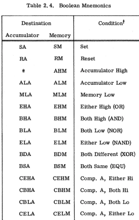
Set (A 11 Ones in A) Reset (Ail Zeros in A) Memory High (Load M) Accumulator Low (Complement A) Memory Low (Complement M) Bot'" Hig'" (And)
MNEMONIC ASH ROT NRM MNEMONIC SAn RAn MHAn ALAn MLAn BHAn
EXTENDED ACCUMULA TOR
Arit"'metic Shift Logical Rotate Normalize
BOOLEAN COt.NECTIVES _ RESULTS TO MEMORY
Set (All Ones in M) Reset (All Zeros in M) Accumulator High (Store A) Accumulator Low (Complement A) Memory Low (Complement M) Both High (And)
MNEMONIC EASH EROT ENRM MNEMONIC SMn RMn AHMn ALMn MLMn BHMn
SPECIAL REGISTER TRANSFER OPERATIONS REGISTER TRANSFER _ LOAD
Load A -Extended Load Flag Register Loai Locotion Counter Load Timer Register Load Mask Register Internal Load External Mask Register
MNEMONIC LDAE LDF LDL LOT LDM LOE
Both Low (Nor) Both Different (Exel Or)
Both Same (Equiv) Complement Both High (And A)
Complement Either High (Or 'A'>
Complement -Either Low (Nand A)
Complement Both Low (Nor A)
Memory High (Set Z Flag if Byt. in M is Zero)
BLMn BDMn BSMn CBHMn CEHMn CELMn CBLMn MHMn A·byte and the _~byte,where EITHER the A.bit or the M .. bit is LOW. set resultant A.bit. n= 1,2,4,8 or 16 bits.
INDEX JUMPS
Index Jump - Unconditional Index Jump Test
EXEC BIT CONTROL
Set EXEC Bit Reset EXEC Bft Test EXEC Bit Accumulator Equals Zero Accumulator Greoter than Zero Accumulator Less than Zero Overflow (Cumulative) Unconditionally True blank
I/O REGISTER STORE
Store Input Buss Storoe Channel Doto Register Store Channel Control Register Test Stotus Line
Z G L V MNEMONIC XJ XJT MNEMONIC SEX REX TEX
Carty (Or Borrow) C Busy Data Channel B Enabled Interrupt E
Progrommer Flags 1·8
MNEMONIC STiB SlCD STCC TSL AUTOMATIC DATA CHANNEL CONTROL _
NO DATA BLOCK TRANSMISSION
MNEMONIC
Skip on Count _ Disconnect Skip Until Signal _ Disconnect Skip on Either _ Disconnect Skip on Count _ Interrupt Skip Until Signol _ Interrupt Skip on Either _ Interrupt
REGISTER TRANSFER _ STORE
Store A Extended Store Flag Register Store Location Counter Store Timer Register Store Mask Register Internal Store Externol Mask Register
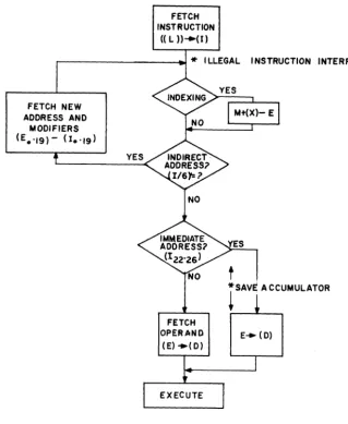
[image:26.799.59.744.98.551.2]specified, the number (m) is "immediately" treated as data (operand) rather than as an address. If the Indirect option is specified, core memory address m contains the "address" of the operand rather than the operand itself. If the Index option is specified, a number is taken from one of the seven index regis-ters and added to m to produce the effective address of the operand; while the left half contents (m) re-main the same. Several options may be used simul-taneously as described in the following section. In any case, the action of address modification is often referred to as "effective address calculation". Since this is a common occurrence and is possible with the majority of instructions, the E notation is used regularly throughout for the contents of the effective address.
2.2. 5 Combinations of Addressing Options
The various address modifiers and the legal combi-nations thereof are shown in Table 2.2 in the format used when writing instructions for the assembler.
The precedence of the addressing options is: X, *, =, or
I.
This means that index modification (X)takes place before indirect addressing (*), and the final option is the half-word selection of immediate, left, or right (= and
I
cannot appear simultaneously). This sequence is illustrated in Figure 2.2. The nota-tion in this figure is that parentheses around a regis-ter name specify the regisregis-ter contents; the arrow reads as "replaces", and subscripts indicate specific register bits.The flow diagram of Figure 2.2 is interpreted as
follows:
1. The instruction cycle starts with an instruction fetch, which is denoted as
«L»-
(I), or "The contents of the memory address that is the contents of L replaces the contents of the instruction register, I".2. If indexing is speCified (by 1 to 7 in bit positions 117, 18, 19) then the sum of the number m in the instruction address field and the contents of the specified index register forms (tenta-tively) the effective address E.
Table 2.2
Modifier Name Format Remarks
* Indirect Address OPN* M The address for the given instruction is taken from the ad-dress portion of the 32-bit word at location M. Multiple indirect addressing is possible. All instructions may use an indirect address.
X Address Modification OPN M,x The effective address is obtained by adding the contents of the speCified index register, X, to the address, M. That is, M + (X) - E .A. All instructions except the Index Register Class can have address modification. Indexing precedes in-direct addressing at every level if both are specified.
I
Halfword Address OPN /M The operand for 16-bit operations comes from the left half of M by usingMI
and the right half of M by using1M.
The slash (/) has no effect on indexing or indirect addressing. A 16-bit operation written OPN M is interpreted by the Assem-bler as OPNMI.
= Immediate Address OPN=M The operand for this instruction is taken from the address field of the instruction itself. The immediate address may not be used with
I.
The immediate address is applicable to all 16-bit operations except Store and Store After Rounding.REMARKS: All legal combinations of the address modifiers are illustrated below:
OPNMI
OPNM
OPN/M
OPN M/ ,X OPN
1M,
X OPN* M!OPN*
1M
OPN*M/,x
OPN*IM,X
OPN=M OPN = M,X OPN* = M
FETCH INSTRUCTION
(( L
» ....
(1)I LLEGAL I NSTRUCTION INTERRUPT
FETCH NEW ADDRESS AND
MODIFIERS (E.· 19 )- (1.'19)
FETCH
OPERAND
(E) ~(O)
rSAVE ACCUMULATOR
E-+ (D)
[image:28.632.161.480.50.438.2]EFFECTIVE ADDRESS
CALCULATION
Figure 2.2
3. If indirect addressing is specified (by 116
=
1) then a new word, located atad-dress E, is obtained from the memory. Only the first 19 bits of this word are used, and they replace the contents of bit I o:19 ' Now, the original value m has been re-placed in I by (EO:15)$ and the index and
indirect bits have also been replaced. Steps 1, 2, and 3 are repeated until for some indirect address, indirect addressing is not specified. It is possible, through a programming error, for the above loop to be a closed path, which "hangs-up" the computer. Such a loop can be broken only
by a manual halt or an interrupt. However, in the normal course, indirect references can be made (at the expense of time for each memory fetch) and indexing (for dif-ferent index registers) can be performed at each level of indirectness.
used as the effective memory address for the final gathering of data from the mem-ory. After this gathering, the left/right option selects the specified half-word for execution.
5. Note that the Save option takes place just after the immediate address test on either path.
The different effective address calculations may be specified as follows, where OPN signifies any operation code for which the address options are valid.
OPNm
OPNm/
OPN/m
OPN m, X
OPN /00, X
tOPN*m
tOPN*/m
tOPN*m, X
tOPN*/m, X
OPN=m
OPN= 00, X
operand = (E0:15) or (E
o:
31 )' E=
00operand = (E0:15)' E = 00
operand = (E 16:31)' E = 00
operand = (E0:15) or (E
o:
31 )' E=m+(X)operand = (E 16:31)' E = m+ (X)
operand = (E
o:
15 ) or (Eo:
31 )' E= (00)operand = (E16:31)' E = (00)
operand = (E 0:15) or (E 0:31)'
E = (m + (X»
operand = (E 16:31)' E =
(m + (X»
operand = E = 00 (16-bit operand only)
operand = E = 00 + (X) (16-bit operand only)
tOPN*=m
OPN*= m, X
operand = E = (m) (16-bit operand only)
operand = E = (m + (X» (16-bit operand only)
2.3 ARITHMETIC INSTRUCTIONS
There are ten basic arithmetic instructions that occur in each of six classes of operation. The classes differ in the form of arithmetic, word size, and the registers affected. The resultant sixty mnemonics and their functions are readily committed to memory. There are numerous variations to these basic instructions and they follow a consistent and logical pattern. All arithmetic instructions may exercise the Save option prior to execution; and they set Z, G, and L decision flags after execution. All floatillg-point operations may terminate with an un-normalized result. All multiply and divide operations require double length registers, hence the double preCision instructions are executed by subroutines. These mnemonics (and some others in the set of sixty basic operations) are recognized by the assem-bler and replaced by the appropriate Link instruction. Alternatively, the actual codes for these instructions are recognized by the computer and cause an interrupt
(number 2 interrupt). Software is provided
to
select the right subroutine. All compare, store, and store-rounded instructions leave the entire accumulator unchanged. The add, subtract, and store-rounded conditions generally result in bit (C) of the flag register being set. The carry flag (C) indicates that an arithmetic 'carry has been produced. Divide con-ditions can result in setting the overflow (V) flag (see Paragraph 2.8.1).2.4 NOTATION
2. 4. 1 Addressing Conventions
E
(E)
m
IE,
1m
effective adQress
contents of E
contents of address field of instruction word
specifies right half-word for 16-bit operands
E,
E/,
m, ml speCifies left half-word for 16-bit operandsOP= m
OPm,X
OP*m
OP* m,X
immediate address, m is a literal, a constant
indexing, X is an integer 1 to 7;
E
=
m + (X) except Index Class instructionsindirect addressing, E
=
(m)indexing plus indirect, E
=
(m + (X))(Note: the
*
is part of the OP field)2.4.2 Register Conventions
(A)
(AAE)
(AAF)
(AAFAD)
($)
contents of the 16-bit A Register of the Accumulator
contents of the Extended Fixed-Point Accumulator
contents of the Floating-Point Accumulator
contents of the Double Preci-sion Accumulator
contents of the Save Register
($A)
($AAE)
($AAF)
($AAFAD)
(AD 0, 9:23)
int( )
Jrac( )
contents of the 16-bit A portion of the Save Register
contents of the Extended Fixed-Point Save Register
contents of the Floating- Point Save Register
contents of the Double PreCi-sion Save Register
contents of bits 0 to 7 in A Register
contents of bits 0 and 9 to 23 in the AD Register
the one's complement of the contents of 0 to 7 of A
left Exec bit at effective address
right Exec bit at effective address
Accumulator Exec bits
the integer part of the floating-point operand. Note that for two's complement numbers the integer part is always the most positive integer that is more negative than the number, hence for negative numbers the magni-tude of the integer part is larger than the magnitude of the number.