Technology (IJRASET)
©IJRASET 2015: All Rights are Reserved r
229
Computer-Aided Analysis for Device Modelling
Of 45nm MOSFET
Susidra S1, Thiruvalar Selvan P2
1
PG scholar, M.E VLSI Design, TRP Engineering College (SRM Group) 2
Associate professor, Department of ECE, TRP Engineering College (SRM Group)
Abstract— The present scenario of the MOSFET device scaling has resulted in severe short channel effects and transport degradation. In addition, variability in deeply scaled transistor such as threshold voltage Vth variability has emerged as a
major challenge for circuit and device design. MOSFETs with deeply retrograde channel profile requires higher and higher substrate doping’s to control short channel effects. The depletion width of the MOSFET scales down, the substrate doping that determines the threshold voltage and also controls the short channel effects. The design of the deeply retrograde channel MOSFET with the gate length of 45nm and the drain to source channel length of 32nm are designed. The device simulation is carried out using the energy balance model with SILVACO TCAD tool.The design of the MOSFET is determined by the characteristic of drain current, gate to source current input and output voltage of transistor are obtained using 1.2V using HSPICE software.The main novelties related to the 45nm technology such as gate oxide, metal gate, low interconnect dielectric are implemented in the MICROWIND tool and the characteristic of subthreshold swing, comparison of current and voltage are determined by layout simulation.
Keywords— Retrograde channel profile, Short channel effects, Threshold voltage, doping region, low surface.
I. INTRODUCTION
The Metal-Oxide Semiconductor Field Effect Transistor (MOSFET) is largely regarded as a popular device and is extensively used in digital circuits, microprocessors, memory circuit, and other logic applications of many kinds. This is due to the MOSFET ability to act as an efficient switch that practically consumes no current at the gate and the channel conductivity dependents only on the potentials at the gate. The relatively small size of the MOSFET causes millions of devices that can be fabricated into a single integrated circuit design is another advantage to the electronics industry [1].The deeply retrograde channel profile and the low surface doping which gives potential to lower threshold voltage variability [2].The short channel effect can be overcome by lowering the doping surface by gate length of 45nm.
MOSFET device performance is mainly determined by carrier transportation in the channel. The gate contact is separated from the channel by an insulating silicon dioxide (SIO2) layer [4]. The charge carriers of the conducting channel constitute an inversion charge, that is electrons in the case of p-type (n-channel device) or holes in the case of an n- type substrate (p-channel device). NMOS transistors are faster than their PMOS counterpart and more of them can be put on a single chip. A MOSFET device is considered to be short when the channel length is the same order of magnitude as the depletion layer widths of source and drain junctions. As the channel length L is reduced to increase both the operation speed and the number of components per chip, the so called short channel effects arise [5].The short channel effects are attributed to two physical phenomena: the limitation imposed on the electron drift characteristics in the channel, and the modification of the threshold voltage due to the shortening channel length. The doping profile is called retrograde substrate. The higher doped region prevents the extension of the drain electric field through the lower part of the depletion region, where the gate field is weak. The lower doped region at the surface helps to prevent unacceptable increase in the threshold voltage and to prevent channel mobility reduction that would be caused by higher surface doping. Deeply retrograde channel profile file can be used on bulk platform and has low surface doping.
II. DEVICE STRUCTURE
©IJRASET 2015: All Rights are Reserved r
230
allowable magnitude. It is used to overcome numerical ringing in the calculated potential when bias steps are large (greater than 1V for room temperature calculations).The second method limits the number of linearized Poisson solutions per Gummel iteration, usually to one. This leads to under-relaxation of the potential update. [image:3.612.148.464.289.519.2]To overcome the short channel effect (SCE) the channel length and the gate length is reduced. The channel length modulation in a MOSFET is caused by the increase of the depletion layer width at the drain as the drain voltage is increased [7]. Higher electric fields at the surface as typically obtained in scaled devices push the electron wave function even more into the oxide yielding a field dependent mobility. As devices are reduced in size, the electric field typically also increases and the carriers in the channel have an increased velocity. However at high fields there is no longer a linear relation between the electric field and the velocity as the velocity gradually saturates reaching the saturation velocity. This velocity saturation is caused by the increased scattering rate of highly energetic electrons, primarily due to optical phonon emission [4]. This effect increases the transit time of carriers through the channel. In sub-micron MOSFETs one finds that the average electron velocity is larger than in bulk material, so that velocity saturation is not quite as much of a restriction as initially thought. Hot electrons refer to high energy electrons, which enter the oxide layer and trapped, that will affecting the oxide, to rise to oxide charging [6]. It accumulates with time, and degraded the performance of the device by increasing the threshold voltage, affects its conveyed conductance, and affects adversely the gate’s control on the drain current.
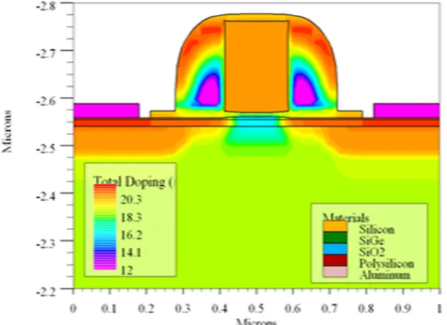
Figure 1. Process simulated device structure for deeply retrograde channel profile
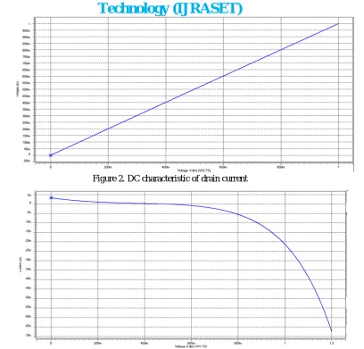
III. DC CHARACTERISTIC USING HSPICE
Technology (IJRASET)
©IJRASET 2015: All Rights are Reserved r
[image:4.612.116.524.58.449.2]231
Figure 2. DC characteristic of drain current
Figure 3. Characteristic of gate to source voltage
III. DESIGN RULE OF 45nm MOSFET USING MICROWIND
The physical mask layout of any circuit to be manufactured using a particular process must conform to a set of geometric constraints or rules, which are generally called layout design rules. These rules usually specify the minimum allowable line widths for physical objects on-chip such as metal and polysilicon interconnects or diffusion areas, minimum feature dimensions, and minimum allowable separations between two such features [11]. If a metal line width is made too small, for example, it is possible for the line to break during the fabrication process or afterwards, resulting in an open circuit. If two lines are placed too close to each other in the layout, they may form an unwanted short circuit by merging during or after the fabrication process.
The main objective of design rules is to achieve a high overall yield and reliability while using the smallest possible silicon area, for any circuit to be manufactured with a particular process. Note that there is usually a trade-off between higher yield which is obtained through conservative geometries, and better area efficiency, which is obtained through aggressive, high- density placement of various features on the chip. The layout design rules which are specified for a particular fabrication process normally represent a reasonable optimum point in terms of yield and density. It must be emphasized, however, that the design rules do not represent strict boundaries which separate “correct” designs from “incorrect” ones.
©IJRASET 2015: All Rights are Reserved r
[image:5.612.155.458.127.355.2]232
polysilicon layer. The NMOS gate is capped with the specific silicon nitride layer that induces lateral tensile channel strain for improved electron mobility. The layout simulation analyze the switching performances in the high speed and low leakage as shown in Figure 4.Figure 4. Layout of 45nm MOS technology
The layout simulation result in which the starting time of the pulse range is 4.50v, the rise and the fall time tends to 0.250v. The clock time ranges as 0.045v as shown in Figure 5. By simulating the 45nm technology we obtain the characteristic of drain current and voltage which attains the saturation region as shown in Figure 6. The gate to source voltage which gradually increases at 0.1v by varying the gate voltage from 0 to 0.5v as shown in Figure 7. The Threshold voltage which attains the value ranges from 0.10 to 0.40v with the length of 0.45 as shown in Figure 8.
[image:5.612.126.522.462.682.2]Technology (IJRASET)
©IJRASET 2015: All Rights are Reserved r
233
[image:6.612.115.542.67.458.2]Figure 6. Characteristic of ID versus VD
[image:6.612.109.544.489.676.2]Figure 7. Characteristic of ID versus VGS
©IJRASET 2015: All Rights are Reserved r
234
In this paper, the threshold voltage of lower surface doping of a deeply retrograde channel profile was simulated by an SILVACO TCAD tool in the existing system. The drain induced barrier lowering is sensitive to drain and source extension. The devices are then characterized by comparing the gate length of 45nm. Several characteristics have been carefully observed. The characteristic of drain current, gate to source current input and output voltage of transistor are obtained using 1.2V using HSPICE software are determined. The 45nm technology such as gate oxide, metal gate, low interconnect dielectric of the Layout simulation are implemented in the MICROWIND tool.REFERENCES
[1] Arora, N., -“MOSFET Models for VLSI Circuit Simulation”, Springer Verlag,1993
[2] Baker. R.J. CMOS – (2005) Circuit Design, Layout, and Simulation. USA: John Wiley & Sons Inc.
[3] Chandan kumar sankar, - “Technology computer aided design”.
[4] Brian Swahn and Soha Hassoun- (2006) Gate Sizing: FinFET vs. 32nm Bulk MOSFETs, Tufts University Medford, 2006
[5] Department of Electrical Engineering, Arizona State University. New Generation of Predictive Technology Model for Sub-45nm Design Exploration-
IEEE, 2000
[6] Department of Electrical Engineering Arizona State University- Predictive Technology Model for Nano-CMOS Design Exploration; pp. -516, 511,
2001
[7] Etienne sicard, Syed Mahfuzul Aziz- Introducing 45nm technology in MICROWIND 3, 2005
[8] F. Babarada, E. Lakatos, M. D. Profirecscu, C. Amza, E. Manea, N. Dumbravescu, 0. Profirescu- “mosfet process optimization and characteristics
extraction”
[10] HSPICE RF Tutorial, Version X, 2005