Catalyst-dependent morphological evolution by
interfacial stress in crystalline
–
amorphous core
–
shell germanium nanowires
†
Nithin Devarajulu Palavalli,aAlireza Yaghoubi,bChih-Chung Lai,aChin-Che Tin,cd Ali Javey*eand Yu-Lun Chueh*a
Directing the morphological evolution of one-dimensional materials in order to tune their properties for a variety of practical applications in optical sensing and solar cells is an ongoing effort. Here, we establish a systematic method for exerting control over the morphology of nanowires (NWs) grown via a vapour–solid–solid (VSS) process from different metal catalysts. We use germanium, a technologically important material, to demonstrate how catalysts influence the axial growth rate of a crystalline core against the lateral vapour deposition of an amorphous shell which in turn deforms the NWs into straight, tapered or spiral geometries due to interfacial stress. Finite element method (FEM) and molecular dynamic (MD) simulations are further utilized to confirm the proposed mechanism of deformation in crystalline–amorphous core–shell NWs.
Introduction
The quantum size effect is sensitively dependent on the shape of nanostructures.1,2As a result, in recent years, considerable effort has been put toward understanding the detailed mech-anism of growth and control of the morphology of nano-materials. The specic technique that is employed for controlled synthesis and growth at the nanoscale can greatly vary based on the precursors as well as the intended applica-tion. For example, methods for directing the growth of nanocrystals by defect-induced secondary nucleation in iono-covalent materials3 or enthalpy-specic plasmatic environments for materials which exhibit strong poly-morphism have been recently reported.4 From a practical standpoint, morphological modications in NWs are particu-larly of interest.5 In several studies, the improved anti-reective properties due to the gradual reduction of the effective refractive index from the tip to the base of NWs have
been shown to signicantly differ for distinct morphologies.6–8
Owing to their superior compatibility with the current fabri-cation techniques, silicon (Si) NWs have been a natural choice for nanoelectronic applications,9,10although Si-based devices
because of the relatively large band gap of Si (Eg 1.12 eV) suffer from poor responsivity in IR and NIR regimes where most transmission bands operate. For this reason, more recently, germanium (Ge) NWs have been studied as a poten-tial replacement for Si NWs as the active material of nanoscale photodetectors operating at telecommunication frequen-cies.11,12With regard to other applications, especially in elec-tronics, Ge due to its substantially higher mobility13and larger excitonic Bohr radius, which enables a more prominent quantum size effect14 is a far more desirable candidate for
high-performance devices.
However, both Si and Ge in their crystalline form are indirect band gap semiconductors and therefore do not effi -ciently absorb light at near band gap energies where phonon and photon (to conserve momentum and energy, respectively) need to simultaneously couple in order to give rise to a strong optical absorption. Meanwhile, it has been suggested that since a-Si does not essentially require a phonon interaction given its lack of long-range order, crystalline–amorphous core–shell Si NWs may have remarkable potential for improvement of absorption.15We have also previously repor-ted black Ge on exible substrates based on crystalline– amorphous core–shell NW arrays with minimal optical reectance (<1%) even for high angles of incidence (75) and relatively short lengths (1 mm).16 Interestingly, Ge NWs
grown in our previous study using nickel (Ni) as catalyst exhibited a tapered structure unlike the completely straight Ge aDepartment of Materials Science and Engineering, National Tsing Hua University, 101
sec 2, Kuang-Fu Road, Hsinchu 30013 Taiwan, Republic of China. E-mail: ylchueh@ mx.nthu.edu.tw
b
Centre for High Impact Research, University of Malaya, Kuala Lumpur 50603, Malaysia
cMaterials Engineering Program, Department of Mechanical Engineering, University of
Malaya, Kuala Lumpur 50603, Malaysia
dDepartment of Physics, 206 Allison Laboratory, Auburn University, AL 36849, USA eDepartment of Electrical Engineering and Computer Sciences, University of California
at Berkeley, Berkeley, CA 94720, USA. E-mail: [email protected]
†Electronic supplementary information (ESI) available: Complementary TEM micrographs show the temperature- and time-dependent growth of NWs. Additionalgure as mentioned in the text. See DOI: 10.1039/c5ra00888c
Cite this:RSC Adv., 2015,5, 28454
Received 15th January 2015 Accepted 2nd March 2015
DOI: 10.1039/c5ra00888c
www.rsc.org/advances
PAPER
Published on 02 March 2015. Downloaded by University of Malaya on 27/04/2015 02:36:18.
NWs in earlier reports where gold (Au) was the catalyst.17The tapering effect in the case of Ni-catalyzed growth was hypothesized16to originate from the difference in the radial vapour deposition rate (a non-catalytic process) and the axial growth rate (a catalytic process governed by the NiGe system phase diagram), but the underlying mechanism of catalyst-dependent morphological evolution in crystalline– amor-phous core–shell NWs has never been systematically exam-ined. Most studies to date particularly deal with growth factors such as temperature, pressure or substrate and their effect on the orientation of NWs.18Manipulating the growth direction
and taking advantage of crystallographic defects allows the development of complex morphologies via kinking and branching. However in the case of individual NWs, rather than hierarchical structures that are produced by branching, there are still contradicting views as to whether stacking faults originate the formation of kinking sites. The only systematic approach in this regard is that of Dick et al. who have demonstrated controlled kinking by insertion of an axial heterojunction based on island growth at the NW–catalyst interface in certain compositions.19
In this paper, we employ Ni, Au and iron (Fe) thinlms as catalyst to grow Ge NWs with tapered, straight, spiral, and ring type morphologies. Experimental results are used to elucidate how tuning the axial rate of growth (Ra)versusthe lateral rate of deposition of the amorphous layer (Rl) which in some cases can be asymmetric, leads to a wide range of stress-induced geometries. FEM simulations based on the modied Stoney's formula for thin lms and more accurate MD calculations considering the non-uniform mist strain distribution in the core–shell structure are also presented to conrm the proposed mechanism of deformation. The model established here can serve as a groundwork for development of engineered crystalline–amorphous core–shell NWs with promising appli-cations in solar cells,20non-volatile crossbar switches,21and
high-capacity battery electrodes.22Other relevant systems that
may benet from the model presented here, are metal-catalyzed Si–Ge core–shell heterostructures that have a similar growth behaviour and have been recently used to demonstrate 1D hole gas systems at room temperature.23
Interfacial stress in these systems are also expected to enable band gap engineering that renders our work even more relevant.24
Experimental section
Initially a thin oxide layer was thermally grown on a silicon substrate. The metal catalyst thinlm (Au30 nm, Ni0.5 nm or Fe100 nm) was then deposited on the oxide layervia thermal evaporation. Ge NWs were grown using GeH4 (12 sccm, 10% balanced in H2) as the precursor at a temperature range of 270–300 C and pressure of 40–50 Torr. The nano-structures were examined by high-resolution transmission electron microscopy (HR-TEM, JEM-3000F, JEOL operated at 300 kV with point-to-point resolution of 0.17 nm) and element mapping was achieved by electron energy loss spectrum (EELS).
Results and discussion
A number of studies have demonstrated the feasibility of growing NWs through either VSS or vapour–liquid–solid (VLS) processes.25,26 and more recently using supercritical-uid–
liquid–solid (SFLS) methods.27 Morales and Lieber28 have
reported Ge NWs from FeGe seeds at 820C using VLS growth. In the present work in contrast, a low-temperature VSS growth at300C was employed in order to enable the use of polymeric substrates for exible devices. Other than practical consider-ations, the low temperature provides an interesting environ-ment for the growth of NWs. We have previously shown that the diameter of the crystalline core of NWs consistently expands with the growth temperature (also see Fig. S1†).16 This behaviour can be attributed to an increase in size of XGe (X: metal catalyst) seeds at higher temperatures prior to axial growth and therefore in principle applies to any catalyst as also reported in earlier studies.15,17Hence, we can conclude that the
growth mechanism behind the crystalline core in core–shell NWs is essentially a catalytic process while the rate at which the axial growth of the amorphous shell takes place, directly correlates with the properties of the intermediate binary phase.29A low growth temperature means that beyond a critical thickness of a few nanometres, the insufficient thermal energy can no longer sustain a VSS-assisted epitaxial growth and the strictly vapour–solid deposition of the amorphous shell dominates in the lateral direction. With the assumption that the direct vapour–solid deposition does not involve a catalytic process, we carried out several experiments to see how tuning the rate of axial growth and that of lateral deposition can be used to guide the evolution of NWs. As shown in the optical and scanning electron micrographs of Fig. 1, the NWs grown using Au catalyst (Fig. 1a) do not exhibit any signicant morpholog-ical deformation whereas those grown viaNi catalyst have a
Fig. 1 Optical micrographs along with the corresponding scanning electron images of different NW morphologies at a temperature of 280C with a pressure of 40 Torr: straight NWs grown using Au (a), tapered NWs grown using Ni (b), and ring-like as well as spiral NWs grown using Fe (c–e).
tapered geometry (Fig. 1b). The case of Fe-catalyzed growth (Fig. 1c) is more interesting as the Ge NWs seem to have a tendency to bend either completely to give rise to ring type morphologies (Fig. 1d) or in a sinusoidal manner to create spiral structures (Fig. 1e).
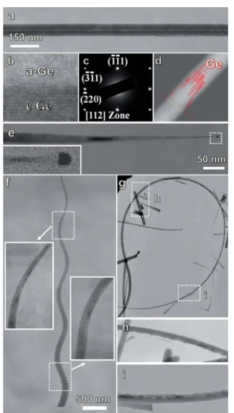
A closer inspection using transmission electron microscopy (TEM) is depicted in Fig. 2. Fig. 2a indicates the core–shell conguration of the Ge NW grown from Au as the catalyst. The corresponding high-resolution TEM image of core–shell Ge NW as shown in Fig. 2b reveals that there is an amorphous shell layer along with a crystalline core made of pure Ge conrmed by selected area electron diffraction (SAED) pattern and energy
dispersive X-ray (EDX) line scan as shown in Fig. 2c and d, respectively. Unlike the Au-catalyzed NWs which have a straight crystalline core, in the case of tapered Ge NWs grown using Ni at the catalyst, the core is considerably smaller with the increased length but at its widest point (at the base) has the same diam-eter as that of the NiGe seed shown in the inset of Fig. 2e. The Fe-catalyzed NWs on other hand mostly consist of a very thick amorphous shell. For spiral NWs, the shell deposition appears to uniformly alternate with the axial growth (Fig. 2f) whereas in the ring type structures (Fig. 2g), the amorphous layer (signied by wrinkles) is asymmetrically present only on the inner side along the ring (Fig. 2h and i). We can therefore categorize the morphology of NWs in terms of the catalytic axial growth rate (Ra) and the non-catalytic vapour–solid lateral deposition rate (Rl). With Au as the catalyst, the low eutectic point of AuGe alloy30promotes a faster axial growth as compared to the lateral deposition rate (Ra[Rl). Therefore, the NWs show no signif-icant deformation. In Ni-catalyzed growth, the rate of catalytic growth is much slower than the rate of lateral deposition (RaRl) because of the high melting point of NiGe alloy and the Ge NW tapering depends on slight differences in growth orientation regardless of the temperature and as a result, the crystalline core is considerably smaller than the amorphous shell. In the case of Fe on the contrary, due to the intermediate melting point of FeGe which is between those of NiGe and AuGe, the Ge NWs have a nearly equal catalytic growth and lateral deposition rates (RaRl), hence the formation of spiral and complete ring morphologies.
It has to be emphasized here that explaining the kinetics of growth for different alloy seeds in terms of relative melting points is not against the proposed VSS mechanism. As Gamalski and colleagues30 have also argued, the system of AuGe for example follows the more kinetically accessible path to form a liquid at very low temperatures (based onin situobservations at 240C), whereas speaking from a thermodynamic standpoint, there should not be a favourable path involving liquid below 360C (based on free-energy calculations for Au–Ge systems). They have concluded that kinetically-driven supersaturation determines the catalyst phase during the growth process. The reaction may start as a VLS-like growth with a metastable liquefaction of Au nanoparticles, however for most of the process it follows a VSS-type process and complete the reaction under solid–solid conditions rather than liquid–solid, hence the general analogy of VSS.
Overall, formation of different morphologies can be attributed to stress relaxation between the amorphous shell and the crys-talline core. To support this notion, one can apply the standard Stoney's formula31to study the stress deformation in core–shell structures, for which the stress bearing of a thinlm with uniform thicknesshfover a substrate of thicknesshscan be dened as
sðfÞ¼ Eshs2k 6hfð1vsÞ
where the stresss(f)of thelm depends on the curvaturekwhile
nandE, which are the Poisson's ratio and Young's modulus, respectively. The subscripts s and f represent the substrate and Fig. 2 TEM micrographs of different morphologies show the
crystal-line–amorphous core–shell structure. Straight NWs grown via Au catalyst exhibit a large crystalline core (a). The corresponding high-resolution TEM (b) and the SAED pattern (c) indicates an interplanar spacing of 3.2 nm attributed to the (111) growth direction. The EDX line (d) confirms the consistent composition of core–shell NWs. (e) The NWs grown using Ni as catalyst with a tapered structure and the NiGe seed (inset) are depicted. NWs grown from Fe thinfilm can either show spiral (f) or ring-like (g) morphologies. The latter is attributed to the asymmetric deposition of the amorphous layer on the inner side as signified by wrinkles (h and i).
[image:3.595.54.283.207.610.2]thin lm, respectively. However, this approach will not bear sufficiently reliable results for this particular case. Based on our observations, we have established that neither the assumption of thickness uniformity nor the equibiaxial in-plane stress are valid due to the intricate morphology. Furthermore, in the standard Stoney's formula, both shear stress and out-of-plane stress are not accounted for, a drawback which adds to its unreliability in our case.
Fortunately, in recent years, great progress have been made with regard to improving the original Stoney's equation by taking into account the minor effects that become increasingly more relevant in complex structures.32–36Freund and Suresh37 have proposed a modied equation for non-uniform substrate andlm curvatures, which can be written in cylindrical coor-dinates as
sðfÞ¼ Eshs2k 6hfð1vsÞ
d
drðkrrþkqqÞ
[image:4.595.332.505.189.333.2]This modied equation provides a method for estimating the crystalline–amorphous interface shear stress with the radial gradient of the sum of the core and shell curvatures (kS¼krr+kqq) andCOMSOL Multiphysicswas used to assess the stress-induced deformation in NWs based on the modied equation.38 Fig. 3a–c show that thenite element model is in good agreement with the interfacial stress mechanism implied earlier from the experimental results. As expected, the straight NWs grown using Au-catalyzed VSS do not undergo any interfacial stress owing to the uniform coating of the amorphous shell layer around the crystalline Ge (Fig. 3a) while the tapered and spiral geometries
clearly present residual stress due to their specic core–shell conguration (Fig. 3b and c). Although the FEM models account for the stress-induced curvature at the core–shell interface, they still do not represent the ratio of the laterally deposited amor-phous shell against the axially grown crystalline core. Therefore, to offer a better insight into the process of deformation at the atomic scale, we need to apply a more comprehensive tool. Feng et al.have lately developed a new approach which expresses the stress gradient s(f)rr + s(f)qq for the non-uniform mist strain distribution corresponding to the non-uniform thickness of the core and the shell as39
sðfÞ
rr þs
ðfÞ
qq ¼ Es 31vs2
hf
8 <
:hs2kS 1vs
2 h
2 skS
þ 1
2 ðR
r½ð13vsÞkSðhÞ 3ð1vsÞkDðhÞhs2ðhÞh
0
sðhÞ
hs0 dh
1vs
R2
ðR
0
h2½k SðhÞ
kDðhÞhs2ðhÞ
h0
sðhÞ
hs0 dh
9 = ;
Similarly, the magnitude for this gradient is determined as
sðfÞ
rr s
ðfÞ
qq ¼ 2Efhs0 31þvf
kD
Fig. 3 FEM models of different NWs clearly demonstrate how interfacial stress gives rise to distinct morphologies (a–c). MD simulations clearly show the crystalline core against the amorphous shell in the cross-sectional image (d). Asymmetric and alternating vapour deposition of the amorphous shell leads to ring-type and spiral NWs, respectively.
[image:4.595.47.551.390.691.2]Where (kD¼krrkqq) is the differential curvature in the system, hs0is a constant related to the substrate thickness andRis the radius of the boundary condition. The shear stress s at the amorphous–crystalline interface is then given by
s¼ Es 61vs2
(
d dr
hs2kS
1
2
ð13vsÞhs2kS3ð1vsÞhs2kDh
0
s
hs0
)
Subsequently, empirical parameters corresponding to the Ge core–shell were either taken from earlier studies40,41 or derived
from our experiments. Note that in order to reduce the compu-tation time, MD simulations using LAMMPS were performed for reasonably scaled-down NWs as shown in Fig. 3d to f. Fig. 3d shows the cross section of a spiral NW where the perfectly crys-talline core surrounded by the amorphous shell is clearly visible. Furthermore, by considering the non-uniform strain mist distribution, we were able to study the effect of the core–shell thickness ratio on the abnormal deformation behaviour of Ge NWs grown from the Fe catalyst with the spiral geometry. Fig. 3e depicts the ring geometry as the lateral amorphous layer takes the form of an asymmetric coating while Fig. 3f presents a case of lateral amorphous layer in an alternating coating manner with the NW tending to bend into a spiral type morphology. The simulations accurately conrm our proposed model that the catalytic axial growth rate (Ra) and the non-catalytic lateral deposition rate (Rl) can be tuned to systematically change the morphology of crystalline–amorphous core–shell NWs.
Conclusions
We have thoroughly studied a systematic method for control-ling the morphology of crystalline–amorphous core–shell NWs using interfacial stress. It was established that NW growth behaviour by metal catalysts closely correspond to the binary phase properties of the metal–semiconductor seed that in turn governs the rate of axial growth. On the other hand, a non-catalytic vapour–solid deposition in the lateral direction due to the low temperature of growth in a VSS process is responsible for the rate at which the amorphous shell is formed. The difference between axial and lateral growth rates can give rise to various morphologies from straight using Au (Ra[Rl), spiral using Fe (RaRl), and tapered using Ni (RaRl). Moreover, transformation of NWs into ring-like morphologies was found to be due to asymmetric deposition of the amorphous shell. The model proposed herein and additionally conrmed by FEM and MD simulations is expected to enable the growth of customized core–shell NWs with unique properties for electronic and optoelectronic applications.
Acknowledgements
This study is funded by the Ministry of Science and Technology through grant no. 101-2218-E-007-009-MY3, 103-2633-M-007-001, 101-2112-M-007-015-MY3, and National Tsing Hua University
through Grant no. 104N2022E1. Researchers greatly appreciate the use of facility at CNMM the National Tsing Hua University through Grant no. 104N2744E1. A.Y. and C.C.T. acknowledge
nancial support under UM.C/625/1/HIR/237.
Notes and references
1 Y. Kayanuma, Phys. Rev. B: Condens. Matter Mater. Phys., 1991,44, 13085–13088.
2 X. Peng, L. Manna, W. Yang, J. Wickham, E. Scher, A. Kadavanich and A. P. Alivisatos,Nature, 2000,404, 59–61. 3 W. S. Chiu, A. Yaghoubi, M. Y. Chia, N. H. Khanis, S. A. Rahman, P. S. Khiew and Y. L. Chueh,CrystEngComm, 2014,16, 6003–6009.
4 A. Yaghoubi and P. M´elinon,Sci. Rep., 2013,3, 1083. 5 H. J. Fan, P. Werner and M. Zacharias,Small, 2006,2, 700–
717.
6 J. Zhu, Z. Yu, G. F. Burkhard, C. M. Hsu, S. T. Connor, Y. Xu, Q. Wang, M. McGehee, S. Fan and Y. Cui,Nano Lett., 2008,9, 279–282.
7 Q. Chen, G. Hubbard, P. A. Shields, C. Liu, D. W. Allsopp, W. N. Wang and S. Abbott, Appl. Phys. Lett., 2009, 94, 263118–263121.
8 J. Q. Xi, M. F. Schubert, J. K. Kim, E. F. Schubert, M. Chen, S. Y. Lin, W. Liu and J. A. Smart,Nat. Photonics, 2007, 1, 176–179.
9 Y. Cui and C. M. Lieber,Science, 2001,291, 851–853. 10 B. Tian, X. Zheng, T. J. Kempa, Y. Fang, N. Yu, G. Yu,
J. Huang and C. M. Lieber,Nature, 2007,449, 885–899. 11 L. Tang, S. E. Kocabas, S. Latif, A. K. Okyay, D. S. Ly-Gagnon,
K. C. Saraswat and D. A. Miller,Nat. Photonics, 2008,2, 226–229. 12 W. S. Ho, Y. H. Dai, Y. Deng, C. H. Lin, Y. Y. Chen, C. H. Lee
and C. W. Liu,Appl. Phys. Lett., 2009,94, 261107–261110. 13 D. Wang, Q. Wang, A. Javey, R. Tu, H. Dai, H. Kim,
P. C. McIntyre, T. Krishnamohan and K. C. Saraswat,Appl. Phys. Lett., 2003,83, 2432–2434.
14 Y. Wu and P. Yang,Chem. Mater., 2000,12, 605–607. 15 M. M. Adachi, M. P. Anantram and K. S. Karim,Nano Lett.,
2010,10, 4093–4098.
16 Y. L. Chueh, Z. Fan, K. Takei, H. Ko, R. Kapadia, A. A. Rathore, N. Miller, K. Yu, M. Wu, E. E. Haller and A. Javey,Nano Lett., 2010,10, 520–523.
17 D. Wang, R. Tu, L. Zhang and H. Dai,Angew. Chem., Int. Ed., 2005,44, 2925–2929.
18 S. A. Fortuna and X. Li, Semicond. Sci. Technol., 2010,25, 024005–024021.
19 K. A. Dick, S. Kodambaka, M. C. Reuter, K. Deppert, L. Samuelson, W. Seifert, L. R. Wallenberg and F. M. Ross, Nano Lett., 2007,7, 1817–1822.
20 M. M. Adachi, M. P. Anantram and K. S. Karim, Sci. Rep., 2013,3, 1546.
21 Y. Dong, G. Yu, M. C. McAlpine, W. Lu and C. M. Lieber, Nano Lett., 2008,8, 386–391.
22 L. F. Cui, R. Ruffo, C. K. Chan, H. Peng and Y. Cui,Nano Lett., 2008,9, 491–495.
23 W. Lu, J. Xiang, B. P. Timko, Y. Wu and C. M. Lieber,Proc. Natl. Acad. Sci. U. S. A., 2005,102, 10046–10051.
24 X. Peng and P. Logan, Appl. Phys. Lett., 2010,96, 143119– 143121.
25 K. A. Dick,Prog. Cryst. Growth Charact. Mater., 2008,54, 138– 173.
26 A. I. Persson, M. W. Larsson, S. Stenstr¨om, B. J. Ohlsson, L. Samuelson and L. R. Wallenberg, Nat. Mater., 2004, 3, 677–681.
27 X. Lu, J. T. Harris, J. E. Villarreal, A. M. Chockla and B. A. Korgel,Chem. Mater., 2013,25, 2172–2177.
28 A. M. Morales and C. M. Lieber,Science, 1998,279, 208–211. 29 J. Hu, T. W. Odom and C. M. Lieber,Acc. Chem. Res., 1999,
32, 435–445.
30 A. D. Gamalski, J. Tersoff, R. Sharma, C. Ducati and S. Hofmann,Nano Lett., 2010,10, 2972–2976.
31 G. G. Stoney,Proc. R. Soc. London, Ser. A, 1909,82, 172–175. 32 H. Lee, A. J. Rosakis and L. B. Freund,J. Appl. Phys., 2001,89,
6116–6129.
33 T. S. Park and S. Suresh,Acta Mater., 2000,48, 3169–3175.
34 Y. Huang, D. Ngo and A. Rosakis,Acta Mech. Sin., 2005,21, 362–370.
35 Y. Huang and A. J. Rosakis,J. Mech. Phys. Solids, 2005,53, 2483–2500.
36 D. Ngo, Y. Huang, A. J. Rosakis and X. Feng,Thin Solid Films, 2006,515, 2220–2229.
37 L. B. Freund and S. Suresh,Thinlm materials: Stress, defect formation and surface evolution, 2004, Cambridge University Press, New York.
38COMSOL Multiphysics User's Guide, Version: September, 2005.
39 X. Feng, Y. Huang and A. J. Rosakis,J. Appl. Mech., 2007,74, 1276–1281.
40 J. Tersoff,Phys. Rev. B: Condens. Matter Mater. Phys., 1989,39, 5566–5568.
41 J. Tersoff,Phys. Rev. B: Condens. Matter Mater. Phys., 1990,41, 3248.