Design of Efficient 32bits BCD Adders
inQuantum-Dot Cellular Automata
Surved Pratap Singh1, Shweta Agarwal2
1
Research scholar, 2Assistance Professor, RGPV Bhopal (M.P)Electronics and Comm. Dept., SRCEM Banmore, Morena, India
Abstract: In the current era of technology the size of the system needs to be reduced in order to make compact as well as portable simultaneously it must process the data at very high speed with less delay. To design such circuits we need new approach to stand with such requirements. In this paper we will present emerging technique of designing which is termed as Quantum-dot Cellular Automata (QCA).QCA is the technology where the significant improvement is possible in order to design more complicated circuits. Here we are suggesting a new approach to design QCA-based 32 bits BCD adder.
Keywords- BCD adders, decimal arithmetic, Quantum Computing, Low Power, majority gates (MG),quantum-dot cellular automata (QCA)
I. INTRODUCTION
Quantum-dot cellular automata (QCA) technology provides a promising opportunity to overcome the limits of conventional CMOS technology [1]–[2]. To designing more complicated circuits in future the QCA is getting recognition by designing engineers. In direction of QCA some arithmetic circuits and logical circuit already had been designed such as adder [3]-[4], multipliers[5]–[7], and comparators [8]–[10]. Autonomously of the performed logic function, nonelementary digital modules are designed intelligently combining inverters and majority gates (MGs), which are the basic fundamental logic gates inherently available within the QCA technology.
Numerical decimal arithmetic has currently received a great deal of attention since several financial, economical, commercial, and Internet-based applications increasingly require higher precision. In these processes, the errors coming from the conversion between decimal and binary number representations could not be acceptable and several recent microprocessors [11]–[12] include hardware decimal arithmetic units in their core based on the IEEE 754–2008 standard [13]. The design of such digital circuits requires proper planning at both logic and layout levels to improve performance and Area.
II. FUNDAMENTALS OF QCA
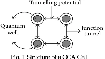
[image:2.612.224.392.540.635.2]The most fundamental element of the QCA structure is shown in figure 1. It is the building block of the QCA technology. As we can see in the figure it is having four dots at all its corner. The structure has two free electrons. The structure of the QCA in provided in the figure 1.
Fig. 1 Structure of a QCA Cell
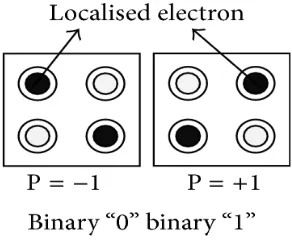
Fig. 2 Fig.2 QCA cell with two polarization
The diagonally opposite electrons interact to each other by the electrostatic forces and due to this force the electrons maintain its polarization. However the QCA cells cannot flow the data intrinsically therefore to get the control over flow of the direction of electrons the four clock zones are associated. These four clock signal have 90◦ phase difference. The QCA design is partitioned into clock zones. The clock scheme, named the zone clocking scheme, makes the QCA designs different polarizations intrinsically pipelined. Since each clock zone behaves like a D-latch [14]. The latter is provided by means of four clock signals clk x (with x ranging from 0 to 3), shifted by 90◦ from each other [1].
The fundamental logic gates available within the QCA technology are the inverter and the majority gate (MG). Given three inputs a, b, and c, the MG performs the logic function reported in equation (1) provided that all input cells are associated with the same clock signal clk x, whereas the remaining cells of the MG are associated with the clock signal clk x+1.
M (a, b, c) = a·b + a·c + b·c. (1)he 1-digit BCD adder earlier proposed in [16]–[17] use the top-level architecture in Fig. 3. In this the inputs are added in the binary format and then perform the conversion of BCD. If the output is greater than the 9 than 6 is added in it, else the addition of 0 is take place.
III. PROPOSED 32BITS BCD ADDERS IN QUANTUM-DOT CELLULAR AUTOMATA
In brief this proposes a unique approach to develop a QCA- based 32 bits BCD adder which can achieve higher computational speed than existing counterparts with occupying less area or count cell. The novel 1-digit decimal adder generates, propagates, and absorbs a carry signal with delay times up to 27%, 45%, and 44% lower than the faster existing counterparts that are those described in [8]. Differently from all previous works, we extended our work to the design of a 32-bits QCA-based BCD adder.
Fig 3.Structure of the 32 bits BCD adder.
The BCD adder here presented follows the traditional top-level structure illustrated in Fig. 3, but it exploits the novel logic expressions demonstrated in the following by Equations1 and 2.
[image:3.612.159.473.489.622.2]Fig. 4 New ADD1 module.
Ci+1 = M(dAi,dBi,Ci) ……. (2a)
Ci+2= M(Ci,M(dAi+1,dBi+1,gi),M(dAi+1,dBi+1,pi)) ……… (2b)
Consequently, the propagation of Ci through two bit positions would require two cascaded MGs to obtain the carryCi+2. Conversely, as discussed in [19] and given in (2b), by exploiting the auxiliary generate and propagate signals gi =dAi·dBi and pi =dAi·dBi, the carry Ci+2 can be computed by propagating Ci through just one MG. Equation 1 demonstrates a novel way to propagate Ci through two consecutive bit positions that also introduces just one MG between Ci and Ci+2 but avoiding the computation of gi and pi.
As a consequence of Equation 1, the 4-b adder ADD1 can be realized by computing the carries as reported in C1 = M(dA0,dB0,cin)
C2 = G1+P1·G0+P1·P0·
Cin = M(Cin, M(dA1,dB1,dA0),M(dA1,dB1,dB0))
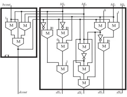
Fig. 5 Module CL and New ADD2module.
C3=M(dA2,dB2,C2C4=bcout=G3+P3·G2+P3·P2·C2 =M(C2,M(dA3,dB3,dA2),M(dA3,dB3,dB2)). (4)
[image:4.612.179.401.431.600.2]Fig. 2 shows the QCA circuit purpose-designed for the ADD1 module exploiting the aforementioned described logic. It is worth noting that, to compute C3, both (2a) and (3) could be used. The resulting circuits are depicted in the insets of Fig. 2. The former is actually exploited since propagating C1 instead of C2 would not reduce the overall delay of ADD1. Indeed, using (3) would lead to unnecessary additional MGs.
Due to Equation 1, the novel circuit exhibits a critical computational path of five MGs and one inverter, which is one MG shorter than the conventional Ripple-Carry Adder (RCA) [18]. Moreover, the novel ADD1 module uses only 16 MGs and 4 inverters, thus overcoming also the conventional 4-b CLA [19], which is implemented using 43 MGs and 4 inverters. The decimal carryout dcout and the decimal sum dS(3:0) are then calculated following the novel approach demonstrated in Equation 2.
Equation 2: If bcout and bS(3:0) are the binary carry-out and the binary sum computed by adding the BCD digits dA(3:0) and dB(3:0) then the BCD carry-out dcout is given by (6) and the decimal sum dS(3:0) is obtained by (7).
It is worth noting that the proposed circuit allows transforming the binary results coming from ADD1 to the BCD format through only four cascaded MGs, which are well below the eight and seven required by the ADD2 adders used with the same objective in [8],[15] and[16] respectively.
This whole process has been done using verilog HDL. For writing the code we use Xilinx ISE 13.2. The simulation of the program observed in the Model Sim. The above equations are written in the algorithm to realize the functionality of the developed circuit. We got the area in terms of LUTs. And performation in form of delay timing.
IV. RESULTS
After apply such innovative to the BCD adder we got the better result in terms of performance and number LUTs. The delay is reduced to dramatically reach the new level. As mentioned the LUTs have been reduced it means that the occupied area is less than the exiting adder.
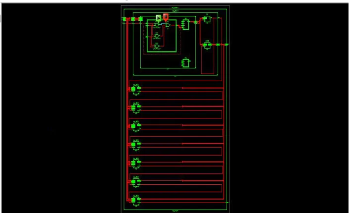
[image:5.612.127.480.501.716.2]The RTL view schematic of the circuit is shown in fig. 6.
Table .1 Device Utilization Summaries.
Logic Utilization Used Available Utilization
Number of Slice LUTs 72 192800 0%
Number of fully used LUT-FF pairs
0 72 0%
Number of bonded IOBs
98 600 16%
We observe from table 1 that LUTs used by design is 72 whereas the total available LUTs are 192800 which around zero percent so we can conclude that the developed system is very much reliable as well as efficient in term of area. Now we took number of fully used LUT-FF pairs we have found that the total available LUT-FF are 72 in counts but we didn’t use a single LUT-FF. The factor we have observed in the list is number of bonded IOBs in this section we used 98 IOBs whereas total available IOBs are 600. We have use 16% of IOBs of device. The number of LUTs is reduced as compare to any other digital adders. In short we can say that the developed device is efficient in term of area.
[image:6.612.93.519.289.490.2]One of the important factors in the observation is time delay. Now in the observation part of time we have delay of 16.478 ns. The individual component took the different time which varies between 0.279ns to 0.595ns.
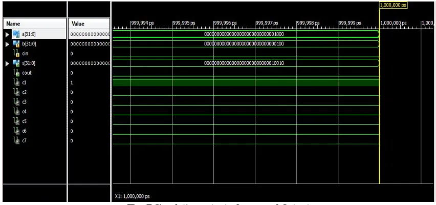
Fig. 7 Simulation output of proposed Output
Figure 9 shows the output of the developed BCD adder. The total number of inputs are three in which “a”and “b” are inputs whereas the third input is our carry in. Here the “a” and “b” both having 32 bit size. Carry in is represented as “cin”. “cin” is responsible to hold the value of 1 bit. It carries the value which was generated during the last operation. If there is no carry then put zero as its value. There are two outputs in the whole system. The first output is sum which is represented by the “s”. The size of the “s” is 32 bits. Another input is carryout. Carryout is denoted by “cout”. The “cout” having capacity to hold 1 bit value. In the following we have provided the input and output values.
Inputs
a[31:0]= 32`b00000000000000000000000000001000, b[31:0] = 32`b00000000000000000000000000000100, cin= 0,
Outputs
S[31:0]=32`b00000000000000000000000000010010, Cout=0.
V. CONCLUSION
implemented the QCA technology in the 32bits of BCD adder. The result of the 32bits of BCD adder based of QCA have already mentioned in the last section of the result.
At last after consideration of the factor we can conclude that implementation of the QCA technology provides the better result.
Table. 2 Comparison Results of 16 bits BCD Adder.
Adder Cells Area[nm2] Clock Cycles
[16] 1348 2.28 8
[20] 1130 1.77 10
[21] CFA-based 932 1.36 4.75
[21]CLA-based 1838 1.86 2.5
[22] 1065 1.36 3.5
REFERENCES
[1] C. S. Lent, P. D. Tougaw, W. Porod, and G. H. Bernestein, “Quantum cellular automata, ”Nanotechnology, vol. 4, no. 1, pp. 49–57, 1993 [2] M. T. Niemer and P. M. Kogge, “Problems in designing with QCAs: Lay-out=timing,”Int. J. Circuit Theory Appl., vol. 29, pp. 49–62, 2001.
[3] K. Navi, M. H. Moaiyeri, R. F. Mirzaee, O. Hashemipour, and B. M. Nezhad, “Two new low-power full adders based on majority-not gates,”Microelectron. J., vol. 40, pp. 126–130, 2009.
[4] H. Cho and E. E. Swartzlander Jr., “Adder design and analyses for quantum-dot cellular automata,”IEEE Trans. Nanotechnol., vol. 6, no. 3,pp. 374–383, May 2007
[5] H. Cho and E. E. Swartzlander Jr., “Serial parallel multiplier design in quantum-dot cellular automata,” inProc. IEEE Symp. Comput. Arithmetic, 2007, pp. 7– 15
[6] S. W. Kim and E. E. Swartzlander Jr., “Parallel multipliers for quantum-dot cellular automata,” inProc. IEEE Nanotechnol. Mater. Devices Conf., 2009, pp. 68– 72
[7] S. W. Kim and E. E. Swartzlander Jr., “Multipliers with coplanar crossings for quantum-dot cellular automata,” inProc. IEEE Int. Conf. Nanotech-nol., 2010, pp. 953–957
[8] W. Liu, L. Lu, M. O’Neill, and E. E. Swartzlander Jr., “Montgomery modular multiplier design in quantum-dot cellular automata using cut-set retiming,” inProc. IEEE Int. Conf. Nanotechnol., 2010, pp. 205–210
[9] L. Lu, W. Liu, M. O’Neill, and E. E. Swartzlander Jr., “QCA systolic matrix multiplier,” inProc. IEEE Annu. Symp. VLSI, 2010, pp. 149–154
[10] J. D. Wood and D. Tougaw, “Matrix multiplication using quantum-dot cellular automata to implement conventional microelectronics,”IEEE Trans. Nanotechnol., vol. 10, no. 5, pp. 1036–1042, Sep. 2011
[11] B. Sinharoy et al., “IBM POWER8 processor core microarchitecture,” IBM J. Res. Dev., vol. 59, no. 1, pp. 1–21, Jan./Feb. 2015 [12] L. Eisen et al., “IBM POWER6 accelerators: VMX and DFU,” IBM J.Res. Dev., vol. 51, no. 6, pp. 1–21, Nov. 2007
[13] IEEE Standard for Floating-Point Arithmetic, IEEE Working Group of the Microprocesser Standards Subcommittee, IEEE Std. 754-1985, 2008.
[14] J. D. Wood and D. Tougaw, “Matrix multiplication using quantum-dot cellular automata to implement conventional microelectronics,”IEEE Trans. Nanotechnol., vol. 10, no. 5, pp. 1036–1042, Sep. 2011
[15] M. Taghizadeh, M. Askari, and K. Fardad, “B.C.D. computing structures in quantum-dot cellular automata,” in Proc. IEEE, Conference. Computer. Communication. Engg., Kuala Lampur, Malaysia, pp. 1042–1045, May 2008
[16] F. Kharbash and G. M. Chaudhry, “The design of quantum-dot cellular automata decimal adder,” inProc. IEEE Int. Multitopic Conf., Karachi, Pakistan, pp. 71– 75, , Dec. 2008
[17] V. Pudi and K. Sridharan, “Efficient design of a hybrid adder in quantum-dot cellular automata,”IEEE Trans. Very Large Scale Integr. System, vol. 19, no. 9, pp. 1535–1548, Sep. 2011
[18] V. Pudi and K. Sridharan, “Low complexity design of ripple carry and Brent-Kung adders in QCA,”IEEE Trans. Nanotechnol., vol. 11, no. 1,pp. 105–119, Jan. 2012
[19] H. Cho and E. E. Swartzlander, Jr., “Adder design and analyses for quantum-dot cellular automata,”IEEE Trans. Nanotechnol., vol. 6, no. 3, pp. 374–383, May 2007.
[20] M. Gladshtein, “Quantum-dot cellular automata serial decimal adder,” IEEE Trans. Nanotechnol., vol. 10, no. 6, pp. 1377–1382, Jun. 201
[21] W. Liu, L. Lu, M. O’Neill, and E. E. Swartzlander, “Cost-efficient decimal adder design in quantum-dot cellular automata,” inProc. IEEE Int. Symp. Circuits Syst., Seoul, South Korea, May 2012, pp. 1347–1350