Understanding the
p
-type defect chemistry of CuCrO
2
David O. Scanlon
*
and Graeme W. Watson
*
Received 9th November 2010, Accepted 6th January 2011 DOI: 10.1039/c0jm03852k
CuCrO2is the most promising Cu-based delafossite forp-type optoelectronic devices. Despite this, little is known about thep-type conduction mechanism of this material, with both CuI/CuIIand CrIII/CrIV hole mechanisms being proposed. In this article we examine the electronic structure, thermodynamic stability and thep-type defect chemistry of this ternary compound using density functional theory with three different approaches to the exchange and correlation; the generalized-gradient-approximation of Perdew, Burke and Ernzerhof (PBE), PBE with an additional correction for on-site Coulombic interactions (PBE +U) and the nonlocal, screened-exchange hybrid functional HSE06. The fundamental band gap of CuCrO2is demonstrated to be indirect in nature. Under all growth conditions, the dominant intrinsicp-type defect will be the Cu vacancy, with hole formation centered solely on the Cu sublattice. Mg doping is found to be significantly lower in energy than intrinsic defect formation, explaining the large increases in conductivity seen experimentally. Cu-rich/Cr-poor growth conditions are found to be optimal for both intrinsic and extrinsic (Mg doping) defect formation, and should be adopted to maximize performance.
I.
Introduction
Fabrication of high figure-of-meritp-type transparent conduct-ing oxides (TCOs) is a much sought after goal for optoelectronic devices.1 Realisation of a p-type TCO to rival the current
industry standard n -type TCOs (e.g. In2O3:Sn,2 ZnO:Al,3 SnO2:F4), would open up the possibility of ‘‘transparent elec-tronics’’.5An explosion of interest in CuIwide band gap mate-rials was spearheaded by Hosono and co-workers with their 1997 report of simultaneous p-type conductivity and optical trans-parency in thin films of delafossite CuAlO2.6Subsequently, many other p-type TCOs with the delafossite structure, including CuInO2,7 CuScO2,8 CuGaO2,9 CuYO210 and most recently CuBO2.11,12 have been investigated, but to date the delafossite with the highest reported conductivity (220 S cm1) is Mg-doped CuCrO213
In the delafossite structure each Cu atom is linearly coordi-nated with two oxygen atoms, forming O–Cu–O dumbbells parallel to the caxis. Oxygens in these O–Cu–O units are also each coordinated to three MIIIatoms, oriented such that MIII -centered octahedra form MIIIO
2layers which lie parallel to theab plane. Two alternative layer stackings are possible, resulting in a hexagonal (space group P63/mmc) or rhombohedral (space group R3-mh) unit cell,14 with CuCrO
2found to crystalize in both polymorphs.15,16
It is well known that doping the trivalent metal site in the delafossite structure with a divalent dopant significantly improves the conductivity,17but the conductivity trends seen for
different trivalent metal cations have remained contentious.
Nagarajan et al. attempted to explain the trend in
increasing conductivity of CuY1-xCaxO2 to CuSc1-xMgxO2 to CuCr1-xMgxO2by noting that the increasing conductivity tracks a decreasing ionic radius of the MIII cation, and hence a decreasing lattice paramater in the Cu ion plane.13They suggest
that this leads to increased Cu d orbital overlap and as a result better hole mobility. This size dependence theory can effectively be ruled out by the observed conductivity of CuAl1-xMgxO2, which at 4104S cm1has a much lower conductivity than that of CuCr1xMgxO2(220 S cm1), despite the ionic radius of Al being smaller than Cr.18
Sleight and co-workers have discussed the effect of the MIIIion on the mobility of holes in p-type delafossites.10 The authors
suggest that the lower hole mobilities in p-type delafossites relative to Cu2O may be caused by the lack of Cu–O–Cu linkages as seen in Cu2O. In the delafossite structure there are only Cu–O– MIII–O–Cu linkages. The authors suggest that the higher conductivities observed for CuCrO2and CuFeO2may be due to favourable mixing with the3d states on the MIII cation in the Cu–O–MIII–O–Cu linkages.10In a recent theoretical
investiga-tion of CuMIIIO
2(MIII¼Al, Cr, Y, Sc) it has been proposed that the Cr 3dstates appear in the valence band and mix with the O 2p, and that this increased covalency in the system leads to increased hole mobility.19
Very recently, CuCrO2has attracted attention for a range of applications other than TCO applications. In the condensed matter physics community, CuCrO2has been investigated for its unusual magnetic properties, due to its frustrated antiferro-magnetic ordering and multiferroic properties.20–30It has
gener-ated interest due to its catalytic abilities in hydrogenation
School of Chemistry and CRANN, Trinity College Dublin, Dublin 2, Ireland. E-mail: [email protected]; [email protected]
ª
Dynamic Article Links
C
<
Journal of
Materials Chemistry
Cite this:
J. Mater. Chem.
, 2011,
21
, 3655
www.rsc.org/materials
PAPER
Downloaded by Trinity College Dublin on 02 April 2012
reactions,31 its ozone sensing properties,32,33 and as a possible
thermoelectric material.34,35CuCrO
2has also been identified as a possible photocatalyst for hydrogen evolution,36 NO
237and
NO
338removal, and removal of M2+(M¼Ni, Cu, Zn, Cd, Hg).39 The nature of the band gap of CuCrO2has been a source of controversy in the literature, with some experimental studies reporting an indirect band gap,40–42and others finding CuCrO
2to be a direct band gap semiconductor.43 The earliest recorded
measurement of the band gap of CuCrO2 was carried out by Benko and Koffyberg,40who found that it possessed an indirect
band gap of 1.28 eV, with an indirectallowedtransition at 3.08 eV and a direct allowed transition at 3.35 eV. A further interband transition at2.20 eV was noted, although the authors were not able to determine the transition type.40In general, recent optical
measurements have found thedirectoptical band gap to be in the range 2.95–3.30 eV, meaning CuCrO2is transparent to visible light.13,44–49
Rastogiet al.have recently reported for 155nm (305 nm) thick, spray deposited thin films for Mg-doped CuCrO2, indirect band gaps of 2.58 eV (2.79 eV) and direct band gap of 3.08 eV (3.14 eV).41 Mahapattra and Shivashanhar have also reported
thin films of CuCrO2formed using chemical vapour deposition to possess an indirect band gap of 2.63 eV and a direct band gap of 3.08 eV.42Conversely, Liet al.have reported that no indirect
band gap exists in their CuCrO2thin films prepared by pulsed laser deposition, with thefundamentalband gap being direct and measuring 3.20 eV.43
Undoped CuCrO2is a semi-conductor with a high resistivity, however, substitution of divalent dopants (e.g.Mg, Ca, Ni) for trivalent Cr in this system leads to a marked increase in conductivity.13,20,21,29,35,45,50This increase in conductivity has been
linked to CuI/CuII,51,52and to CrIII/CrIVhole mechanisms.34All
other delafossites are thought to conduct via the CuI/CuII mechanism,40,53–58 and recent high resolution X-ray
photoelec-tron spectroscopy (XPS) studies in conjunction with GGA +U
calculations have shown that Cu states dominate at the VBM, indicating the likelihood of a copper hole mechanisms.59GGA
calculations have, however, indicated that Cr states dominate at the VBM, and in conjuction with magnetoresistance studies, this was reported to indicate a CrIII/CrIVmechanism.60
In this study we address two main questions about the funda-mental chemistry/physics of CuCrO2: (a) what is the nature of the band gap of CuCrO2? (b) What is the conductivity mechanism of CuCrO2, do holes exist on the Cu or the Cr states? Using PBE, PBE +Uand the screened hybrid functional HSE06, we investigated the band structure of CuCrO2, and investigate threep-type defects in CuCrO2, namely copper vacancies (VCu), oxygen interstitials (Oi),
and Mg dopants on a Cr lattice site (MgCr). We show: (i) PBE +U and HSE06 predict that the states that dominate at the VBM are Cu 3dstates, consistent with previous XPS experiments,59with GGA
providing a very poor description of the location of both the Cu and Cr 3dlevels, (ii) with all three approaches, CuCrO2is found to possess an indirect band gap, (iii) VCuis the dominantintrinsic
p-type defect in CuCrO2, (iv) MgCrdefect formation energies are lower than intrinsicp-type defect energies under all growth condi-tions, and (v) acceptor defects in CuCrO2form holes on the Cu
dstates, and not on the Crdstates as had previously been proposed. In light of these results we discuss the increased conductivity of CuCrO2relative to other delafossite TCOs.
II.
Theoretical methods
All calculations were performed using the VASP code,61with the
projector augmented wave (PAW) approach.62The calculations
were performed using the Genaralized Gradient Approach (GGA) of Perdew, Burke, and Ernzerhof (PBE),63PBE corrected
for on-site Coulomb interactions (PBE +U), and the screened hybrid functional as proposed by Heyd, Scuseria, and Ernzerhof (HSE06).64 HSE06 consistently produces structural data and
band gap descriptions that are more accurate than LDA/GGA andmeta-GGA data.12,65–74 For the PBE +U calculations, we
apply the rotationally invariant approach of Dudarev.75 We
utilizedUCudof 5.2 eV which closely reproduces features of the experimental X-ray photoemission spectroscopy (XPS) spectra for Cu2O and has been shown to reproduce the valence band features of many delafossites.59,76,77ThisUis also similar to theU
values used by Raebigeret al.of 5 eV (which was also chosen to reproduce features of a Cu2O XPS valence band spectra78), and the value of 6 eV chosen by Huda et al. to account for the correlation in narrow 3d-bands.79AUvalue of 4 eV was chosen
for the Cr d states, which has been shown to reproduce the valence band features of Cr2O3.80Interactions between the cores (Cu:[Ar], Cr:[Ar] and O:[He]) and the valence electrons were described using the PAW method.81While the exotic magnetic
interactions in CuCrO2 are of much interest,20–30 reproducing these interactions is not feasible with the large supercells and computationally expensive methods used in this study. There-fore, we employed a simplified antiferromagentic (AF) ordering for our calculations, consisting of planes of ferromagnetically ordered Cr states, with AF layer–layer interactions (taken from PBE +Utest calculations). We considered only the hexagonal (Space groupP63mmc, #194) polymorph of CuCrO2to allow us to simulate the known AF ordering within the unit cell.
In each method utilized, the atomic positions, lattice vectors and cell angles were allowed to relax, while the total volume was held constant. The resulting energy volume curves were fitted to the Murnaghan equation of state to obtain the equilibrium bulk cell volume.82This approach avoids the problems of Pulay stress
and changes in basis set which can accompany volume changes in plane wave calculations. Convergence with respect to k-point sampling and plane wave energy cut off was checked, with a plane wave cutoff of 400 eV andk-point sampling of 441 found to be sufficient for each method (tests were conducted at 500 eV andk-point sampling of 553 for all three methods, which showed a convergence of 0.005 eV/f.u.). For the density of states plots, however, we have used ak-point sampling of 99
5. The structure was deemed to be converged when the forces on all the atoms were less than 0.01 eVA1. As CuCrO
2contains open-d shells Cr atoms, all calculations were spin polarized. Defects were calculated in a 441 (128 atom) supercell, and structure visualization and analysis were performed using VESTA.83
The formation enthalpy of a defect with charge stateqis given by
DHfðD;qÞ ¼
ED;qEH
þX
i
niðEiþmiÞ þq
EFermiþeHVBM
þEalign½q: (1)
ª
Downloaded by Trinity College Dublin on 02 April 2012
EHis the total energy of the stoichiometric host supercell andED,q
is the total energy of the defective cell. Elemental reference energies,Ei, were obtained from calculations on the constituent
elements in their standard states,i.e.Cu(s)Cr(s)and O2(g),miis the
chemical potential of the constituent element, and n is the number of atoms formally added to or taken away from an external reservoir.EFermiranges from the VBM (EFermi¼0 eV) to the CBM. 3H
VBM is the VBM eigenvalue of the host bulk.
Ealign[q] is the correction that (i) accounts for the proper align-ment of the VBM between the bulk and the defective supercells and (ii) corrections for the finite-size-cell effects in the calcula-tions of charged impurities, as outlined by Freysoldtet al.84The
thermodynamic transitions (ionization) levels (TLs) of a given defect, 3D(q/q
0
), are equal to the Fermi-level for which charge statesqandq0
have equal energy:
eD
q=q0¼DH
fðD;qÞ DHfD;q0
q0q (2)
III.
Results
A. Equilibrium structures
The PBE, PBE + U and HSE06 calculated structures for
hexagonal CuCrO2are shown in Table 1. The PBE calculated lattice parameters are overestimated compared to experiment, but this is a known overestimation of the GGA method.85PBE + Uoverestimates thealattice parameter by more than the PBE, but has an improved c parameter. Minimization with HSE06 yields acparameter that is in excellent agreement with experi-ment,15but with an overestimatedaparameter. Overall, HSE06
yields the closest lattice parameters to experiment, which is not surprising, as the HSE06 functional regularly yields structural information that is more accurate than standard DFT methods. HSE06 consistently produces structural data and band gap descriptions that are more accurate than LDA/GGA andmeta -GGA data.12,65–74
B. Electronic structure
The PBE, PBE +Uand HSE06 calculated band structures for hexagonal CuCrO2are shown in Fig. 1. For all three methods, the VBM is located on the K toGline, near K, with the CBM found on the M-Gline, indicating that CuCrO2 is anindirect band gap material, and not a direct band gap materials as had been suggested previously.43 The calculated indirect band gaps
are 1.06 eV, 2.06 eV and 3.09 eV using PBE, PBE +Uand HSE06 respectively. The PBE calculated band structure features are visibly different to those of the PBE + U and HSE06 band structure, possessing a much less dispersive valence band.
Upon analysis of the PBE, PBE + Uand HSE06 calculated total and partial (ion decomposed) electronic densities of states (EDOS/PEDOS) for CuCrO2, Fig. 2, the reason for the flatter band structure features for the PBE band structure become apparent. In the PBE EDOS/PEDOS, the Cr 3dstates dominate at the VBM and the CBM, whereas in the PBE +Uand HSE06 EDOS/PEDOS, the Cr 3d states are pushed to lower energies relative to the VBM, with Cu 3dstates dominating at the VBM in both cases, making the valence band visibly more disperse in the band structures, Fig. 1. The Cu 3dpeak positions for both the PBE +Uand the HSE06 PEDOS are situated at2.1 eV, with the Cu 3dpeaks centered at1.75 eV using PBE. High reso-lution XPS studies have placed the Cu 3dpeak at2.1 eV,59
indicating that the HSE06 and PBE +Utreatment of the known self interaction error of the Cu 3dstates is probably satisfactory, but is not satisfied at all in the case of PBE. The Crd-dsplitting is appreciably increased in the PBE +Uand HSE06 calculations compared to the PBE.
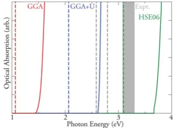
C. Optical analysis
The optical absorption spectra for CuCrO2, calculated using PBE, PBE +Uand HSE06, are shown in Fig. 3. With PBE, and using the Tauc relation (Egfa2), the onset of optical absorption
[image:3.595.43.288.94.168.2]begins at 1.5 eV, which is considerably underestimated
Table 1 Structural data and nearest-neighbour interatomic distances for the optimized PBE, PBE + U and HSE06 optimized CuCrO2structures,
compared to experimental data.86Volumes are given inA3and lattice
dimensions and interatomic distances inA
PBE PBE + U HSE06 Expt.15
a 3.01 3.05 3.01 2.97
c 11.47 11.42 11.40 11.40
Volume 90.04 92.25 89.73 87.32
dCr–O 2.01 2.03 2.01 1.99
dCu–O 1.86 1.84 1.86 1.85
Fig. 1 (a) PBE, (b) PBE + U and (c) HSE06 calculated band structures for CuCrO2.
ª
Downloaded by Trinity College Dublin on 02 April 2012
[image:3.595.89.504.569.719.2]compared to the experimental range of 2.95–3.30 eV.13,44–49
PBE +Uprovides an improved description of the optical band gap compared to experiments, with a calculated optical band gap of2.7 eV, however, thisdirectband gap is only in the range of the indirect band gaps reported in experiment. The HSE06 optical band gap is calculated to be 3.75 eV, which is an overestimation of 0.45 eV over the largest experimentally reported optical band gaps for CuCrO2. In line with these find-ings, HSE06 has been shown recently to overestimate the band gaps of some transition metal containing ternary oxide systems.87
Fitting exchange to the band gap is an often-used correction when the hybrid function of choice does not yield the expected band gap,70,88 however, in this case there are too many
uncer-tainties about the exact indirect and direct band gaps of CuCrO2, so we have not attempted any ‘‘exchange fitting’’ in this case. The earliest study of the opto-electronic properties of CuCrO2 by Benko and Koffyberg40had reported an indirect band gap of
only 1.28 eV. The same authors also studied CuAlO2,57 and
consistent with many other studies89reported an indirect band
gap of 1.65 eV for CuAlO2. Recent experiments89,90and calcu-lations91,92have called into question the validity of these ‘‘indirect
band gap’’ signals in CuAlO2, and postulate that they stem from defect absorptions, as the absorptions commonly attributed to these Eind
g possess optical absorption coefficients that are in excess
of two orders of magnitude larger than typical indirect absorp-tion edges.89A thorough re-investigation of the exact nature of
the band gap of CuCrO2is thus warranted.
D. Thermodynamic stability of CuCrO2
By varying the chemical potentials,mi, we can simulate the effect of varying the partial pressures experimentally, setting the conditions under which CuCrO2 forms. In this way, we can determine the optimum conditions forp-type defect formation, within the constraint of the calculated enthalpy of the host:mCu+
mCr+2mO¼DHCuCrO2f. To avoid precipitation into solid elemental Cu, Cr and O2gas we also require:mCu#0,mCr#0,mO#0. The chemical potentials are further constrained by the decomposition of CuCrO2into binary compounds:mCu+mO#DHCuO2f,mCu+
mO#DHCu2Of and 2mCr+ 3mO# DHCr2O3f. A boundary is also imposed when Mg doping, as we try to avoid the formation of MgO: mMg + mO # DHMgOf . The PBE, PBE + U and HSE06 calculated formation energies of the oxides considered are given in Table 2.
Following the approach of Walshet al.94and Perssonet al.,95
the phase diagram for CuCrO2 can be drawn up as in Fig. 4 which shows the range of chemical potentials under which CuCrO2 forms, calculated using HSE06. The triangle vertices correspond to Cr/O-rich conditions (mCr ¼ mO¼ 0.00, mCu¼
6.85), Cu/O-rich conditions (mCr ¼ 6.85, mCu¼mO¼0.00) and Cu/Cr-rich conditions (mCr¼mCu¼0.00mO¼ 3.43) and are calculated directly frommCu+mCr+ 2mO¼DHCuCrO2f¼ 6.85 eV. The boundaries for binary phase formation are then calcu-lated from the binary equations. This results in a narrow range of chemical potentials under which CuCrO2is thermodynamically stable. Within these boundaries we explicitly consider four conditions, as marked in Fig. 4. Environment A in Fig. 4, corresponds to Cr-poor, Cu-poor and O-rich conditions. Envi-ronment B is at the Cr-poor limit, withmCuandmOhaving mid-range values, with condition C corresponding to the Cu-rich limit of the stability region, with a mid rangemCrand a relatively low
mO. Lastly, environment D represents Cr-rich, O-poor and Cu-rich limits, which should favour the formation of oxygen poor (or n-type) defects. This analysis was repeated using PBE and PBE +U, with the corresponding chemical potential limits for each method in each environment shown in Table 3.
Fig. 2 Electronic density of states for CuCrO2calculated using (a) PBE,
(b) PBE + U and (c) HSE06. The total DOS, Cud, Crdand O 2pstates are colored black blue, green and red, respectively.
Fig. 3 Calculated optical absorption spectra of CuCrO2summed over
[image:4.595.74.260.50.260.2]all possible direct valence to conduction band transitions. PBE (red) PBEU(blue), HSE06 (green) and Experiment (grey). Dashed lines indi-cate indirect band gaps, solid lines indiindi-cate optical absorptions.
Table 2 Formation enthalpies of CuCrO2 and the relevant binaries
calculated using PBE, PBE + U and HSE06 and comparison with experiment
Structure PBE PBE + U HSE06 Expt.93
Cu2O 1.23 1.55 1.55 1.73
CuO 1.18 1.36 1.40 1.61 Cr2O3 9.99 10.64 11.64 11.69
MgO 3.97 5.51 5.74 6.24 CuCrO2 5.70 6.33 6.85 —
ª
Downloaded by Trinity College Dublin on 02 April 2012
[image:4.595.78.252.320.448.2] [image:4.595.308.555.652.726.2]E. Defect energetics and transition levels
Table 4 lists the neutral formation energies of the differentp-type defects under the four differing growth conditions as outlined
above for PBE, PBE + U and HSE06. It is clear that the
formation energies are lowest for environment A (Cu-poor/Cr-poor/O-rich), and as such these conditions should be enforced to maximise p-type performance of undoped and acceptor doped CuCrO2samples.
Fig. 5 displays a plot of the formation energy ofp-type defects in CuCrO2(copper vacancies VCu, oxygen interstitials Oi, and
Mg-dopants MgCr) under Cu-poor/Cr-poorconditions as a func-tion of Fermi-level posifunc-tion, calculated using PBE, PBE +Uand HSE06. At first glance, there are some very evident trends in formation energies. The formation energy of all three defects considered increases as the complexity of the theoretical method utilized is increased,i.e.PBE < PBE +U< HSE06. A similar trend was also noted previously in studies of p-type defects in Cu2O.70,96
Secondly, for each method the formation energy of MgCr is lower than the formation energy of VCu. GGA predicts the formation energy of MgCrto be spontaneouswith a formation energy of0.53 eV, and predicts the formation energy ofVCuto be only 0.16 eV. PBE +Upredicts that the formation energy of MgCrcostsenergy (0.46 eV), with HSE06 predicting the forma-tion energy to be 0.62 eV. The results of thehighercomplexity calculations are very different, and highlight the need for caution when interpreting defect formation energies calculated using standard DFT functionals, such as GGA or LDA. The GGA results can serve only as an indicator of the energetic trends in
Fig. 4 Illustration of the accessible (mCu,mCrchemical potential range
[image:5.595.63.266.49.205.2]for CuCrO2calculated using HSE06.
Table 3 The PBE, PBE + U and HSE06 calculated chemical potentials at the four chemical potential limits imposed by the formation of competing binary oxides for CuCrO2, as indicated in Fig. 4. All energies are given in eV
PBE PBE +U HSE06
mCr mCu mO mCr mCu mO mCr mCu mO
A 3.65 0.34 0.86 4.24 0.65 0.71 4.72 0.67 0.73 B 3.39 0.06 1.23 3.79 0.19 1.17 4.20 0.15 1.25
C 3.24 0.00 1.23 3.22 0.00 1.55 3.75 0.00 1.55
[image:5.595.336.515.50.246.2]D 2.66 0.00 1.52 2.29 0.00 2.02 2.72 0.00 2.07
Table 4 The PBE, PBE + U and HSE06 calculated neutral defect formation energies forVCu, Oiand MgCrat the four chemical potential limits imposed
by the formation of competing binary oxides for CuCrO2, as indicated in Fig. 4. All energies are given in eV
PBE PBE +U HSE06
VCu Oi MgCr VCu Oi MgCr VCu Oi MgCr
A 0.16 1.27 0.54 0.95 1.38 0.46 1.45 1.63 0.62
B 0.45 1.54 0.54 1.41 1.85 0.46 1.97 2.15 0.62
C 0.50 1.65 0.50 1.60 2.23 0.65 2.12 2.45 0.77
D 0.50 1.94 0.21 1.60 2.69 1.11 2.12 2.96 1.29
Fig. 5 PBE (red), PBE + U (blue) and HSE06 (red) calculated formation energies forp-type defects in CuCrO2as a function of Fermi energy under
Cu-poor/Cr-poor conditions. The solid lines denote MgCr, the dashed
lines denoteVCu, and the dot-dot-dahs lines denote Oifor each method. The vertical dotted lines denote the calculated CBM for each method, and the solid dots denote the transition levels3(q/q0
).
ª
Downloaded by Trinity College Dublin on 02 April 2012
[image:5.595.43.550.514.596.2] [image:5.595.44.553.645.726.2]formation energy, but cannot reveal any quantitative informa-tion about formainforma-tion energies.
The HSE06 formation energy ofVCu(1.45 eV) is close to that of the HSE06 calculated formation energy for VCuin CuAlO2 (1.33 eV).92The HSE06 calculated formation energy for an O
iin
CuCrO2is 1.63 eV, however, which is considerably lower than the HSE06 calculated formation energy of an Oiin CuAlO2(3.10 eV).92 This difference can be explained by the larger lattice
parameters of CuCrO2, which means there is more space for Oito
form.
For all three methods employed, activated conductivity is predicted, although it should be noted that, without the explicit inclusion of a correction for finite size effects and valence band alignment,84 the PBE transition levels for V
Cu and MgCr are actually resonant in the valence band. Previous standard DFT studies of the defect chemistry/physics of delafossites have neglected to deal with finite size effects and valence band align-ments, and as such the incorrect prediction of degenerate conductivity for CuAlO2for example,97,98is not surprising.
The transition levels for all three defects get deeper as you move from PBE to PBE +Uto HSE06. The (0/1) transition level for theVCuwith HSE06 is 0.37 eV, which is considerably shallower than the HSE06 calculated transition levels for CuAlO2at 0.68 eV.92The experimentally reported acceptor level for CuAlO2is 0.70 eV,90which is a good indicator of the reli-ability of the HSE06 transition levels for delafossite systems.
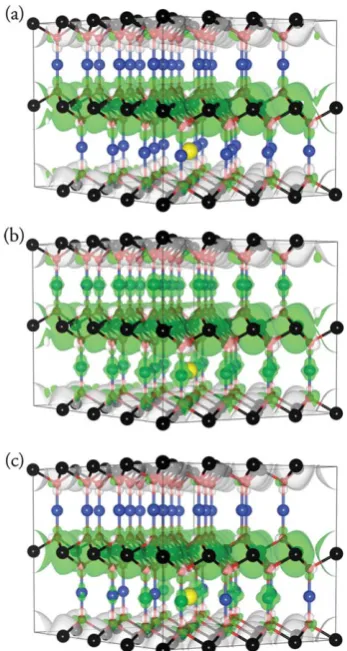
F. Hole localization/delocalization
[image:6.595.342.516.52.378.2]To elucidate the mechanism of hole formation in CuCrO2, we have plotted the spin density (difference between the alpha and beta spin) for theVCuin CuCrO2, with the results displayed in Fig. 6. Upon examination of the spin density for the PBEVCu, it becomes apparent that no hole density is present on the Cu atoms, with all the hole density mixed in with the Cr spins. This is not surprising, as the Cr states dominate at the VBM in the PBE description, and as such holes would be expected to form on Cr states. This situation changes when we move to PBE +U, with the hole density now delocalized over all the Cu atoms in the cell, with no change in the Cr spin density. For the VCucalculated using HSE06, the hole density is only localized/delocalized on the Cu states surrounding the vacancy, but not in the neighbouring Cu layers. It is therefore apparent that the higher levels of theory predict that hole formation will be centered on the Cu atoms, and that a CrIII/CrIVhole mechanism is unlikely. HSE06 predicts the holes on the Cu sites to be less localized than holes formed from aVCuin CuAlO2.92
IV.
Discussion
Delafossites and CuI oxides in general are considered to be polaronic,53–56,58,70,96,99–106and as such it is expected that the Cu–
Cu distances should play a part in any conductivity, with holes expected to hop from Cu to Cu.58The Cu–Cu distance (equal to
thea/blattice constant) is determined by the size of the MIIIion, which suggests that the conductivity will increase as the size of the MIIIion decreases. In fact this seems to be true for CuBO
2, which has the smallest Cu–Cu distance of all delafossites, and is reported to have the highest non-doped conductivity.11 This
would also explain why undoped CuAlO2has been reported to have a higher conductivity than both undoped CuScO2 and CuYO2.18
However, conduction in these systems cannot be as simple as stating that conductivity is inversely proportional to MIIIradii size. The number of hole carriers (introduced by intrinsic or extrinsic defects) in the system is also very important, with size of the MIIIagain thought to play an important role. The size of the MIIImay determine the non-doped conductivity of these mate-rials, as the larger the MIIIion, the more oxygen interstitials the material can contain.10,107This is consistent with the the reported
undoped conductivity of CuYO210being higher a higher than CuScO2.108It cannot, however, explain why CuCrO2has a higher undoped conductivity even than CuAlO2.18
As the size of the trivalent ion increases, It is postulated that the ability to dope the material also increases.109By this
ratio-nale, extrinsic doping of CuAlO2to increase carrier concentra-tions and lower the Fermi level could be substantially more difficult than doping CuYO2for instance. This does not take into account, however, that suitably sized dopants for most trivalent cations can be found. It is known that there is a very limited range for MgIIsubstitution in CuCrO
2, withx¼0.05 being the limit for CuCr1-xMgxO260 Despite this, the conductivity of
CuCrO2:Mg is much higher than that of CuScO2:Mg and
Fig. 6 Spin density (alpha spin (green) - beta spin (white)) plot for CuCrO2calculated using (a) PBE, (b) PBE + U and (c) CuCrO2. Blue,
Black and red spheres denote Cu, Cr and O atoms respectively. The green/white isosurface is shown at 0.05eA3.
ª
Downloaded by Trinity College Dublin on 02 April 2012
CuYO2Ca, which should be able to contain a much higher dopant concentration. Therefore, the electronic structure of the MIIIion must also play a prominent role in conductivity.
Upon analysis of our calculated density of states, it is clear that the higher levels of theory (PBE +Uand HSE06) predict that the VBM of CuCrO2is dominated by Cu 3dstates, with our subse-quent analysis of the hole localization showing that holes are formed on the Cu atoms with these methods. HSE06 predicts that the holes are quite localized on the Cu atoms neighbouring a copper vacancy, but are not as localized as they are in CuAlO2.92 This ‘‘delocalization’’ of the hole state in CuCrO2 compared to CuAlO2is most likely due to the increased cova-lency of the CuCrO2system, with the Cr 3dstates mixing with the O 2pstates along the entire width of the valence band. This theory is also supported by our recent examination of the bader charges of CuMIIIO
2(MIII¼Al, Cr, Sc, Y)19which revealed that the trend of MIIIion covalency with oxygen follows Cr > Sc > Y > Al, with Cr having the largest covalent interaction. This trend follows exactly the experimentally known conductivity trend for the doped delafossite. This is not unexpected, as elementary chemical intuition tells us that a more delocalized, covalent valence band should improve hole mobility.
It is clear from these results that conductivity in delafossites is a synergy between both size and electronic structure of the MIII ions. The necessary requirements for good conductivity would appear to be (a) the MIIIion not being overly large, and thus not limiting the hole hopping, leading to good non-doped conduc-tivity; (b) the MIIIion having a favourable electronic structure, which can enhance the mobility of holes (delocalize holes states) and (c) the MIIIion not being too small and limiting the dop-ability of the material and hence allowing a high charge carrier concentration. Finding a compromise between these three factors is the key, and might plausibly explain why CuCrO2is currently the leading material, possessing a favourable electronic structure, and a MIIIion big enough to allow doping and small enough not to limit hopping.
V.
Conclusion
We have investigated the electronic structure and p-type defect chemistry of CuCrO2using PBE, PBE +Uand HSE06. We find that the fundamental band gap of CuCrO2is indirect with all
three methods, with PBE and PBE + U underestimating and
HSE06 overestimating the experimentally observed range of optical band gaps. PBE suggests that Crdstates will dominate at the VBM, with PBE +Uand HSE06 indicating that Cudstates will dominate at the top of the valence band, consistent with the majority of other copper-based delafossites and recent high resolution XPS studies. Mg doping on the Cr site is found to be more energetically favourable than intrinsic p-type defect formation, with all of the p-type defects considered yielding ionization levels deep in the band gap. Cu-poor/Cr-poor/O-rich conditions are found to be optimal for both intrinsic p-type defect formationandacceptor doping, and these growth condi-tions should be adopted to maximize performance. Both of the higher levels of theory (PBE + U and HSE06) predict that CuCrO2conducts through a CuI/CuIIhole mechanism, and not
viaa CrIII/CrIVhole mechanism as has been previously suggested.
The higher conductivities of CuCrO2 compared to other
delafossites is attributed to favourable mixing of Crdstates with O 2pstates in the valence band, producing shallower transition levels for the Cu-based holes.
Acknowledgements
This publication has emanated from research conducted with financial support of Science Foundation Ireland: PI Grant Number 06/IN.1/192 and 06/IN.1/192/EC07. We also acknowl-edge support from the HEA for the PTRLI programs IITAC (Cycle III) and e-INIS (CYCLE IV). All calculations were per-formed on the IITAC supercomputer as maintained by the Trinity Centre for High Performance Computing (TCHPC) and the Stokes computer, maintained by the Irish Centre for High-End Computing (ICHEC).
References
1 K. Hayashi, S. Matsuishi, T. Kamiya, M. Hirano and H. Hosono, Nature, 2002,419, 462–465.
2 A. Walsh, J. L. F. Da Silva, S. H. Wei, C. Korber, A. Klein, L. F. J. Piper, A. DeMasi, K. E. Smith, G. Panaccione, P. Torelli, D. J. Payne, A. Bourlange and R. G. Egdell, Phys. Rev. Lett., 2008,100, 167402.
3 A. F. Kohan, G. Ceder, D. Morgan and C. G. Van de Walle,Phys. Rev. B, 2000,61, 15019–15027.
4 K. G. Godinho, A. Walsh and G. W. Watson,J. Phys. Chem. C, 2008,113, 439–448.
5 G. Thomas,Nature, 1997,389, 907.
6 H. Kawazoe, H. Yasakuwa, H. Hyodo, M. Kurita, H. Yanagi and H. Hosono,Nature, 1997,389, 939.
7 H. Yanagi, T. Hase, S. Ibuki, K. Ueda and H. Hosono,Appl. Phys. Lett., 2001,78, 1583–1585.
8 N. Duan, A. W. Sleight, M. K. Jayaraj and J. Tate,Appl. Phys. Lett., 2000,77, 1325.
9 K. Ueda, T. Hase, H. Yanagi, H. Kawazoe, H. Hosono, H. Ohta, M. Orita and M. Hirano,J. Appl. Phys., 2001,89, 1790–1793. 10 R. Nagarajan, N. Duan, M. K. Jayaraj, J. Li, K. A. Vanaja,
A. Yokochi, A. Draeseke, J. Tate and A. W. Sleight,Int. J. Inorg. Mater., 2001,3, 265–270.
11 M. Snure and A. Tiwari,Appl. Phys. Lett., 2007,91, 092123. 12 D. O. Scanlon, A. Walsh and G. W. Watson,Chem. Mater., 2009,
21, 4568–4576.
13 R. Nagarajan, A. D. Draeseke, A. W. Sleight and J. Tate,J. Appl. Phys., 2001,89, 8022.
14 B. U. K€ohler and M. Jansen,Z. Anorg. Allg. Chem., 1986,543, 73. 15 O. Crottaz and F. Kubel,Z. Kristallogr., 1996,211, 481.
16 O. Crottaz and F. Kubel,Z. Kristallogr., 1996,211, 482.
17 A. N. Banerjee and K. K. Chattopadhyay,Prog. Cryst. Growth Charact. Mater., 2005,50, 52.
18 M. A. Marquardt, N. A. Ashmore and D. P. Cann,Thin Solid Films, 2006,496, 146–156.
19 D. O. Scanlon, K. G. Godinho, B. J. Morgan and G. W. Watson,J. Chem. Phys., 2010,132, 024707.
20 T. Okuda, T. Onoe, Y. Beppu, N. Terada, T. Doi, S. Miyasaka and Y. Tokura,J. Magn. Magn. Mater., 2007,310, 890–892.
21 S. Luo, K. F. Wang, S. Z. Li, X. W. Dong, Z. B. Yan, H. L. Cai and J. Liu,Appl. Phys. Lett., 2009,94, 172504.
22 K. Kimura, H. Nakamura, S. Kimura, M. Hagiwara and T. Kumura,Phys. Rev. Lett., 2009,103, 107201.
23 M. Soda, K. Kimura, T. Kimura, M. Matsuura and H.K.,J. Phys. Soc. Jpn., 2009,78, 124703.
24 K. Kimura, T. Otani, H. Nakamura, Y. Wakabayashi and T. Kimura,J. Phys. Soc. Jpn., 2009,78, 113710.
25 O. S. Yamaguchi, H. S. Kimura, M. Hagiwara, K. Kimura, T. Kimura, T. Okuda and K. Kindo,Phys. Rev. B, 2010,81, 033104. 26 H. Yamaguchi, S. Otomo, S. Kimura, M. Hagiwara, K. Kimura, T. Kimura and K. Kindo,J. Low Temp. Phys., 2010,159, 130–133. 27 T. Okuda, Y. Beppu, Y. Fujii, T. Kishimoto, K. Uto, T. Onoe, N. Jufuku, S. Hidaka, N. Terada and S. Miyasaka,J. Phys. Conf. Ser., 2009,150, 042157.
ª
Downloaded by Trinity College Dublin on 02 April 2012
28 M. Poienar, F. Damay, C. Martin, J. Robert and S. Petit,Phys. Rev. B, 2010,81, 104411.
29 S. Luo, L. Li, K. F. Wang, S. Z. Li, X. W. Dong, Z. B. Yan and J. Liu,Thin Solid Films, 2010,518, e50–e53.
30 M. Poienar, F. Damay, C. Martin, V. Hardy, A. Maignan and G. Andre,Phys. Rev. B, 2009,79, 014412.
31 R. Rao, A. Dandekar, R. T. K. Baker and M. A. Vannice,J. Catal., 1997,171, 406–429.
32 S. Zhou, X. Fang, Z. Deng, D. Li, W. Dong, R. Tao, G. Meng and T. Wang,Sens. Actuators, B, 2009,143, 119–123.
33 Z. Deng, X. Fang, D. Li, S. Zhou, R. Tao, W. Dong, T. Wang, G. Meng and X. Zhu,J. Alloys Compd., 2009,484, 619–621. 34 Y. Ono, K. Satoh, T. Nozaki and T. Kajitani,Jpn. J. Appl. Phys.,
2007,46, 1071–1075.
35 K. Hayashi, K. Sato, T. Nozaki and T. Kajitani,Jpn. J. Appl. Phys., 2008,47, 59–63.
36 S. Saadi, A. Bouguelia and M. Trari,Sol. Energy, 2006,80, 272–280. 37 W. Ketir, A. Boug and M. Trari,Water, Air, Soil Pollut., 2009,199,
115–122.
38 W. Ketir, A. Bougu and M. Trari,Desalination, 2009,244, 144–152. 39 W. Ketir, A. Bouguelia and M. Trari,J. Hazard. Mater., 2008,158,
257–263.
40 F. A. Benko and F. P. Koffyberg,Mater. Res. Bull., 1986,21, 753– 757.
41 A. C. Rastogi, S. H. Lim and S. B. Desu,J. Appl. Phys., 2008,104, 032712.
42 S. Mahapatra and S. A. Shivashankar,Chem. Vap. Deposition, 2003, 9, 238–240.
43 D. Li, X. D. Fang, Z. H. Deng, S. Zhou, R. H. Tao, W. W. Dong, T. Wang, Y. P. Zhao, G. Meng and X. B. Zhu,J. Phys. D: Appl. Phys., 2007,40, 4910–4915.
44 D. Li, X. Fang, A. Zhao, Z. Deng, W. Dong and R. Tao,Vacuum, 2010,84, 851–856.
45 R. Bywalez, S. Gotzendorfer and P. Lobmann,J. Mater. Chem., 2010,20, 6562–6570.
46 P. W. Sadik, M. Ivill, V. Craciun and D. P. Norton,Thin Solid Films, 2009,517, 3211–3215.
47 W. T. Lim, L. Stafford, P. W. Sadik, D. P. Norton, S. J. Pearton, Y. L. Wang and F. Ren,Appl. Phys. Lett., 2007,90, 142101. 48 S. Zhou, X. Fang, Z. Deng, D. Li, W. Dong, R. Tao, T. Meng and
X. Zhu,J. Cryst. Growth, 2008,310, 5375–5379.
49 M. O’Sullivan, P. Stamenov, J. Alaria, M. Venkatesan and J. M. D. Coey,J. Phys.: Conf. Ser., 2010,200, 052021.
50 S. Zheng, G. S. Jiang, J. R. Su and C. F. Zhu,Mater. Lett., 2006,60, 3871–3873.
51 T. Okuda, N. Jufuku, S. Hidaka and T.N.,Phys. Rev. B, 2005,72, 144403.
52 T. Okuda, Y. Beppu, T. Onoe, N. Terada and S. Miyasaka,Phys Rev. B, 2005,77, 134423.
53 B. J. Ingram, G. B. Gonzalez, T. O. Mason, D. Y. Shahriari, A. Barnabe, D. Ko and K. R. Poeppelmeier,Chem. Mater., 2004, 16, 5616–5622.
54 B. J. Ingram, B. J. Harder, N. W. Hrabe, T. A. Mason and K. R. Poeppelmeier,Chem. Mater., 2004,16, 5623–5629.
55 B. J. Ingram, T. O. Mason, R. Asahi, K. T. Park and A. J. Freeman, Phys. Rev. B, 2001,64, 155114.
56 B. J. Ingram, M. I. Bertoni, K. R. Peoppelmeier and T. O. Mason, Thin Solid Films, 2005,486, 86–93.
57 F. A. Benko and F. P. Koffyberg,J. Phys. Chem. Solids, 1984,45, 57–59.
58 F. A. Benko and F. P. Koffyberg,J. Phys. Chem. Solids, 1987,48, 431–43.
59 T. Arnold, D. J. Payne, A. Bourlange, J. P. Hu, R. G. Egdell, L. F. J. Piper, L. Colakerol, A. De Masi, P. A. Glans, T. Learmonth, K. E. Smith, J. Guo, D. O. Scanlon, A. Walsh, B. J. Morgan and G. W. Watson,Phys. Rev. B, 2009,79, 075102. 60 A. Maignan, C. Martin, R. Fresard, V. Eyert, E. Giuilmeau,
S. Hebert, M. Poienar and D. Pelloquin, Solid State Commun., 2009,149, 962–967.
61 G. Kresse and J. Furthmuller,€ Phys. Rev. B, 1996,54, 11169–11186. 62 G. Kresse and D. Joubert, Jan, 1999, 59, pp. 1758–1775.
63 J. P. Perdew, K. Burke and M. Ernzerhof,Phys. Rev. Lett., 1996,77, 3865.
64 S. Heyd, G. E. Scuseria and M. Ernzerhof,J. Chem. Phys., 2003,118, 8207–8215.
65 J. Heyd and G. E. Scuseria,J. Chem. Phys., 2004,121, 1187–1192. 66 J. Heyd, J. E. Peralta, G. E. Scuseria and R. L. Martin,J. Chem.
Phys., 2005,123, 174101.
67 I. D. Prodan, G. E. Scuseria and R. L. Martin,Phys. Rev. B, 2006, 73, 045104.
68 B. G. Janesko, T. M. Henderson and G. E. Scuseria,Phys. Chem. Chem. Phys., 2009,11, 443–454.
69 J. E. Peralta, J. Heyd, G. E. Scuseria and R. L. Martin,Phys. Rev. B, 2006,74, 073101.
70 D. O. Scanlon, B. J. Morgan, G. W. Watson and A. Walsh,Phys. Rev. Lett., 2009,103, 096405.
71 D. O. Scanlon and G. W. Watson,Chem. Mater., 2009,21, 5435– 5442.
72 J. P. Allen, D. O. Scanlon and G. W. Watson,Phys. Rev. B, 2010,81, 161103(R).
73 A. Stroppa and G. Kresse,Phys. Rev. B, 2009,79, 201201(R). 74 A. Stroppa and S. Picozzi,Phys. Chem. Chem. Phys., 2010,12, 5405–
5416.
75 S. L. Dudarev, G. A. Botton, S. Y. Savrasov, C. J. Humphreys and A. P. Sutton,Phys. Rev. B, 1998,57, 1505.
76 D. O. Scanlon, A. Walsh, B. J. Morgan, G. W. Watson, D. J. Payne and R. G. Egdell,Phys. Rev. B, 2009,79, 035101.
77 D. Shin, J. S. Foord, D. J. Payne, T. Arnold, D. J. Aston, R. G. Egdell, K. G. Godinho, D. O. Scanlon, B. J. Morgan, G. W. Watson, E. Mugnier, C. Yaicle, A. Rougier, P. A. Glans, L. F. J. Piper and K. E. Smith,Phys. Rev. B, 2009,80, 233105. 78 H. Raebiger, S. Lany and A. Zunger,Phys. Rev. B, 2007,76, 045209. 79 M. N. Huda, Y. Yan, A. Walsh, S. H. Wei and M. M. Al-Jassim,
Phys. Rev. B, 2009,80, 135205.
80 A. Rohrbach, J. Hafner and G. Kresse,Phys. Rev. B, 2004,70, 125426.
81 G. Kresse and J. Furthmuller,Comput. Mater. Sci., 1996,6, 15–50. 82 F. D. Murnaghan,Proc. Natl. Acad. Sci. U. S. A., 1944,30(9), 244–
247.
83 K. Momma and F. Izumi,J. Appl. Crystallogr., 2008,41, 653–658. 84 C. Freysoldt, J. Neugebauer and C. G. Van de Walle,Phys. Rev.
Lett., 2009,102, 016402.
85 D. O. Scanlon, G. W. Watson, D. J. Payne, G. R. Atkinson, R. G. Egdell and D. S. L. Law, J. Phys. Chem. C, 2010, 114, 4636–4645.
86 O. Crottaz and F. Kubel,Z. Kristallogr., 1996,211, 481.
87 D. O. Scanlon and G. W. Watson,Phys. Chem. Chem. Phys., 2010, In Submission.
88 J. B. Varley, A. Janotti, A. K. Singh and C. G. Van de Walle,Phys. Rev. B, 2009,79, 245206.
89 J. Pellicer-Porres, A. Segura, A. S. Gilliland, A. Munoz, Rodriguez-Hernandez, D. Kim, M. S. Lee and T. Y. Kim,Appl. Phys. Lett., 2006,88, 181904.
90 J. Tate, H. L. Ju, J. C. Moon, A. Zakutayev, A. P. Richard, J. Russell and D. H. McIntyre,Phys. Rev. B, 2009,80, 165206. 91 J. Vidal, F. Trani, F. Bruneval, M. A. L. Marques and S. Botti,Phys.
Rev. Lett., 2010,104, 136401.
92 D. O. Scanlon and G. W. Watson,J. Phys. Chem. Lett., 2010,1, 3195–3199.
93 ed. D. R. Lide,CRC Handbook of Chemistry and Physics, CRC Press, 79th ed., 1998.
94 A. Walsh, Y. Yan, M. M. Al-Jassim and S. H. Wei,J. Phys. Chem. C, 2008,125, 12044–12050.
95 C. Persson, Y.-J. Zhao, S. Lany and A. Zunger,Phys. Rev. B, 2005, 72, 035211.
96 D. O. Scanlon, B. J. Morgan and G. W. Watson,J. Chem. Phys., 2009,131, 124703.
97 I. Hamada and H. Katayama-Yoshida,Phys. B, 2006,376–377, 808– 811.
98 H. Katayama-Yoshida, T. Koyanagi, H. Funashima, H. Harima and A. Yanase,Solid State Commun., 2003,126, 135–139. 99 J. W. Hodby, T. E. Jenkins, C. Schwab, H. Tamura and D. Trivich,
J. Phys. C: Solid State Phys., 1976,9, 1429–1439. 100 J. H. Park and K. Natesan,Oxid. Met., 1993,39, 411–435. 101 A. Bose, S. Basu, S. Banerjee and D. Chakravorty,J. Appl. Phys.,
2005,98, 074307.
102 R. S. Toth, R. Kilkson and D. Trivich,Phys. Rev., 1961,122, 482– 488.
103 J. Maluenda, R. Farhi and G. Petot-Ervas,J. Phys. Chem. Solids, 1981,42, 911–921.
ª
Downloaded by Trinity College Dublin on 02 April 2012
104 L. C. Bourne, P. Y. Yu, A. Zettl and M. L. Cohen,Phys. Rev. B, 1989,40, 10973.
105 T. Mahalingham, J. Chitra, S. Rajendran and P. Sebastian, Semicond. Sci. Technol., 2002,17, 565–569.
106 D. O. Scanlon and G. W. Watson,J. Phys. Chem. Lett., 2010,1, 2582–2585.
107 J. Tate, M. K. Jayaraj, A. D. Draeseke, T. Ulbrich, A. W. Sleight, K. A. Vanaja, R. Nagarajan, J. F. Wager and R. L. Hoffman, Thin Solid Films, 2002,411, 119.
108 Y. Kakehi, S. Nakao, K. Satoh and T. Yotsuya,Thin Solid Films, 2003,445, 294.
109 L. J. Shi, Z. J. Fang and J. Li,J. Appl. Phys., 2008,104, 073527.
ª
Downloaded by Trinity College Dublin on 02 April 2012