International Educational Applied Research Journal
Volume: 2 | Issue: 1 | Jan 2018
1
INTERNATIONAL EDUCATIONAL APPLIED RESEARCH JOURNAL
SPECTROSCOPIC AND DIFFRACTOMETER STUDIES ON CD1SE0.6TE0.4 THIN
FILMS
Cliff Orori Mosiori
1Duke Ateyh Oeba
21
Department of Mathematics and Physics, Technical University of Mombasa, P. O. Box, 90420 – 80100.
2Department of Physics, Kenyatta University, P. O. Box 43844-00100 Nairobi._____________________________________________________________________________________________________________________________________________
Abstract -
Cadmium selenide
tellurium
is a compound containing cadmium,
tellurium
and selenium elements
forming a combined solid. Hall measurements suggest that it is an n-type semiconductor. Related optical studies
indicate that is transparent to infra-red radiation. Structural studies clearly show that it has a wurtzite, sphalerite
crystalline forms. Cadmium is a toxic heavy metal, and selenium is only toxic in large amounts or doses. By this toxicity,
cadmium selenide is a known to be carcinogen to humans; however, this does not stop investigating it for
optoelectronic applications. Current research has narrowed down to investigating cadmium selenide when in the form
of nanoparticles. Cadmium selenide finds applications has found applications in Opto-electronic devices like laser
diodes, biomedical imaging, nano-sensing, high-efficiency solar cells and thin-film transistors.By chemical bath
deposition, Cd
1Se
0.6Te
0.4thin films were grown onto glass.
Tellurium
was gradually introduced as an impurity and its
crystalline structure and optical properties were investigated by XRD and UV-VIS spectroscopy. The main
Cd
1Se
0.6Te
0.4/glass characteristics were correlated with the conditions of growing and post-growth treatment and it
was found out that films were homogeneous films with controllable thickness onto the glass substrate and sultable for
n-type “sandwich” heterostructures applications. Comparison of the intensities of equivalent reflexions provided a test
for the internal consistency of the measurements. Equivalent reflexions in two specimens differed on average by 1.4 and
0.6% from the mean measured intensity, attesting to the high internal consistency of measurements from
extended-face crystals. By comparison from data obtained from all samples showed their average deviation from the mean to be
0.9%.
Keywords :
cadmium selenide
tellurium
; Cd
1Se
0.6Te
0.4thin films; glass; chemical bath deposition.
___________________________________________________________________________________________________________________________________________
1. INTRODUCTION
Cadmium selenide compounds are used as n-type semiconducting layer in different kinds of “sandwiched” optoelectronic heterostructures due to their very interesting properties. They have a band gap of about 1.74eV, good dielectric constants of about 10.2 [1] and varying electrical resistivity of about 1 Ω cm to 1012Ω cm [3]. Pure crystal of
CdSe hve its band edge in the near infrared and show clear transmittancce far into the infrared region [2]. Their long wavelength limits determined by the onset of lattice absorption are about 1.5 cm-1 at 24.3µm [5] with a narrow
impurity absorption centered at 18.5um which varies from one crystal of CdSe to another. They also show a nonlinear optical behavior with pulses tunable from 10 to 20 µm [6]. Tellurium equally is a rare, silvery-white, brittle, lustrous metalloid that can burn in air with a greenish-blue flame to form white tellurium dioxide (TeO2). When its present in
certain compounds, tellurium exists mostly in the oxidation state IV and VI depending of other conditions [7]. Tellurium
is therefore a semiconductor that is slightly photosensitive with radioactive isotopes. It is among the lightest element to exhibit alpha decay. Therefore, when investigating it, caution must be exercised. Using the Sellmeier equations [14] and where λ is in microns, it has refractive index varying as;
3380
0461
.
3
2187
.
0
8587
.
1
1321
.
4
22
2
2 2
on
(1)
3629
5540
.
3
2075
.
0
0038
.
2
0829
.
4
22
2
2 2
en
(2)International Educational Applied Research Journal
Volume: 2 | Issue: 1 | Jan 2018
2
INTERNATIONAL EDUCATIONAL APPLIED RESEARCH JOURNAL
produces uniform, adherent and reproducible films. Moreover, CBD is a low temperature technique and can be used for CdSe deposition onto a wide range of substrates. Thin films of were grown by chemical bath deposition on glass using the multilayer technique is not new [2, 3, 16]. Pure cadmium selenide films properties are extremely sensitive to preparation conditions [4, 5, 17] and therefore the aim of this work is to study the influence of tellurium impurity on structural and optical properties.
2. METHODOLOGY
2.1 Materials and Reagents
Cadmium acetate, NH3 aqueous solution, acetone, ethanol,
sodium citrate and distilled water were purchased and used without purification. Chemical were bought from Sigma Aldrich while the glass pieces were purchased from Optical Filters Ltd.
2.3 Preliminary Procedures
Prior the deposition, the coated glass (50mm x 25mm x 1mm) were ultrasonically cleaned with acetone/ethanol mixture and dried.
2.3 Procedure
2.3.1 Single-layer Growth
Cd1Se0.6Te0.4/glass thin film structures were grown
successively from renewed chemical bath (CB) using a precursor solution prepared from cadmium acetate, NH3
aqueous solution, sodium citrate and distilled water. The glass substrates were immersed vertically suspending them around the stirrer and the bath stirred was continuously while maintained at 70ºC. After attaining thermal equilibrium, Te impurities were introduced under stirring conditions.
2.3.2 Multi-layer Growth
To grow a multi-layer procedure, wet glass were immersed into the hot chemical bath and only taken out after 1.0 hr, washed and re-introduced into a renewed hot chemical bath solution repeatedly. All other growth conditions were maintained.
2.3.3 Deposition parameters
For the two procedures in 2.2.1 and 2.2.3 above, the deposition parameters were maintained as follows: [Cd2+] =
3x10⁻³M; [C6H5O73-] = 1.2x10⁻¹ M; [NM3] = 3x10⁻¹ M; [Se] = 3.1
x 10-2 M; pH = 10.5; [Te] = 1.85 x10⁻² M. All samples were
washed, dried and annealed in air; at 350ºC to result into Cd1Se0.6Te0.4 thin films.
2.3.4 Characterization
The films were characterised by thickness using a profilometer and micro-weighing method and the film thickness was evaluated by averaging the resulting measurements, crystalline structure using diffractometer
and obtained UV-Vis transmittance spectra from a photo Spectrometer.
3. RESULTS
This work specifically investigated the structure and optical transmittance in the range of 300 – 900nm wavelength which is in the UV-Vis spectroscopy (fig. 1 and fig. 2). Observed intensities were analyzed by crystallographic least-squares program and modified to include dispersion corrections and to calculate the values of the atomic scattering factors at the appropriate value of sin (Ө/2) using the polynomial expansion [11, 19]. For a structure consisting of light atoms and including low-angle data the effect of replacing the usual interpolation procedure by the polynomial expansion could well be more significant.
3.1 Chemical Reactions
Cd1Se0.6Te0.4/glasssamples were grown by chemical bath
deposition method from cadmium acetate solutions. The chemical bath deposition of films involves the decomposition of alkaline solutions in the presence of a metal salt in the presences of chelating agents such as ammonia or sodium citrate, whose role is to control the Cd1Se0.6Te0.4/glass
film-growing rate as follows [13]:
Cd (CH3COO)2 + Se+2 + 2OH- → CdSe + H2CN2 + 2H2O +
2CH3COO –
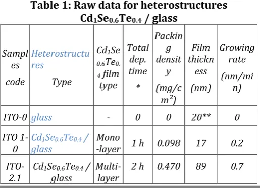
3.2 Film Thickness
Chemical Bath technique was adapted for multilayer Cd1Se0.6Te0.4/glass and samples with 1, 2 and 4 consecutively
deposited were prepared and characterised. Composition of the as prepared heterostructures, packing density, growing rate and thickness ofCd1Se0.6Te0.4films are presented in
table 1. The increase of Cd1Se0.6Te0.4/glass film thickness
with the total deposition time could be noticed. Moreover, for the same deposition time, the multilayer film is almost 7 times thicker then the corresponding monolayer one [19]. The use of a high number of successively deposited layers (coatings) determines the increase of the film thickness [19]. One can note that for various heterostructures, the growing rate is different, increasing with the number of coatings.
Table 1: Raw data for heterostructures
Cd
1Se
0.6Te
0.4/ glass
Sampl es code
Heterostructu res
Type
Cd1Se 0.6Te0. 4 film
type Total
dep. time *
Packin g densit
y (mg/c
m²)
Film thickn
ess (nm)
Growing rate (nm/mi
n)
ITO-0 glass - 0 0 20** 0
ITO
1-0 Cdglass 1Se0.6Te0.4/ -layer Mono 1 h 0.098 17 0.2
International Educational Applied Research Journal
Volume: 2 | Issue: 1 | Jan 2018
3
INTERNATIONAL EDUCATIONAL APPLIED RESEARCH JOURNAL
ITO2.
3 Cd1Seglass 0.6Te0.4 / 4 h 1.434 243 1.3
Key: * where: n = number of layers, m = deposition time; **- manufacturer measurement
3.3 Optical Transmittance
The transmission spectra of the heterostructures that contain multilayer Cd1Se0.6Te0.4/glass films illustrates the
decrease in film transparency parallel with increases in film thickness (fig. 1). As opposed to post treated films, there seems to be an increase film transmittance (fig. 2). It can be noted that the glass substrate shows a high transparency on the entire visible domain.
300 400 500 600 700 800 900 1000
0 20 40 60 80 100 ITO 2.3 ITO 2.1 ITO 1.0 ITO 0 T ran sm itan ce( %) Wavelength (nm)
Figure 1: Transmittance in multilayered
Cd
1Se
0.6Te
0.4/ glass film
300 400 500 600 700 800 900
0 20 40 60 80 100 ITO 2_3TT ITO 2_3 ITO 0 Wavelength (nm) T ran sm itan ce %
Figure 2: Transmittance in Cd1Se0.6Te0.4 / glass after
the thermal treatment
3.4 X-ray diffraction
The X-ray diffraction were used to investigate the optical and structural properties of different Cd1Se0.6Te0.4/glass
hetero-structures (fig. 3 and fig. 4). The crystalline structure of thermally treated Cd1Se0.6Te0.4/glass heterostructures was
investigated by X-ray diffraction and characteristic bands of the hexagonal crystalline structure [20] of the cadmium selenide could be noticed as depicted in fig. 3.
25 30 35 40 45 50 55
0 500 1000 1500 2000 2500 3000 3500 24 .85 26 .5 28 .2 31 .05 35 .9 38 .2 43
.95 45.8
51 .45 53 .05 58 .3 67 .2 ITO ITO ITO ITO CdS CdS CdS CdS CdS ITO
Diffraction angle 2 [degree] ITO 2.1TT In te ns ity [a .u ]
Figure 3. XRD spectra for Cd
1Se
0.6Te
0.4/ glass
after the thermal treatment
It was also noted that the crystallinity of the films were high as a result of post-growing thermal treatment. Therefore, in order to compare the effect of multiple layers on crystalline structure observed, the XRD spectra were first normalised in rapport with (222) peak of the indium-tin oxide as shown in fig. 4. The spectra normalisation was used to input in evidence of the increase of the three XRD characteristic bands observed in Cd1Se0.6Te0.4 / glass i.e. (100), (002),
(101). This observation was attributed to the presence of a higher Cd1Se0.6Te0.4 crystal amount on the surface of glass.
23 24 25 26 27 28 29 30 31 32 33 34 35 36 37 38 39 40 0 20 40 60 80 100 120 CdS (101) CdS (002) CdS (100) ITO (411) ITO (400) ITO (222) In te ns ity [a .u ]
Diffraction angle 2 [degree]
ITO 2_1TT ITO 2_3TT
Figure 4. XRD spectra for Cd
1Se
0.6Te
0.4/glass with
multilayer CdS films
4. CONCLUSION
Thin films of Cd1Se0.6Te0.4 were synthesized using special
CBD. It proved to be a convenient deposition method since its films were well adhered to and were also homogeneous films with controllable thickness onto the glass substrate. Powder X-ray analysis confirmed the fundamental diffraction patterns of Cd1Se0.6Te0.4. UV-Vis and XRD
investigation illustrated the quality of the as prepared Cd1Se0.6Te0.4 hetero-structures as determined, from X-ray
International Educational Applied Research Journal
Volume: 2 | Issue: 1 | Jan 2018
4
INTERNATIONAL EDUCATIONAL APPLIED RESEARCH JOURNAL
on average by 1.4 and 0.6% from the mean measured intensity, attesting to the high internal consistency of measurements from extended-face crystals. By comparing data obtained from all its samples their average deviation from the mean to be 0.9%.
ACKNOWLEDGEMENTS
The authors acknowledge the support given by Dr. Walter Kamande Njoroge of Kenyatta University in performing the XRD spectra and Mr Maera John of Maasai Mara University fo performing transmittance measurements.