Download complete issue: Vol. 2, No. 1 (PDF)
9
0
0
Full text
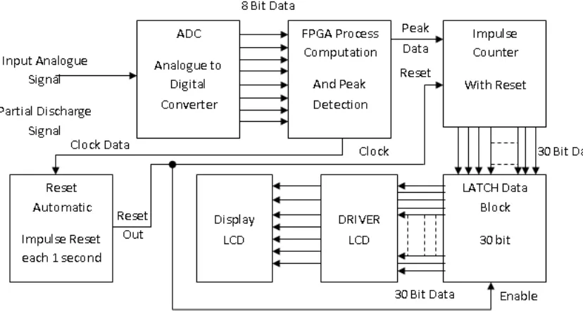
(2) 30. INTERNETWORKING INDONESIA JOURNAL. EMILLIANO ET AL.. Fig. 2 All Schematic Diagram of Block Diagram Partial Discharge Detection using FPGA. The function of ADC is to convert analogue signals to digital signals by sampling time, and digitize signal. FPGA with ADC is used as the real board integrates these two components. The purpose of the FPGA and the ADC converter is for counting the amount of PD signals from ADC signal in the FPGA and then perform the computation of the real time data using intelligence algorithm in VHDL Programming. Fig. 3 shows the input PD signals.. A7 A6 A5 A4 A3 A2 A1 A0 (5 Volt) FF = 1 1 1 1 1 1 1 1 ............................................. ............................................. (0 Volt) FF = 0 0 0 0 0 0 0 0 Fig. 5 Output Data in ADC Block. A.2. Process Convert PD Signal Data in ADC: OUTPUT BPF. (Band Pas s. Hex CC 00 7F. Filter) methode Eliptic s. 00 FF 33. 6F. FF 00 6F. Data Convert: 1 Volt = 33 hex 2 Volt = 66 hex 3 Volt = 99 hex 4 Volt = CC hex 5 Volt = FF hex. Fig. 3 Input Data Analogue from ADC Fig. 6 Output Data of ADC Block in Hexadecimal. Equation: X Volt =. A.1. Block Diagram ADC:. dec = convert to hex ….. (1). Fig. 4 shows the block diagram data ADC. A.3. Data input Partial Discharge in Binary Data: OUTPUT ADC (bin):. Fig. 7 shows the output data of ADC block in binary digital. (PORT A; 8 bit). OUTP UT. BPF. (B and. P as s. Filt er). met hode. E lipt ic s. Fig. 4 Block Diagram Data ADC. Fig. 5 shows the output data in ADC block. There are 256 levels to convert Analogue Data to Digital Data when process conversion data from 0 Volt to 5 Volt. OUTPUT Data in ADC Block:. Hex CC 00 7F. 00 FF 33. 6F. Bin: A7 1 0 A6 1 0 A5 0 0. 0 0 0. 0 1 1. ISSN: 1942-9703 / © 2010 IIJ. 0 1 1. 1 1 1. 0 0 1. FF 00 6F. 1. 0 0 1 0 1 1 0 1.
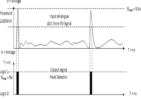
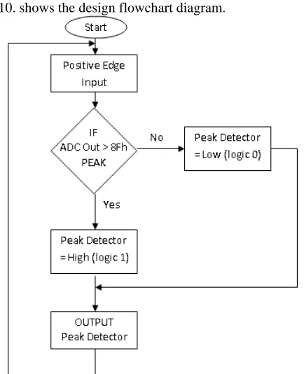
(3) INTERNETWORKING INDONESIA JOURNAL. Vol.2/No.1 (2010) A4 A3 A2 A1 A0. 0 1 1 0 0. 0 0 0 0 0. 1 1 1 1 1. 0 0 0 0 0. 1 1 1 1 1. 1 0 0 1 1. 0 1 1 1 1. 31. 1 0 0 1 0 1 1 0 1 1 0 1 1 0 1. Fig. 7 Output Data of ADC Block in Binary digital. A.4. Design ADC and PEAK Detection in FPGA: The function of this peak detector is for detect peak signals PD from sensor. In this simulation the peak detector is designed to have a 2.8 V = 8F hex threshold voltage. It means that if the input signal is more than 2.8 V or 8F hex, the output of the peak detector is logic 1 or 5 V and if input signal is less than 2.8 V or 8F hex, the output peak detector is logic 0 or 0 V. Detail of simulation model of Peak detector is shown in Fig.8. A.5. Block Diagram Simulation Model FPGA for ADC and PEAK Detection:. Fig.10. Design Threshold and Process Peak Detection. Fig. 9 shows the design threshold for input data analogue of ADC block in peak detector. Fig.10. shows the design threshold and output data of peak detector. A.7. Comparator between design VHDL and Verilog Programming for ADC and PEAK Detection block in FPGA: A.7.1. VHDL Programming:. Fig. 8 Simulation Model FPGA of ADC and PEAK Detector using VHDL Programming. Comparator : ( Threshold = 8F hex = 2.803 Volt ) Threshold is designed in value 2.803 Volt or 8F hex to detect PD signals in peak detector block. Output of peak detector is logic high (logic 1=5V), if the input peak detector block is more than 8F hex or if input ADC block is more than 2.803 Volt. Output of peak detector is logic low (logic 0=0V), if the input peak detector block is less than 8F hex or if input ADC block is less than 2.803 Volt. A.6. Design Threshold for ADC and Peak Detector Block: Design Threshold for Analogue Signal of Input Partial Discharge Signal:. library IEEE; use IEEE.STD_LOGIC_1164.ALL; use IEEE.STD_LOGIC_ARITH.ALL; use IEEE.STD_LOGIC_UNSIGNED.ALL; entity ADCandPEAK is Port ( CLOCK : in STD_LOGIC; ADC : in STD_LOGIC_VECTOR (7 downto 0); PEAK : out STD_LOGIC); end ADCandPEAK; architecture Behavioral of ADCandPEAK is signal PEAK_DETECT : std_logic := '0'; begin process (CLOCK) begin if (CLOCK'event and CLOCK ='1') then if (ADC > "10001111") then PEAK_DETECT <= '1'; else PEAK_DETECT <= '0'; end if; end if; end process; PEAK <= PEAK_DETECT; end Behavioral;. A.7.2. Verilog Programming module ADCandPEAK(CLOCK, ADC, PEAK); input CLOCK; input [7:0] ADC; output PEAK; reg [0:0] PEAK = 1'b0; reg [7:0] threshold = 8'h8F; //or threshold = 8'b1000_1111;. Fig. 9 Design Threshold for Input Data Analogue from ADC. always @(posedge CLOCK) if (ADC > threshold). ISSN: 1942-9703 / © 2010 IIJ.
(4) 32. INTERNETWORKING INDONESIA JOURNAL PEAK <= 1'b1; else PEAK <= 1'b0;. Endmodule. Listing programming A.71 shows the design VHDL programming for ADC and Peak detector block in FPGA technology. Listing programming A.72 shows the design Verilog programming for ADC and Peak detector block inn FPGA technology.. EMILLIANO ET AL.. 5. Input data 5th impulse from ADC is: 0010 0000 or 20 hex (0.62 V). 6. Input data 6th impulse from ADC is: 0000 1000 or 08 hex (0.157 V). 7. Input data 7th impulse from ADC is: 0000 0010 or 02 hex (0.039 V).. A.8. Flow Chart Diagram for ADC and PEAK Detection Programming: Fig.10. shows the design flowchart diagram.. Fig.12. Design Input Data Analogue PD signal for ADC and Peak Detection Block. A.10. Design Platform FPGA for ADC and PEAK Detector Block: Platform programming is VHDL (Very high speed integrated circuit Hardware Description Language) and Verilog programming. Platform FPGA is: 1. FPGA Virtex 5 (ML501 Board) 2. Chipset FPGA is XC5VLX50 3. Package of Chipset is FF676. Fig. 11 shows the design flow chart diagram for ADC and peak detector block in FPGA.. Design clock timing in FPGA Xilinx Virtex 5 is: 1. Clock High Time is : 20 ns 2. Clock Low Time is : 20 ns 3. Input setup Time is : 10 ns 4. Output Valid Delay is : 10 ns 5. Offset is : 100 ns 6. Initial Length of Test Bench is : 1000 ns. A.9. Design Input Data Analogue ADC for Simulation PD signal in ADC and PEAK Detector of FPGA:. A.11. Result Test Simulation for ADC and Peak Detector Block Programming:. Fig.11. Design Flow Chart Diagram for ADC and Peak Detection Block in FPGA. Fig.12 shows the design input PD signal to FPGA board from ADC board before simulation VHDL using Xilinx ISE simulator. Design input data before simulation as follow: 1. Input data 1st impulse from ADC is: 1110 1111 or EF hex (4.686 V). 2. Input data 2nd impulse from ADC is: 0000 0000 or 00 hex (0 V). 3. Input data 3rd impulse from ADC is: 1101 1111 or DF hex (4.372 V) 4. Input data 4th impulse from ADC is: 1011 1111 or BF hex (3.745 V). Fig.13. Simulation Model FPGA of ADC and Peak Detector Block using Test Bench Wave ISE Simulator from 0 ns until1000 ns. ISSN: 1942-9703 / © 2010 IIJ.
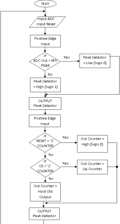
(5) INTERNETWORKING INDONESIA JOURNAL. Vol.2/No.1 (2010). A.11.1 Analysis Graphic:. 33. B.2. Block Diagram:. Fig.16. Block Diagram Design for 30 bit Counter and Reset Block in FPGA. Fig.14. Analysis Simulation Model FPGA of ADC and Peak Detector Block Programming.. Result Test in fig.13. shows the peak detector can detect Peak of PD signal from input signal ADC. The Peak detector in this simulation is designed to have a 2.803 V = 8F hex threshold voltage. It means that if the input signal is more than 2.803 V or 8F hex, the output of the peak detector is logic 1 or 5 V and if input signal is less than 2.803 V or 8F hex, the output peak detector is logic 0 or 0 V. Detail of simulation model result of Peak detector is shown in Fig.14.. Fig.16. shows the design 30 bit up counter with reset in FPGA. OUTPUT Data in Counter and Reset Block: A29 A28 A27..... A3 A2 A1 A0 3FFF FFFF = 1 1 1 ..... 1 1 1 1 ----------------------------------------------------------------0000 0000 = 0 0 0 ...... 0 0 0 0 There are 1,073,741,824 levels counting to count Digital PD signal Data from Peak detector when process counting data from 0000 0000 hex to 3FFF FFFF hex.. A.11.2 Conclusion of the Simulation: This ADC and PEAK Detection Block has been successful to be running in FPGA Programming. B. Block Counter and Reset : B.1. Design Counter and Reset Block: The purpose of the Counter and Reset Block is for counting the amount of PD signals from ADC signal and Peak detection Block in the FPGA and then perform the computation of the real time data using 30 bit digital Output data in VHDL Programming. So it means counter will run up counter from 0 to 1,073,741,824 counting or 0000 0000 hex to 3FFF FFFF hex counting. Counter will return back to 0 if the reset of counter is active. In this VHDL programming, counter is designed using reset active high (type negative edge reset) for Up Counter in FPGA. Fig.15. shows the input data analogue from ADC.. Fig.17. Block Diagram Design for 30 bit Counter and Reset Block in FPGA. Fig.17 shows desire result from design counter with reset block programming. The desire result have to show the output up counter increase when there is impulse signal, and the output up counter must be zero when the reset signal is active. B.3. Flow Chart Diagram for Counter and Reset Block Programming:. Digital Signal of Input Counter and Reset Block in FPGA:. OUTPUT BPF. (Band. Pas s. Filt er). met hode. Elipt OUTPUT ic s BPF (Band Pass Filter) methode Eliptics. Fig.15. Input Data Analogue from ADC. Fig.18. shows the design flowchart diagram of Counter and Reset Block in FPGA. The first time program of counter is setting to positive edge input. The second step of the program is select data input, if the input reset data is active or logic high then the output counter must be reset to zero value. If the input reset data is not active or logic low, the program will continue the next step. The third step of the program is select input data of CE (chip enable). If the CE is given data active or logic high then the output data counter must be increase data by 1. If the CE is not active then data output counter must be the same with old data. So data output counter will be stop if CE is not active and the counter will run again after the input CE is active again.. ISSN: 1942-9703 / © 2010 IIJ.
(6) 34. INTERNETWORKING INDONESIA JOURNAL. EMILLIANO ET AL.. counter is running depend of amount impulse Peak Detector from input Counter and Reset Block. If there is impulse reset is active in 600 ns, the counter is return back to 0 and do up counting again. B.4.2. Conclusion of the Simulation: The Up Counter and Reset Block has been successful to synthesis, compile, simulate and run in FPGA Programming. C. Combination ADC-Peak Detection and Counter-Reset Block C.1. Design Peak Detector and Up Counter Block: The counter will reset each 1µs, and the data output will be hold by a latch for display purpose. The data will be updated to display each 0.5µs or 500ns in FPGA. For constant impulse signal rate, there will be 108 Impulse in 1 second if there is 1 impulse in each 10 ns. In real system data will be updated to display each 1second in FPGA. C.2. Block Diagram of Peak Detector and Counter:. Fig.18. Design Flow Chart Diagram for Counter and Reset Block in FPGA. B.4. Result Test Simulation for Counter and Reset Block Programming:. Fig.21.Simulation Model FPGA of Peak Detector and Up Counter Block using Test Bench Wave ISE Simulator Fig.19. Simulation Model FPGA of Counter and Reset Block using Test Bench Wave ISE Simulator from 0 ns until 230 ns. Fig.21. shows the simulation model FPGA of peak detector and up counter with reset block. Design clock timing in FPGA Xilinx Virtex 5 for simulation model FPGA of peak detector and up counter with reset block is:. Fig.20. Simulation Model FPGA of Counter and Reset Block using Test Bench Wave ISE Simulator from 500 ns until 700 ns. B.4.1. Analysis Graphic: Fig.20 and 21 shows the up counter is running from 0 to 46 hex when Reset is not active and Chip Enable is active. Up. 1. 2. 3. 4. 5. 6.. Clock High Time is : 5 ns Clock Low Time is : 5 ns Input setup Time is : 2 ns Output Valid Delay is : 2 ns Offset is : 100 ns Initial Length of Test Bench is : 1000 ns. C.3. Flow Chart Diagram for Combination ADC with Peak Detector Block and Counter with Reset Block Programming:. ISSN: 1942-9703 / © 2010 IIJ.
(7) INTERNETWORKING INDONESIA JOURNAL. Vol.2/No.1 (2010). 35. Fig.23. Simulation Model FPGA of ADC and PEAK Detector using Test Bench Wave ISE Simulator. A.2. Result Test: Table 1. Data Result Test Peak Detector. The data experiment lab of simulation VHDL programming shows output peak detection is logic high when the input voltage more than 2.803 volt. A.3. Analysis Graphic: Fig.22.Simulation Combination Peak Detector Block and Counter Block. Fig.22. shows the design flowchart diagram of Combination ADC with Peak Detector Block and Counter with Reset Block in FPGA. III. SIMULATION RESULT A. Test Simulation FPGA using Test Bench Wave for ADC and PEAK Detection Programming: A.1. Simulation Result Graph: Fig. 23 shows the result test simulation model of ADC and Peak Detector block programming. Table.1 shows the data result of simulation test of ADC and Peak Detector block programming. Fig.24 shows the analysis graphic of simulation ADC and Peak Detector block programming.. Fig.24. Analysis Graphic of Simulation Model FPGA for ADC and PEAK Detector Block. B. Simulation FPGA for Combination ADC with Peak Detector Block and Counter with Reset Block Programming. ISSN: 1942-9703 / © 2010 IIJ.
(8) 36. INTERNETWORKING INDONESIA JOURNAL. B.1. Simulation Result:. EMILLIANO ET AL.. there is impulse reset is active in 500 ns, the counter is return back to 0 and do up counting again. The up counter is counting when there is input analogue PD signal from ADC that more than threshold line 2.803 Volt or 8F hex. The up counter will return to zero (0) again if reset is active (the reset is active high). V. CONCLUSSION Result Test show that Output Peak Detector can detect Peak signal from input signal ADC. The Peak detector in this simulation is designed to have a 2.803 V = 8F hex threshold voltage. It means that if the input signal is more than 2.803 V or 8F hex, the output of the peak detector is logic 1 or 5 V and if input signal is less than 2.803 V or 8F hex, the output peak detector is logic 0 or 0 V. This ADC and PEAK Detection Block has been successful to be running in FPGA Programming. The ADC-Peak Detector and Up Counter-Reset Block has been successful to synthesis, compile, simulate and run in FPGA Programming. Combination ADC-Peak-Counter can work successfully.. Counter Fig.25. Test Simulation FPGA for Peak Detector and Up Counter Block using Test Bench Wave. VII. REFERENCE [1] Ahmad Basri bin Abdul Ghani, “Detection of Partial Discharge in Underground Cable Using Magnetic Probe,” in 2008 Doctoral Thesis in University Tenaga Nasional, Malaysia, 2008.. B.2. Analysis Graphic:. [2] A. Morgado, V.J. Rivas, R. del Rio, R. Castro-Lopez, F. Fernandez and J.M de la Rosa, ”Behavioral Modeling, Simulation and Synthesis of Multi-standard Wireless Receivers in MATLAB/SIMULINK” VLSI Journal 2008, Vol.41. [3] Bill Schwartz, Michael Carfore, and Dr. Robert Qiu, “Ultra Wideband Transmitter & Receiver Design,” in The REU Program of Tennessee Technological University, July 27, 2005. [4] Benjamin Nicolle, Mourad Zarour, William Tatinian, Gilles Jacquemod, “System Design Oriented Low Noise Amplifier Modeling” in IEEE 2007 [5] S. Braun, F. Krug, and P. Russer, “A novel automatic digital quasi-peak 60detector for a time domain measurement system,” in 2004 IEEE InternationalSymposium On Electromagnetic Compatibility Digest, August 9–14, Santa Clara, USA, 2004. [6] CISPR16-1, Specification for radio disturbance and immunity measuring apparatus and methods Part 1: Radio disturbance and immunity measuring apparatus. International Electrotechnical ommission, 1999.. Fig.26. Analysis Graphic Signal for Peak Detector and Up Counter Block in Simulation FPGA. Fig.25 shows the result test of simulation combination ADC with peak detector block and counter with reset block programming in VHDL. Fig.26 shows the analysis graphic signal of combination ADC with peak detector block and counter with reset block. Fig.25 and 26 shows the up counter is running from 0 to 5 hex when Reset is not active and Chip Enable is active. Up counter is running depend of amount impulse Peak Detector from input Counter and Reset Block. If. [7] L. Cohen, “Time-Frequency Distributions - A Review,” in Proceeding of the IEEE, vol. 77, no. 7, pp. 941–981, 1989.[4] A. V. Oppenheim and R. W. Schafer, Discrete–Time Signal Processing.ISBN 0-13-214107-8, Prentice-Hall, 1999. [8] M. S. Chong, “Partial Discharge Mapping of Medium Voltage Cables – TNB’s Experience”, CIRED 2001, 18-21 June 2001, Conference Publication No. 482 © IEEE 2001 [9] F.H Kreuger, “Discharge Detection in High Voltage Equipment”, A Heywood Book, Temple Press Book Ltd, London 1964. [10] Xilinx Tutorial Documentation, “ISE 9.1i Quick Start Tutorial”, Copyright © Xilinx, Inc. All rights reserved, 1995-2007.. ISSN: 1942-9703 / © 2010 IIJ.
(9) INTERNETWORKING INDONESIA JOURNAL. Vol.2/No.1 (2010) Emilliano. S.Pd First degree in Electrical and Electronics (University Negeri Jakarta, Indonesia), 2001 M.T. Master Engineering in Department of Electrical Engineering in Control Engineering LSKK-EE-ITB (Bandung Institute of Technology, ITB), 2005 E-Mail: [email protected] Telephone: +60 3 89212020 ext. 3288 Office: BW-4R-015 Area of Research: Automatic Real Time System of Partial Discharge Detection for Under Ground Cable Using Giga Hertz Speed Data Acquisition and Xilinx FPGA Technology in VHDL Programming.. Assoc. Prof. Dr. Chandan Kumar Chakrabarty MIMM, InstP, CPhys, CEng Ph. D. (RF Plasma Technology) (Flinders Univ., Australia), 1996 M.Sc. (Pulsed Plasma Technology) (Univ. of Malaya, Malaysia), 1988 B. Sc. (Hons.) in Physics (Univ. of Malaya, Malaysia), 1986. E-Mail: [email protected] Telephone: +60 3 8921 3230 Office: BW-2-C030 Area of Specialization / Research Interest: Radio Frequency and Microwave Technology, Gas Discharge Physics. Dr Agileswari K. Ramasamy Ph. D. in Electrical Engineering (Univ. Tenaga Nasional, Malaysia) M. Sc. in Control Systems (Imperial College, UK) B. Sc. in Electrical Engineering (Purdue Univ., USA) E-Mail: agileswari Telephone: +60 3 8921 2270 Office: BN-1-031. Dr . Ir. Ahmad Basri bin Abdul Ghani TNB Research Sdn. Bhd. As the Technical Manager for High Voltage Testing Laboratory. PhD in Electrical Engineering with split PhD program between Univ. Tenaga Nasional, Malaysia and University of Southampton, UK. Master in Engineering Management at Univ. Tenaga Nasional, Malaysia. B.Eng. (Hons) in Electrical Engineering at University of Southampton, UK. E-Mail: [email protected]. Note: An earlier version of this paper was presented at the ICA2009 International Conference in October 2009 in Bandung, Indonesia.. ISSN: 1942-9703 / © 2010 IIJ. 37.
(10)
Figure

+2
Related documents
innovation in payment systems, in particular the infrastructure used to operate payment systems, in the interests of service-users 3.. to ensure that payment systems
The approach taken was to design, build and test two different versions of our basic approach: a genetic program which digs out relevant trading signal information from tick
The next step in the postprocessing is to plot the contours of the von Mises stress using the von Mises Stress icon in the Image toolbar.. The von Mises stress is displayed to the
On the cutting paper task, Bryan completed 10.7% more steps correctly when viewed from the POV perspective, and 12.6% and 19.3% more steps correctly in the POV perspective on the
This section of the paper addresses the following topics: (1) culturally responsive teaching; (2) building vocabulary; (3) a cognitive method based on active thinking; (4) a
Hull appendages, rigs and sails are measurement controlled. Raceboard hulls may, after having left the manufacturer, only be altered to the extent permitted in Section C of the
Supervised by faculty with expertise in R&D of fuel cells, power electronics, solar energy, and thermal energy, the students were able to gain practical skills for fabricating
