Of Multilayer Films by X-Ray Diffraction
M.R. Behfrooz
*Department of Physics, Islamic Azad University of Mahabad, Mahabad, Islamic Republic of Iran
Abstract
X-ray diffraction measurements were performed on Co
αPt
1-α/Pd, Co/Pd, Co/Fe,
and Co/W multilayer samples with different structures, such as Co
αPt
1-αalloy
layer composition α, bilayer thickness, and number of bilayers. Multilayer
samples were made by magnetron sputtering in a chamber with multi-parallel
guns and a position controllable substrate. Co
αPt
1-αalloy layers were deposited by
cosputtering from Co and Pt targets mounted on guns tilted towards a common
substrate. Compositions of Co and Pt in Co
αPt
1-αlayers were varied by use of
different sputtering power. The thicknesses of magnetic and non-magnetic layers
in multilayered samples were also systematically changed to investigate the
relationship between X-ray diffraction lines and crystalline structures of
multilayered films. It was found that the position of the main diffraction peak
from multilayered films was solely determined by the crystalline structures within
bilayers rather than bilayer thickness. A model was introduced to calculate
microstructural parameters such as the thickness of interfaces and compositions at
interfaces.
Keywords: Multilayer films; X-Ray diffraction; CoαPt1-α/Pd; Co/Pd; Co/Fe; Co/W
*
E-mail: mr.behfrooz@mail.urmia.ac.ir Introduction
Multilayered films fabricated in different deposition systems, such as molecular beam epitaxy, electron beam evaporation, and magnetron sputtering, have attracted much attention in the last decade because of their novel magnetic, optical, and mechanical properties [1,2]. Particularly due to the application to high density magneto-optic recording media, magnetic multilayers of Co/Pt and Co/Pd [3-7] have been intensively studied. In the last few years, more than 20 non-magnetic materials making up multilayers with either Co or Fe have been investigated world wide. Of these materials, (Co or Fe)/(Pt, Pd, Au, Ag, Cu, Cr, Dy, Gd, or Tb) are the most
popular. In order to get perpendicular magnetic anisotropy which is crucial for magneto-optic recording media, the thickness of magnetic layers (Co or Fe) is limited to about 3Å. Therefore, powerful micro-structural analysis tools such as high resolution electron microscopy (HRTEM) are necessary to study nano-structures of multilayers. However, in most cases, because the interesting regions in multilayered systems are interfaces which are no more than 10Å thick, one may not be able to obtain details of the nano-structure of these multilayers, even with HRTEM.
fabrication techniques, artificial structures have been the focus of many research groups. These developments challenge the XRD technique, and new interpretations of XRD data are required. Lots of works have been done on XRD from multilayered systems by many groups such as Fullerton and Schuller et al [8]. But because in XRD only the scattered X-ray intensity is measured and the phase information is totally missing, modeling is usually required to fit the measured intensity, and thus indirectly, the structures of samples may be obtained. The problem with modeling is that fits are not unique.
In general, low angle XRD from multilayered structures has been fairly well understood, and at least qualitative descriptions of structures can be determined. Fullerton et al. [8] have successfully built models that fit low angle X-ray diffraction patterns, as well as large angle XRD patterns, to get information on layer interface sharpness. However, the interpretation of wide angle peaks remains unclear in some cases, especially for ultra-thin sublayer multilayers, and there still exist many open questions. In particular, positions of wide angle peaks appear to be in question when they are used to interpret crystalline structures, because the position of peaks may be changed by the artificial layering. Therefore crystalline structures and material phases in multilayered films may not always be directly found from wide angle XRD patterns alone.
For one-dimensional ideal superlattices where all the atomic layers are parallel and there are no interdiffusions and no layer thickness fluctuations the following model describes the diffracted X-ray intensity from the superlattices [13,14]:
2 1 1 2
0 1 1 2 2 2 2 2
1 2 1 2
1 1 2 2
1 2
sin( / 2)
sin( / 2)
( ) [( )
sin( / 2) sin( / 2)
sin( / 2)
( )
sin( / 2)
2 cos( ( ))
2
sin( / 2) sin( / 2)
( ))]
sin( / 2) sin( / 2) n qd
NqL
I I f
qL qd
n qd f
qd
q
f f L d d
n qd n qd
qd qd
=
+
+ + −
where N is the number of bilayers; q is the wave vector;
d1(d2) is the lattice spacing of the first (second) sublayers; n1(n2) is the number of atomic planes in the first (second) sublayer; f1(f2) is the atomic scattering factor of the first (second) sublayer. For multilayers consisting of ultra-thin sublayers (3-20Å) with many bilayers, the first term in the above equation dominates, and the positions of all diffraction peaks are basically
determined from this term. However, for multilayers made in sputtering and thermal evaporation systems, interdiffusions at interfaces are unavoidable and alloys may form at interfacial regions. Furthermore, layer thickness fluctuation is another factor that can eliminate the superlattice effects for XRD peaks at large angle [9,10]. This study was conducted in order to study systematically this problem and, thus, to obtain a clear understanding of how the structures (including layer thickness, number of layers, and interdiffusivity between layers) influence the diffraction results.
There are many samples made for this study. In sections §1 and §2, we report on multilayers with different layer structures and different interfacial crystallinities, and study crystalline structures of these films. In section §3, a simple model is employed to determine microstructural parameters, such as interface thickness and composition at interfaces, based on measured quantities such as bilayer thickness and film composition. These microstructural parameters, in general, are not easy to be directly measured. We found that the model is useful in the sense that important parameters such as local composition and relative atomic number density may be estimated. As mentioned above, XRD alone may not always yield unique and complete solutions to all the microstructural parameters. Other independent measurements must be made to uniquely determine these parameters. We found that for Co/Pd multilayers, magnetic measurements were helpful for the determination of microstructural parameters. Magnetic measurement data are presented in section §4. More detailed study on magnetic properties of some of these samples has been carried out and will be published elsewhere.
Experimental
Multilayers were grown in a multi-gun magnetron sputtering system with each gun oriented in an upward direction and a substrate positionable above the desired gun. Base pressure of the system was 5xl0-8 Torr. Sputtering pressure was 5 mTorrof Argas. The CoαPt1-α alloy layers were fabricated by cosputtering from Pt and Co targets which were tilted at an angle so that Pt and Co would be deposited simultaneously on the substrate.
number of bilayers τwas changed from 10 to 40, and the bilayer structure was kept the same: Co0.2Pt0.8 (21Å)/Pd(3.3Å). In Group IV, the thickness of Pd sublayers γ was changed from 3.3 to 19.8Å with other parameters fixed: Co0.2Pt0.8(21Å)/Pd(γÅ)x20.
The structural parameters of these samples are summarized in Table 1. Alloy films CoαPt1-α with α ranging from 20 atomic percent Co to 28 atomic percent Co were also made for comparison purpose. Conventional θ-2θ X-ray diffraction was performed and both small and large angle scans were taken.
For samples of Co/Pd (Group V), Fe/Pd(Group VI), and Co/W(Group VII) multilayers, the thicknesses of the Co or Fe layers varied from a fraction of one mono-layer(lÅ nominally) to about 4Å. The nonmagnetic layers such as Pd and W had fixed layer thickness of 13Å, as shown in Table 2. There were seven samples in each group. Because of the different diffusivity between Co-Pd, Fe-Pd, and Co-W, these three groups were made for the study of the interdiffusion and its effect on XRD patterns.
There were two other sample groups (VIII and IX). These were used to test a model that relates micro-structural parameters, such as interfacial thickness, to measurable quantities such as bilayer thickness and over-all composition. The sample structural parameters are listed in Tables 3 (Group VIII) and 4 (Group IX). The bilayer thickness λ of these samples and the over-all composition of Co x were determined from small angle XRD and EDS, respectively.
Results and Discussion
§1. CoαPt1-α/Pd Multilayers
In this section, XRD results from multilayers made with CoαPt1-α alloy layers and Pd layers will be discussed. The structures of these samples can be found in Table 1.
In sample group I of CoαPt1-α/Pd multilayers, the composition of the Co in CoαPt1-α sublayers varies from 8.5 atomic percent to 36 atomic percent. Small angle XRD patterns from these samples reveal that the bilayer thickness of the samples is about 24Å compared with the nominal thickness of about 20Å. Up to the third order for small angle peaks are visible for these samples. From this information, it can be concluded qualitatively that these samples have similar layered structures or chemical modulation. In the large angle region, there are a few peaks visible: peaks labeled (111), (200), (311), and (222) as shown in Figure 1 for CoαPt1-α/Pd with α=0.085 (sample I-1). The (220) peak is also clearly visible for samples with Co concentration
Table 1. The general structure is [CoαPt1-α(βÅ)Pd(γÅ)]xτ.
The parameters in parentheses indicate the variable parameters of the groups. Parameters assigned values indicate fixed parameters in the group
Sample Group I(α) Group II(β) Group III(τ) Group IV(γ) number β=17 α=0.2 α=0.2 α=0.2
γ=3.3 γ=3.3 β=21 β=21
τ=20 τ=20 γ=3.3 τ=20
1 0.085 9 10 3.3
2 0.159 13 15 6.6
3 0.195 17 25 9.9
4 0.255 21 30 13.2
5 0.283 25 35 16.5
6 0.359 29 40 19.8
Table 2. Co/Pd (Group V), Fe/Pd (Group VI), and Co/W (Group VII) multilayer sample groups. In each group, the non-magnetic sublayer (Pd or W) is 13Å thick nominally, and the thickness of the magnetic sublayer (Co or Fe) varies from a fraction of one mono-layer (1Å) to about two atomic layers (4Å)
Sample number 1 2 3 4 5 6 7
λFe or λCo(Å) 1 1.5 2 2.5 3 3.5 4
Table 3. Sample (Group VIII) structures of Co(2Å)/ Pd(λPd)x35 multilayers. The bilayer thickness λ and over-all
composition of Co x were measured using small angle XRD and energy dispersive spectroscopy
Sample number 1 2 3 4 5 6 7
λPd(Å) 4 7 10 13 16 19 21
λ(Å) 6.6 10.1 13.1 15.5 18.9 21.2 24.9
CoxPd1-x 0.37 0.24 0.18 0.15 0.13 0.11 0.10
Table 4. Sample (Group IX) structures of Co(4Å)/Pd(λPd)
with total film thickness of about 300Å. Bilayer thickness λ and Co composition x were measured using small angle XRD and EDS
Sample number 1 2 3 4 5 6
λPd 4 8 12 16 20 24
No. of bilayers 37 25 18 15 12 10
a less than 25 atomic percent. The position of these peaks varies corresponding to the change of Co concentration α, as shown in Figure 2. These large angle peaks clearly reveal polycrystalline fcc structures with differing lattice parameters. In this case, the bilayer thickness has a negligible effect on the large angle peak positions. This may indicate that there does not exist strong coherence between layers, or as other groups have pointed out, [9,10] superlattice peaks do not exist when there are layer thickness fluctuations.
XRD patterns from samples of group II (see Table 1) show the same result (not shown) that the change of bilayer thickness has virtually no effect on the position of large angle peaks for these sputter deposited multilayer films. These results suggest that for Group II, chemical modulation of the films has no effect on the position of the large angle peaks. The intensity of these peaks increases with increase in layer thickness, as expected. The above results and discussions suggest that layered structures fabricated in sputtering system have little effect on positions of large angle peaks. Crystalline structures of films are the dominant factors determining large angle diffraction patterns.
XRD data from Groups III and IV show the same results from a different angle. Samples in group III have different number of bilayers, varying from 10 to 40. Group IV samples have different Pd layer thicknesses. The total film thickness, therefore, increases for samples in both Groups III and IV. The intensity of peaks increases accordingly. In general, the reflected X-ray intensity from (hkl) planes is proportional to the effective volume of the sample,[11] and in this case, proportional to the film thickness. In both sample groups III and IV, the intensity of (111) and (222) peaks increases faster than others, indicating that the preferred direction to grow is with (111) planes parallel to the film surface. Figure 3 shows the positions of the (222) peaks from samples in Group IV. It can be seen that although the Pd layer thickness increases from about 3Å to 20Å, the (222) peak does not move at all. It once again shows that chemical modulation length has little effect on the position of large angle peaks. Other results are that satellite peaks appear clearly when the nominal Pd sublayer is more than 10Å thick, as shown in Figure 4. For ideal multilayer structures, satellite peaks always exist, however, in practice, because of the layer thickness fluctuation of each individual layer, satellite peaks are visible only when thickness fluctuations are small compared with each individual layer thickness. Thus, the existence of satellite peaks may indicate small layer thickness fluctuations.
§2. Co/Pd, Fe/Pd, and Co/W
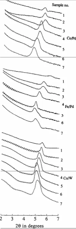
In this section, XRD from Co/Pd, Fe/Pd, and Co/W multilayers will be discussed. When two different materials are mixed together, there is always a certain type of solid state reaction between the two materials if they are miscible. It is expected that when multilayers are grown, alloy layers between layers could be formed. Therefore, interdiffusion between layers is a very interesting phenomenon. Samples listed in Table 2 have differing known interdiffusivity for these materials. These samples have about the same chemical modulation, as expected and shown by small angle
Figure 1. A typical large angle diffraction pattern from sample I-1. The peaks show that the film has fcc structure.
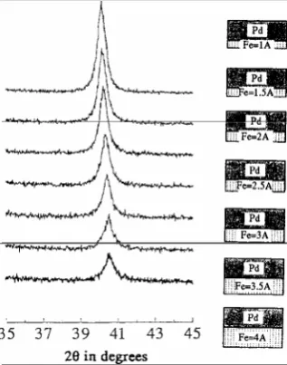
XRD scans in Figure 5, since they all have the same nominal structure. However, diffraction peaks from these samples at large angle behave differently. Figure 6 shows (111) peaks from Co/Pd samples with structures listed in Table 2. Notice that the peak shifts when the thickness of the Co layer increases, and that the peak intensity increases as well.
Figure 3. Diffraction patterns from (311) and (222) planes of samples in Group IV of Table 1. The peaks do not move when Pd layer thickness changes.
Figure 4. Satellite peaks show up on the right side of the main peak when the Pd layer thickness is more than 10Å. (Sample IV-3, Table 1).
On the other hand for Fe/Pd multilayers also listed in Table 2, the diffraction peak shifts just as for the Co/Pd samples, but the peak intensity goes down when the Fe layers are getting thicker and thicker, as shown in Figure 7. The change of the diffraction intensity is directly related to microstructure of thin films. The phase diagram of Co and Pd shows no intermetallic compound formation in the entire composition range. Instead, Co and Pd will form a solid solution at any composition of Co in Pd. However, Fe and Pd do have a chance to form an intermetallic compound such as FePd or FePd3. Therefore, the formation of compounds which may not be chemically ordered at interfaces may reduce the grain size, which will cause the diffraction peak broadening. The small shift of the peak position may be explained in two ways. One is that the d-spacing
detected is the average d-spacing of the two sublayers. When one layer is getting thicker, the average weight of the d-spacing of that layer will be greater. Thus, the detected d-spacing will move towards the value of that d-spacing. This explanation is valid for multilayers with rather thick sublayers. In that case, the layers are thick enough to grow with their bulk structures. Another explanation is that for multilayers containing ultrathin sublayers, such as the samples in this study, the two sublayers of a bilayer are only about several Å, or three to four mono-layers thick. For such a small amount of material, it is difficult to form structures the same as for bulk. For samples of either Co/Pd or Fe/Pd multilayers, because the similarity in crystallinity of Pd layers (fcc) and CoPd or FePd alloy layers (also fcc), it is impossible to draw any conclusion about crystalline structures in different layers. In fact, it is likely that the lattice structure of the two sublayers are the same, and entire film takes on the crystal structure of the thicker sublayer.
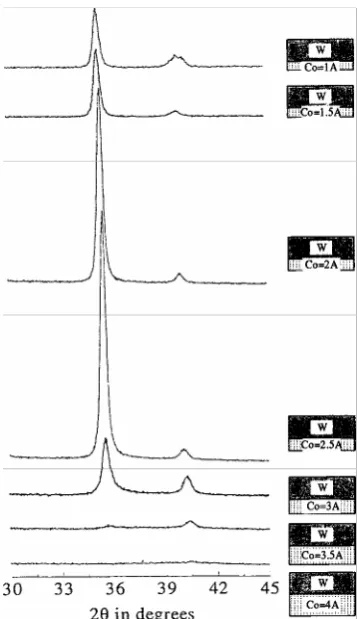
The lattice structure of W (bcc) is entirely different from that of CoW alloys which were made by co-sputtering, as shown in Figure 8. The XRD from sputter deposited W films shows the typical bcc structure. By adding about 10 at % Co in W, a different XRD pattern
Figure 6. Large angle XRD patterns from Co/Pd multilayers. Notice that the peak shifts and gets more intensive when Co layer thickness increases. (See Table 2).
shows up. Also, when the composition of Co increases, the intensity of the main peak reduces, and finally, the peaks disappear, as shown in Figure 8. The Co/W multilayers behave exactly the same as these CoW alloy films, as shown in Figure 9. The only difference is that the peak at about 2θ=40° is more intense for the multi-layers. Also when the Co layers get thick enough (>4Å), the entire film becomes amorphous.
Now, there are some difficulties explaining the Co/W XRD patterns using the idea of an average d-spacing, because the diffraction pattern from W does not have a peak around 2θ=35°. As a matter of fact, it is quiet clear
Figure 7. Large angle XRD patterns from Fe/Pd multilayers. Notice that the peak shifts and gets less intensive when Fe layer thickness increases. (See Table 2).
that the entire film of Co/W multilayers should possess the same lattice structure. So far, the type of lattice structure in either CoW alloy films or in Co/W multilayers has not been identified because there is not enough information. In order to get more diffraction peaks from these Co/W samples, and thus, to identify the phase, grazing incident angle X-ray diffraction may be useful [12]. From Co/W samples, it can be seen that interdiffusion between the Co and W sublayers is so significant that a trace (1Å) of Co will change the entire lattice structure. On the other hand, these Co/W multilayers are still chemically modulated, as shown in Figure 5.
From the above analysis and discussions of the microstructures of ultra-thin sublayer multilayers made by sputter deposition, it can be concluded that the entire film possesses the same lattice structure, but atoms of the two materials are distributed in such a way that chemical modulation still exists in the direction perpendicular to surface, as shown schematically in Figure 10.
Figure 9. Large angle XRD patterns from Co/W multilayers. Notice that the similarity of these patterns and those of CoW alloy films shown in Figure 8. (See Table 2).
As mentioned previously, a quantitative micro-structural description of multilayers with ultra-thin sublayers, such as samples in this study, is very difficult to obtain. Fittings to X-ray diffraction patterns usually ends up with more than one possible solution which may be equally physical. Therefore, more information from measurements other than XRD is required to uniquely determine microstructures. In order to make use of the information from other measurements, a relation between quantities obtained from XRD and that from other measurements is desired. To this end, we propose the following simple model which will lead to an equation relating quantities, such bilayer thickness and over-all composition of the entire film to microstructural parameters such as interracial thickness and local composition.
§3. Modeling of Interfaces
The model is shown schematically in Figure 11. The figure shows one of bilayers in a X/Y multilayer system containing materials X and Y. Sublayers a and b are determined in such a way that layer a contains both X and Y, and layer b contains only Y. In other words, layer a is the layer of X and Y mixture, and layer b is pure Y. After defining a few other parameters (such as local composition of X in layer a: x(X)a; and atomic numbers per volume in layers a and b: na and nb), the following equation is obtained:
Figure 10. A schematic of crystalline structure consisting of ultra-thin sublayers.
( ) ( )
11 a a
a a a
b b
n n
x X
n n x X
λ λ= ⎛⎜ − ⎞⎟+ λ
⎝ ⎠
where λ is the bilayer thickness, λa a sublayer thickness, x(X) over-all composition of X.
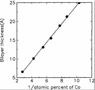
In order to test the correctness of the model and the equation, two groups (VIII and IX) of Co/Pd samples were made, and nominal and measured parameters concerning these sample structures are listed in Tables 3 and 4. One common point for these samples is that the nominal Co layer thickness is constant, and that deposition conditions such as sputtering pressure and sputtering power are the same for all samples. Therefore, it is expected that all samples within each group have the same interfacial structure. This means that if λ vs. 1/x (Co) is plotted, a straight line is expected. For samples listed in Tables 3 or 4, a line is indeed obtained, as shown in Figures 12 and 13. For the line in Figure 12 where λ vs. 1/x (Co) of samples in Table 3 is plotted, the intercept and slope can be easily calculated and their values are -0.134Å and 2.45Å for the intercept and slope, respectively. Because there are three unknown parameters: λa, x(Co)a, and na/nb, and only two equations, these three unknowns still cannot be uniquely determined. Therefore, other measurements to independently determine one of the three unknowns is required, as presented below.
The validity of the above equation can be verified by assuming a special case where the local composition x(Co)a is 1. That means that there is no interdiffusion between Co and Pd sublayers. Then, the nominal values of Co and Pd sublayer thickness should be recovered. It is found that in the case of x(Co)a=1, λa is 2.11Å, very close to the nominal value of 2Å. The nominal value of 4Å Co layers for Co/Pd samples in Table 4 is also recovered when the special case of x(Co)a=1 is assumed.
§4. Magnetic Measurements
Magnetic measurements were made on samples listed in Table 3. It turns out that the magnetic measurements are helpful to independently determine the interfacial layer thickness. The saturation magnetization σS of these samples are plotted vs. the nominal Pd layer thickness in Figure 14. Because of the induced moments on Pd atoms near Co atoms, the σS initially increases. It means that some of the 12 nearest neighbors of Pd atoms are Co atoms. When the Pd layer thickness increases, σS increases, indicating that the added Pd atoms still have some Co atoms as neighbors. σS keeps increasing until the Pd layer thickness reaches a value of about 10Å, as
shown in Figure 14. Therefore, the Pd atoms added after the layer thickness reaches about 10Å make no contribution to the magnetization. This indicates that Co atoms do not diffuse farther than 5Å in either direction.
Figure 12. Bilayer thickness λ vs. inverse of over-all Co composition of samples listed in Table 3.
Figure 13. Bilayer thickness λ vs. inverse of over-all Co composition of samples listed in Table 4.
Figure 14. Saturation magnetization σS vs. nominal Pd
From this experiment, it can be estimated that the Co-Pd mixing layer is about 12Å thick. Based on this estimation, the other two parameters in the above equation can be calculated: x(Co)a=20 at. % Co, and na/nb=1.026.
Some comments should be made about the above analysis. First, the local composition x(Co)a is the average value for sublayer a. Second, the atomic number ratio na/nb is very close to 1 but greater than 1, indicating that the average size of atoms in the a layers is slightly smaller than those in the b layers which is the case for Co/Pd multilayers. Finally, we point out that there is no crystalline structure information involved in the model, therefore the model should be equally applicable to amorphous multilayers. This model is applicable to multilayers with one very thin sublayer.
Summary
Multilayers consisting of ultra-thin sublayer were studied. It has been found that for sputter deposited multilayers, the chemical modulation along the perpendicular direction to the surface does not affect the diffraction line positions at large angle. Because of interdiffusion and alloying effects at interfaces, the lattice structure of the entire film tends to take the same form. The chemical modulation remains as the result of the deposition procedure. A simple model has been introduced to relate microstructural parameters such as interfacial layer thickness and local composition to
measurable quantities such bilayer thickness and over-all composition.
References
1. Gibson J.M., Osbourn G.C., and Tromp R.M. Materials Research Society Symposia. 56 (2001).
2. Falicov L.M., Pierce D.T., et al.J. Mater. Res., 5: 1299 (1998).
3. Sato N. J. Appl. Phys., 64: 6424 (1988).
4. Ochiai Y., Hashimoto S., and Aso K. lEEE-Tran. Mag.,
25: 3755 (2001).
5. Carcia P.F., Shah S.I., and Zeper W.B. Appl. Phys. Lett.,
56: 2345 (1990).
6. He P., McGahan W.A., Woollam J.A., Sequeda F.,
McDaniel T., and Do H. J. Appl.Phys., 69: 4021 (1991). 7. He P., McGahan W.A., Nafis S., Woollam J.A., Liou
S.H., Shan S.Z., Sequeda F., McDaniel T., and Do H.
Ibid., 70: 6044 (1991).
8. Fullerton E.E., Schuller I.K., Vanderstraeten H., and Bruynseraede Y. Phys. Rev. B., 112: 3056 (1999). 9. Clemens B.M. and Gay J.G. Ibid., 35: 9337 (1998). 10. Hollanders M.A. andThijsse B.J. J. Appl. Phys., 70: 1270
(1991).
11. Cullity B.D. Elements of X-Ray Diffraction. Addison-Wesley Publishing Co. (1978).
12. Bowen D.K. and Matyi R. XRD Workshop of 41st
Denver X-Ray Conference. Colorado Springs, Co.,
August 3-7, (1998).
13. Garaces Y. and Sanchez H. Thin Solid Films. 355: 487 (1999).
14. Ohring M. The Materials Science of Thin Films.
![Table 1. The general structure is [CoαPt1-α(βÅ)Pd(γÅ)]xτ. The parameters in parentheses indicate the variable parameters](https://thumb-us.123doks.com/thumbv2/123dok_us/192520.2013302/3.595.310.539.156.303/general-structure-coapt-parameters-parentheses-indicate-variable-parameters.webp)