Vertically aligned graphene based non-cryogenic
bolometer
Kiran Shankar Hazra1,3*, N. Sion2, Anil Yadav1, James McLauhglin2 and Devi Shanker Misra1
1
Department of Physic, Indian Institute of Technology Bombay, Mumbai-400 076 (India) 2
Nanotechnology and Integrated BioEngineering Centre, University of Ulster, Jordanstown, Newtownabbey, Northern Ireland, BT37 0QB (UK)
3
Physics & Astronomy Department, University of California, Los Angeles, CA-90025 (USA)
Abstract
*Corresponding author: Dr. K. S Hazra
In this paper we have thoroughly investigated the IR photoresponse of Vertically Aligned Graphene (VAG) at normal room temperature and have reported enhanced IR photo-response as compared the reports on CNTs. Graphene has already been proven to be very promising nanomaterial for applications in nanoelectronics, nanofillars etc. like its ancestor, carbon nanotube [10-17], however its photoresponse character is yet not well established. Here we have reported a swift electrical switching behavior due to photoresponse of the graphene samples in pulsed IR irradiation. Our investigations indicate that the photo-response in our graphene samples arise solely due to bolometric effect and not due to excitons or interband transition photoconductivity. The advantage of graphene as compared to CNTs is their higher surface area and unique band structure. Using vertically aligned grapheme (VAG) sample we have shown considerably higher response to IR irradiation as compared to CNTs.
In figure 1(a) shows the scanning electron microscopy (SEM) images of as the grown graphene samples. It is evident that the samples are almost vertically aligned with the graphene platelets having curved structure intercalated randomly to each other and form a mesh like network. The sizes of the platelets are found varying from ~100 nm to ~2 µm. Platelet tip consist of 5-10 layers of graphene and the base of the platelets are quite thicker perhaps consisting of 10-20 layers. The Raman spectra shown in figure 1(b) confirm the graphene structure with a strong 2D peak at 2700 cm-1. The intensity ratio of G-band and D-band is ~4, implies a well-defined
crystalline structure of the VAGs.
Figure 1: (a) SEM images of the graphene sample, showing intercalated graphene flakes, entangled in vertical direction to the sample surface. (b) Raman spectra of the VAGs shows sharp G and 2D peaks, including a low intensity D peak.
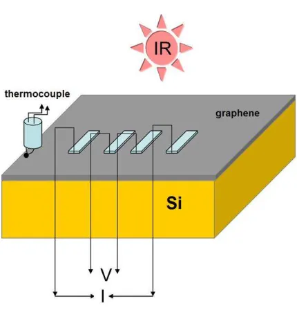
Figure 2. Schematic diagram of the experimental set up.
and not due to any change in contact resistance. The response time to reach the resistance from the baseline to saturation is ~ 5 sec. Such high response time and increase in resistance upon IR irradiation can occur only due to bolometric photo-response [8, 9, 18, 19]. Whereas for the photoresponses due to excitons or due to photoconductivity for interband transition, the response time would be much lower (ranges within 10-9 sec to 10-15 sec) and the resistance decreases upon IR irradiation. The normalized resistance R/R1 (R is the actual resistance and R1 is the maximum resistance during saturation) raised ~ 2 fold in the bolometric measurement at room temperature, which is quite remarkable. The sensitivity of the bolometer is defined as, ݏ =ோೞೌିோ್ೌೞ
ோ್ೌೞ
×
100%, where Rsat is the saturation resistance and Rbase is the base line resistance. In most of the
Figure 3: (a) I-V characteristics of VAGs at normal condition. (b) Electrical switching characteristics for pulsed IR irradiation.
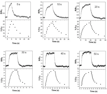
To investigate the behavior of the bolometric photoresponse of the VAG sample thoroughly we have recorded the resistance change for different pulse duration (5 s, 10 s, 20 s, 30 s, 40 s and 50 s) of IR irradiation. Figure 4 shows the changes in normalized resistance for different pulse durations and the corresponding temperature of the VAGs, measured by the thermocouple, which was directly in contact with the VAG flakes. For the 5 s pulse, the normalized resistance just reaches the saturation region, whereas for higher time duration pulses the saturation regions were well established. It was found from each plot that the normalized resistance varies with time (t) exponentially during heating and cooling as ோ
ோభ
= ݑ − ݒ expሺ−ݓ × ݐሻ and ோ
ோభ
= ܣ +
ܤ exp ሺ−ܥ × ݐሻ, respectively with u, v, w and A, B, C are positive constants. Also with higher
It is very clear from the figure that the resistance varies in similar fashion as the temperature reading of the thermocouple, confirming our argument to indentify the present photoresponse as bolometric. According to the thermocouple reading the steady state temperature is ~ (31 ± 1) 0C. The major difference between the temperature curve and the resistance curve is that the resistance curve approach towards the saturation much faster than the temperature curve, indicating higher response of the VAG bolometer than the thermocouple. To get a clear view of the temperature dependence of VAGs resistance we have plotted the hysteresis loop (figure 5) of normalized resistance w.r.t the thermocouple reading for 5 s IR pulse. Here the 5 s pulse was chosen to avoid the steady state saturation region and to get the response only during cooling and heating. At room temperature both the heating and cooling curve shows nonlinear response of resistance to temperature, although at low temperature and for short range temperature change the response may be considered as linear. During heating the normalized resistance rises rapidly with temperature at low temperature region and as the temperature increases the rate of increase becomes slower and approaches towards steady state; it follows the exponential function
ோ ோభ
= ߙ − ߚ expሺ−ߛ × ܶሻ , where α = 0.87, β= 322887, γ= 0.63 and T is the temperature in 0C.
The scenario reverses during cooling and it obeys the function ோ
ோభ= ݔ + ݕ expሺݖ × ܶሻ , where x
= 0.50, y = 8.9 x 10⁻¹² and z = 1.06. The change in resistance with temperature, ௗோ
ௗ் is positive for
heating curve and it shows negative value for cooling curve, which is expected for bolometric photo-response and it indicates metallic behavior of the VAGs. One of the important measuring parameter for bolometric response is the Thermal Coefficient of Resistance (TCR) and it is defined as, = ଵ
ோ ∆ோ
∆் , which is the normalized change in resistance with temperature. The TCR of
temperature rises from 18-23 0C, the TCR is ~11%/K, which is quite high TCR value as compared to previous reports of TCR on CNTs showing range within 0.01-3 %/K [1, 3, 4]. TCR can show higher values for lower temperature range as the temperature goes away from the steady state temperature and the slope of the heating curve increases. The reason for getting such high TCR in our case is probably the high surface area of the graphene as compared to CNTs. The flux of IR radiation will be much higher for graphene samples, especially for VAGs (due to their alignment), as compared to the CNTs. It could also be anticipated from previous reports[1, 3] that the TCR could be improved further at cryogenic temperature or arranging thermal isolation through vacuum for the VAG sample, which could pave a path towards next generation bolometric sensors.
In conclusion the VAG sample shows significant photoresponse as compared to CNTs. The electrical conductivity switching of I-V characteristics has been noticed upon pulsed irradiation of IR. Two fold increases in resistance was noticed from baseline to saturation region, which is due to bolometric effect. The resistance of the sample varies in a similar fashion as the temperature of the sample. The hysteresis of the VAG’s resistance shows TCR is ~11%/K for the temperature rising from 18 0C to 23 0C, which is the highest value, recorded for carbon nanomaterials. Also large surface area, catalyst free synthesis technique and strong adhesion to the substrate gives extra advantage to VAGs for bolometric applications.
Experimental:
Graphene preparation:
The synthesis of VAG samples was carried out in a SEKI Microwave Plasma Enhanced Chemical Vapour Deposition (MPECVD) deposition system. The system used a 1.5 kW, 2.45 GHz microwave power source. Heavily doped Si substrates were initially heated in-vacuum up to 900°C for the cleaning purpose and then subjected to nitrogen plasma at 650 Watts power and 40 Torr. The growth of VAGs was initiated by introducing CH4 into the chamber with a CH4/N2 gas flow in the ratio of 1:4. During the growth the microwave power was raised to 800 W and maintained during the growth time of 60 sec. The samples were then allowed to cool down under a constant N2 flow.
Instrumental:
References:
[1] M. E. Itkis, F. Borondics, A. Yu, R. C. Haddon, Science2006, 312, 413.
[2] B. Pradhan, K. Setyowati, H. Liu, D. H. Waldeck, J. Chen, Nano Lett2008, 8, 1142. [3] R. Lu, J. J. Shi, F. J. Baca, J. Z. Wu, J. App. Phy.2010, 108, 084305.
[4] F. Rao, X. Liu, T. Li, Y. Zhou, Y. Wang, Nanotechnology2009, 20, 055501.
[5] M. Freitag, Y. Martin, J. A. Misewich, R. Martel, P. Avouris, Nano Lett2003, 3, 1067. [6] M.E.Portnoi, O.V.Kibis, M. R. d. Costa, Proc. SPIE 2006, 6328, 632805.
[7] M. S. Dresselhaus, G. Dresselhaus, P. Avouris, Carbon nanotubes: synthesis, structure, properties, and applications, Vol. 80, Springer-Verlag, Berlin 2001.
[8] S. Maine, C. Koechlin, R. Fleurier, R. Haidar, N. Bardou, C. Dupuis, B. Attal-Trétout, P. Mérel, J. Deschamps, A. Loiseau, J.-L. Pelouard, Phy. St. Sol. C2010, 7, 2743.
[9] M. Tarasov, J. Svensson, L. Kuzmin, E. E. B. Campbell, App. Phy. Lett.2007, 90, 163503.
[10] A. A. Balandin, S. Ghosh, W. Bao, I. Calizo, D. Teweldebrhan, F. Miao, C. N. Lau, Nano Lett2008, 8, 902.
[11] M. A. Rafiee, J. Rafiee, Z. Wang, H. Song, Z.-Z. Yu, N. Koratkar, ACS Nano2009, 3, 3884. [12] K. S. Novoselov, A. K. Geim, S. V. Morozov, D. Jiang, M. I. Katsnelson, I. V. Grigorieva, S. V.Dubonos, A. A.Firsov, Nature2005, 438, 197.
[13] Y. Zhang, Y. W. Tan, H. L. Stormer, P. Kim, Nature 2005, 438, 201. [14] M. B. Lundeberg, J. A. Folk, Nat. Phy.2009, 5, 894.
[15] F. Miao, S. Wijeratne, Y. Zhang, U. C. Coskun, W. Bao, C. N. Lau, Science2007, 317, 1530. [16] H. B. Heersche, P. Jarillo-Herrero, J. B. Oostinga, L. M. K. Vandersypen, A. F.Morpurgo, Nature
2007, 446, 56.
[17] J. H. Chen, C. Jang, S. Xiao, M. Ishigami, M. S. Fuhrer, Nat. Nano.2008, 3, 206. [18] W. Xu, F. M. Peeters, T. C. Lu, Phy. Rev. B2009, 79, 073403.