Effect of Thickness on Properties of Copper Thin Films
Growth on Glass by DC Planar Magnetron Sputtering
A. Hojabri a, F. Hajakbari a, M. A. Moghri Moazzen b,*, S. Kadkhodaei a
a Department of Physics, Karaj Branch, Islamic Azad University, Karaj, Iran
bYoung Researchers Club, Karaj Branch, Islamic Azad University, Karaj, Iran
Abstract
Copper thin films with nano-scale structure have numerous applications in modern technology. In this work, Cu thin films with different thicknesses from 50–220 nm have been deposited on glass substrate by DC magnetron sputtering technique at room temperature in pure Ar gas. The sputtering time was considered in 4, 8, 12 and 16 min, respectively. The thickness effect on the structural, morphological and electrical properties were studied by X-ray diffraction (XRD), atomic force microscope (AFM) and four point probe (FPP) measurements, respectively. The results show that by increasing thickness, the copper films crystallinity in (111) direction increases. Also by varying the films thickness the significant changes were observed in the films surface morphology due to the mechanism of films growth. Finally, the relationship between film resistivity and Cu film thickness are investigated in this paper.
2012 JNS All rights reserved Article history:
Received 26/3/2012 Accepted 22/5/2012 Published online 1/6/2012
Keywords: Copper Thin film Nanoscale Thickness Morphology Resistivity
*Corresponding author: E-mail address:
m_moghri_moazzen@yahoo.com
Phone: 09119095028
Fax:
1. Introduction
In recent years, variety of practical and industrial applications of thin films is considered the importance of technological developments of thin films. Nowadays scientists and researchers are focused on film formation processes in order to obtain the insight into mechanisms leading to
special structural properties. Many parameters can influence on the thin films structure such as time, Ar gas pressure, kind of substrate and also the thickness, which determines the physical properties of the thin films.
and high electrical conductivity [1, 2]. Due to these characteristics; Cu thin films are widely used for many applications alike diodes [3], solar cells [4] and high-speed integrated circuits (IC) [5, 6]. The Cu thin films usually fabricated by different technique, including Reactive Pulsed Laser Deposition (RPLD) [7], DC magnetron sputtering [8], RF magnetron sputtering [9], ion beam assisted DC magnetron reactive sputtering [10] and molecular beam epitaxy (MBE) [11]. We choose the DC magnetron sputtering method because it has many advantages, such as high growth rate, the possibility of large area deposition, and low cost [12].
A lot of papers have been reported on the Cu thin film; however, most of them were using si substrates to deposit the films, while few reports treated the glass substrates [13]. In this study, the copper thin films have been prepared on glass substrates by DC planar magnetron sputtering at different time depositions. Then by using X-ray diffraction (XRD) (Philips pw 3710) analyses in the θ/2θ mode using Cu Kα X-rays, atomic force microscopy (AFM) and conventional four-point-probe (FPP5000) resistivity measurements, investigated the microstructural, surface morphology and electrical properties of Cu films. The effect of thickness on the structure and resistivity of the film will be briefly discussed.
2. Experimental procedure
In this work, Cu thin films with different thicknesses have been deposited on glass substrate by DC magnetron sputtering technique. The substrate was fixed directly above the Cu target (99.9% in purity) of 870mm in diameter with a target-to-substrate distance of 7 cm. The sputtering deposition was carried out in a pure argon (Ar) gas (99.999%) at a pressure from 6×10⁻⁵ to 8×10⁻² torr
and the sputtering power at 30 W which led to a deposition rate of approximately 12.5 nm/min. The size of glass substrates are 2 cm×3.5 cm and were cleaned ultrasonically in acetone and alcohol each for 15 min and blown dry in N2 gas before they
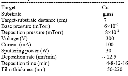
were introduced into the chamber. To illustrate the effect of the thin film thickness, four copper thin film samples with thicknesses at around 50–220 nm were prepared at room temperature. Film thickness was controlled by a quartz crystal mass monitor in the chamber. The deposition conditions of the Cu thin films are showed in Table 1.
Table 1. Deposition condition for the Cu thin films.
--- Target Cu Substrate glass Target-substrate distance (cm) 7
Base pressure (mTorr) 6×10⁻⁵
Deposition pressure (mTorr) 8×10⁻²
Voltage (V) 300 Current (mA) 100 Sputtering power (W) 30 Deposition rate (nm/min) ~ 12.5 Deposition time (min) 4-8-12-16
Film thickness (nm) 50-220
---
3. Results and discussion
(FCC) crystal structure and for this structure (111) face has the lowest surface energy [14].
When the thickness of samples is increased the crystallinity and the mean grain size improved. The average grain size of the films is estimated by scherrer formula [15], given by (Eq.1).The results are presented in Table 2.
D = 0.9λ/β cosθ (1)
4 6 8 10 12 14 16
40 60 80 100 120 140 160 180 200 220 240
F
ilm
t
h
ic
kn
es
s (
n
m
)
Deposition time (min)
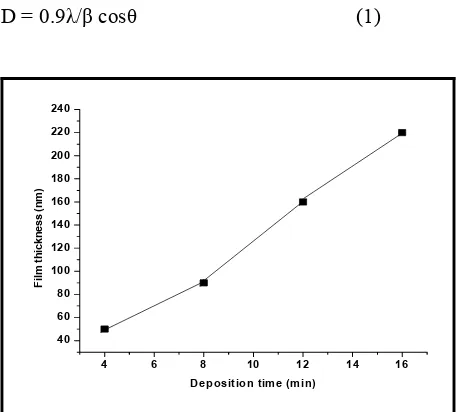
Fig. 1. Copper thin film thickness as a function of deposition time.
Table 2. Mean grain size of Cu thin films deposited on glass substrate.
Sample Time
(min) Thickness (nm) Grain Size (nm)
a 4 50 89
b 8 90 120
c
d
12 16
160 220
184 259
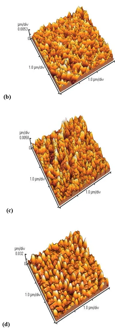
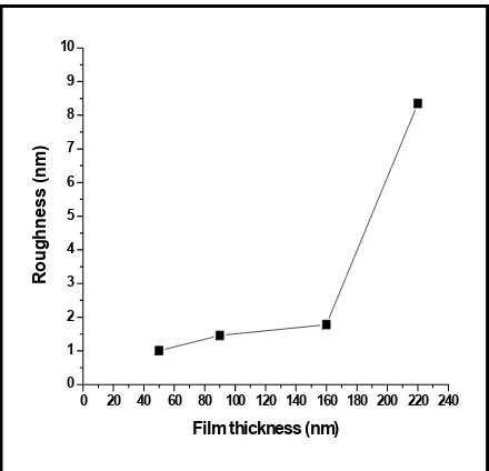
Three-dimensional surface morphology of thin films prepared in different thickness is shown in Figs. 3(a-d). AFM (1 µm×1 µm) examination of the Cu samples illustrated clearly that their surface morphologies are strongly affected by thickness. Figure (4) show that the grain size of the films clearly increase as the thickness rises, which is consistent with the XRD results. Investigation of the AFM images revealed that at the beginning of growth, the grain sizes are small (Fig. 3a) and Columnar structures for thin film were observed, which were tiny, dense, and vertical. By increasing thickness, these small grains gradually combine and make bigger grains (Figs. 3b, 3c). Finally, with increasing the thickness to 220 nm, the grains become bigger and at last it can cause to create clusters, which these clusters combine and create big grains which are shown in Fig. 3d. Also surface roughness of Cu films has been studied by AFM. As can be seen from Figure (5) when the film thickness increases from 50 to 220 nm, surface roughness increases from 1.001 to 8.353 nm, which results from an increase of grain size from 89 to 259 nm. It can be considered that the surface roughness of film originates significant from the surface morphology of the glass substrate.
(a)
(b)
(c)
(d)
40 60 80 100 120 140 160 180 200 220 240 80
100 120 140 160 180 200 220 240 260 280
G
rain siz
e
(nm
)
Film thickness (nm)
Fig. 4. Grain size of the Cu thin films deposited in different thickness.
0 20 40 60 80 100 120 140 160 180 200 220 240 0
1 2 3 4 5 6 7 8 9 10
R
o
ugh
ness (
n
m
)
Film thickness (nm)
Fig. 5. Dependence of the RMS roughness on the film thickness.
The electrical properties of Cu thin films with different thicknesses from 50 to 220 nm were investigated. Fig. 6 shows the dependence of the Cu film resistivity on thickness. The Cu thin film with 50 nm thickness has the highest resistivity value of 13.7 µΩ-cm and the
resistivity for thicker film of 90 nm is reduced to 5.51 µΩ -cm. The Cu thin film resistivity further decreases to 3.83 µΩ -cm as the film thickness increases to 160 nm, after which the resistivity is almost independent of the film thickness and the value varies at approximately 3 µΩ-cm. The lowest resistivity value is 2.2 µΩ-cm, obtained for Cu film with thickness 220 nm, which is the thickest film under investigation in the present work. The resistivity of thin films (ρ) can be expressed as [11]
ρ = ρp + ρm + ρf +ρi + ρs (2)
40 60 80 100 120 140 160 180 200 220 240 2
4 6 8 10 12 14
R
esisti
vi
ty
(
-cm
)
Film thickness (nm)
Fig. 6. Dependence of the electrical resistivity on the Cu film thickness.
4. Conclusion
We have investigated the thickness dependence of the structural and electrical properties of Cu thin films deposited on glass by dc planar magnetron sputtering method. The surface morphological study with AFM generally shows the enhanced nanostructure, while the XRD patterns reveal the improve crystalline quality for the thicker films. The RMS roughness was found to increase with increasing film thickness, which is associated with the increase in the crystal size due to surface energy minimization when the film gets thicker. The Cu film resistivity decreases with increasing film thickness to 220 nm, in which the decreasing trend can be attributed to the inverse linear dependence of film resistivity increase on crystal size. For the Cu films with160 nm thickness and larger, the thickness has no significant effects on the electrical properties, although the crystal size in these Cu films was observed to constantly increase. The phenomenon is attributed to exclusion of grain boundary scattering in limiting the electrical transport of the electrons in the relatively thick film having sufficiently large grains.
Acknowledgment
The financial support of this work by Islamic Azad university of Karaj Branch.
References
[1] T. Nitta, T. Ohmi, M. Otsuki, T. Takewaki, T. Shibata. J Electrochem Soc 1992;139:922.
[2] T. Kikkawa, T. Oyobutsuri. Jpn J Appl Phys 1999; 68:1215.
[3] H. Nienhaus, H. S. Bergh, B. Gergen, A. Majumdar, W. H. Weinberg, and E. W. McFarland Ultrathin Cu films on Si(111): Schottky barrier formation and sensor applications, J. Vac. Sci. Technol. A 17, 1683 (1999)
[4] Cu(InGa)Se2 Thin-Film solar cells: comparative
life-cycle analysis of buffer layers, 22nd European Photovoltaic Solar Energy Conference, Milan, 3-7 September 2007.
[5] Kim K J, Kim J H and Kang J H 2001
J.Cryst.Growth 222767
[6] T. S. Cale, T. P. Merchant, L. J. Borucki, and A. H. Labun, Thin Solid Films 365, p.p152 2000.
[7] Wasa K, Kitabatake M, Adachi H. Thin film materials technology: sputtering of compound materials. New York: William Andrew Inc; 2004. [8] Y. Mikami, K. Yamada, A. Ohnari, T. Degawa, T. Migita, T. Tanaka, K. Kawabata, H. Kajioka, Surface and Coatings Technology 133–134 (2000) 295. [9] J. F. Pierson, Vacuum, 66 (2002) 59.
[10] I. M. Odeh, J. Alloy and Compound 454 (2008)102.
[11] Robin F.C. Molecular beam epitaxy: applications to key materials; Newyork: William Andrew Inc; 1995.
[12] Kah-Yoong Chan, Teck-Yong Tou, Bee-San Teo, Microelectronics Journal 37 (2006) 608–612. [13] Hong Qiu, Fengping Wanga, Ping Wua, Liqing Pana, Yue Tiana, Vacuum 66 (2002) 447–452
[14] N. Joshi, A.K. Debnath, D.K. Aswal, K.P. Muthe, M. Senthil Kumar, S.K. Gupta, J.V. Yakhmi, Vacuum, 79 (2005).
[15] West AR (1991) Solid state chemistry and its application. Wiley, Newyork, pp 174-175.
[16] N. Paik, Nuclear Instruments and Methods in Physics Research B 229 (2005) 438.