Structural and compositional changes in single wall carbon nanotube
ensemble upon exposure to microwave plasma
SoumyenduRoy,1,a)ReetiBajpai,2NavneetSoin,3SusantaSinha Roy,4
James A.McLaughlin,5and D. S.Misra6,b)
1
Advanced Technology Development Centre, Indian Institute of Technology Kharagpur, Kharagpur 721302, India
2
Department of Chemistry and Thematic Unit of Excellence, Indian Institute of Technology Kanpur, Kanpur 208016, India
3
Institute of Renewable Energy and Environment Technology, Institute for Materials Research and Innovation, University of Bolton, Deane Road, Bolton BL3 5AB, United Kingdom
4
Department of Physics, School of Natural Sciences, Shiv Nadar University, Chithera, Uttar Pradesh 203207, India 5
Nanotechnology and Integrated Bioengineering Centre, University of Ulster at Jordanstown, Newtownabbey BT37 0QB, Northern Ireland, United Kingdom
6
Department of Physics, Indian Institute of Technology Bombay, Mumbai 400076, India
(Received 11 June 2017; accepted 4 October 2017; published online 18 October 2017)
Microwave plasma treatment of single wall carbon nanotube (SWNT) films called bucky papers (BPs) resulted in changes in the relative proportion of different chiralities of SWNTs present in the BP and the production of vertical microstructures on the surface of BP. The plasma was created using H2gas mixed with Ar or CH4, at a temperature of 900C and a pressure of 70 Torr. Radial breathing mode spectra of the BPs revealed that the preferential sputtering by plasma is not with respect to the diameter or the metallic nature of SWNTs. We propose that the lengths of SWNTs influence how they interact with plasma. Longer tubes will have higher dielectric constants and hence will be polarized more strongly by the electric field of the plasma sheath. This in turn results in greater ion bombardment and sputtering. Finite element method was used to find the strengths of the induced electric fields on model SWNT surfaces. Microscopy, Raman, and X-ray photoelectron spectroscopy were used to study the effect of plasma on the crystallinity of the surviving SWNTs. Structural integrity of SWNTs was preserved after the plasma treatment. Published by AIP Publishing.https://doi.org/10.1063/1.4989658
INTRODUCTION
Low temperature plasma is a versatile tool for fabrica-tion and modificafabrica-tion of nano-materials, thin films, and semi-conductors.1,2 Consisting of charged particles and excited neutrals, plasma provides a unique environment for chemical reactions, which is distinct from what one can achieve with ordinary solid, liquid, and gas phases. It has been used for synthesis, surface functionalization, doping, and purification of carbon nanotubes (CNTs) and to modify morphology of CNT based structures at the nano and microscales.3–11 We had previously demonstrated that plasma treatment can con-vert the surface of a free standing single wall CNT (SWNT) film [otherwise known as bucky papers (BPs)] consisting of densely packed horizontal SWNTs into an array of vertical microstructures having shapes that resemble cones and pil-lars.12BP retains its flexibility after plasma modification and can be integrated with any device. Mixtures of H2þAr and H2þCH4gases were used for the treatment. This lithography free technique of making vertically aligned CNT microstruc-tures was instrumental in improving the performance of devices like field emitters, supercapacitors, and dye sensi-tized solar cells that were fabricated using the BPs.12,13
Here, we discuss the effect of the plasma treatment on the chiral make-up of the SWNTs in BPs. There have been very few studies on the effect of plasma on the composition of SWNTs.14–16The results presented here is in sharp contrast to the previously reported preferential etching of metallic SWNTs over the semiconducting ones. No differential etching on the basis of diameter or conducting nature was observed in our experiments. However, some tubes appeared to be sputtered or etched much faster than others. The temperature of plasma is a vital difference between ours and the previous studies. We explore the possibility of a variation in length of as synthesized SWNTs being a determining factor in the differential effect of plasma. We show that there can be significant variation in the strength of the electric field at the surface of tubes with differ-ent lengths, placed inside a plasma environmdiffer-ent. It was also noticed that the crystallinity of the nanotubes that survived the plasma treatment did not deteriorate but rather showed a mod-erate improvement. These effects were studied by Raman and X-ray photo-electron spectroscopy (XPS).
EXPERIMENTAL SECTION
SWNT and BP synthesis
SWNTs were grown by catalytic chemical vapor deposi-tion (CVD) method. CH4 diluted with H2 gas (1:5 by vol-ume) was blown over the heated catalyst kept at a a)
Author to whom correspondence should be addressed: anoyonline@gmail. com. Phone:þ918942857481.
b)Current address: IIa Technologies Pte Ltd., Singapore 618300.
temperature of 960–970C and under atmospheric pressure. The catalyst used is a solid solution of the bimetals Co-Mo or Fe-Mo in MgO (Co:Mo:MgO¼1:0.5:300 and Fe:Mo:MgO¼1:0.5:200 by weight) prepared by combustion synthesis technique. Most of the SWNTs were estimated to have diameters lying between 1.13 and 1.65 nm.17 The experiments reported here were generally carried out using the SWNTs made from Co based catalyst. However, there was no discernable difference with the Fe catalyst grown SWNTs. After synthesis the catalyst material was separated from the tubes by dissolution in 11 M HNO3 solution. Purified SWNTs were dispersed and filtered through a poly-vinylidene fluoride membrane under an applied pressure gra-dient.18 After drying the SWNT BPs are separated from the filter by dipping in N,N-dimethyl acetamide. BPs used in these experiments were robust, flexible, 1.7–1.8 cm in diameter, and 10–12lm in thickness.
Plasma treatment of BP
Plasma treatment was performed inside a microwave plasma CVD chamber (2.45 GHz frequency) with magnetron operated at 400 W power, temperature of 900C, and pressure of70 Torr. The base pressure of the chamber was approximately 102Torr, and the gas mixtures used to create the plasma were H2þAr and H2þCH4 with approximately 98% H2by volume in both cases. The substrate temperature was measured using an IRCON make Optical Pyrometer. H2 gas on its own was found to produce minor changes under identical conditions; therefore, heavier gases had to be mixed. N2plasma was avoided because it is known to dope CNTs.8
Raman spectroscopy
Horiba Jobin Yvon HR 800 confocal micro-Raman spectrometer equipped with an Argon ion laser of wave-length 514.5 nm (2.41 eV), ISA LabRam system equipped with a 632.8 nm (1.96 eV) He–Ne laser, and an Avalon Raman Station-CT system with a 785 nm (1.58 eV) laser was used to record the Raman spectra. Typical resolutions were better than 0.5 cm1, 2 cm1, and 4 cm1, respectively. The signals were recorded in back scattering geometry, at room temperature with laser powers below 5 mW. The three dif-ferent laser energies used cover almost the entire diameter range of SWNTs up to 3 nm. The low frequency radial breathing mode (RBM) spectra of the SWNTs were analyzed in order to identify their diameters and chiralities. A detailed description of the process can be found in our previous publi-cation17 and it is similar to what has been reported by others.19–23 Briefly, the spectra were fitted with Lorentzian peaks having full width at half maxima (FWHM) of 16 cm1.20,21 Spectra obtained at 6–9 different spots were normalized, and an average of these was used for fitting. From the RBM peak frequencies (xin cm1), the diameters (din nm) of the SWNTs were calculated using the relation x¼234/dþ10.21,22 Exploiting the resonant nature of the Raman scattering from SWNTs further information regard-ing its atomic structure can be obtained from the RBMs. By comparing the values of laser energy and diameters of the
corresponding resonant SWNTs with the coordinates of a Kataura plot, the most probable chiralities (n,m) of the tubes can be estimated. The Kataura plot was calculated using tight binding approximation for nearest neighbor interactions with carbon-carbon interaction energy of 2.9 eV.19,21,24 Full details have been reported elsewhere.17Tubes with (n – m) equal to an integral multiple of 3 were considered metallic.
Other characterizations
The microscopic observations of the SWNTs were car-ried out in a high resolution transmission electron micro-scope (TEM, model: JEOL, JEM 2100F). The BPs after exposure to plasma were dispersed in isopropanol by ultra-sonication for TEM. Surface topography of the BPs was investigated using a scanning electron microscope (SEM, model: Jeol, JSM6400). X-ray photoelectron spectroscopy (XPS) measurements used in this study were conducted in Thermo VG Scientific Multilab 2000 system with elec-tron energy analyzer model CLAM4. The resolution of the instrument was 0.75 eV. The Al-Ka radiation (h ¼1486.6 eV) lines were used for measurements, and the pressure was 41010Torr.
Electric field simulation
The static electric field at the surface of the CNTs was visu-alized by using finite element analysis. Comsol Multiphysics version 3.3 was used for solving the Laplace’s equation in the presence of dielectric media:r: e0rVP~
¼0, wheree0is
the permittivity of free space,Vis the electric potential, andP~is the polarization vector. The purpose of the simulation was to get an approximate idea of how the electric field at the CNT surface changes as its length and dielectric constant change. Hence, the model used was kept very simple. It consisted of a cube of edge 20lm and a nanotube of diameter 5 nm placed at its center (Fig. S3 of thesupplementary material). The length of the nanotube was set at 5, 1, and 0.1lm for the different simulations. Lower tube diameter or higher aspect ratios could not be achieved because of the constraints in computing resources. The simula-tions were performed in 3D mode using the electrostatic mod-ule. z¼10lm wall of the cube was set at 40 V potential, the wall at z¼-10lm was grounded and the rest were set symmet-ric. These boundary settings produced a uniform field inside the cube equal to that of the plasma sheath, in the absence of any perturbation due to the nanotube. The solid nanotube subdomain had dielectric constants calculated later in the text, while the rest of the space had dielectric constant of 1. The mesh consisted of 2.8105tetrahedral elements, with higher density around the nanotube. Further refinement in meshing did not produce any significant changes in the electric field distribution at the tube.
Results and discussions
A complex interplay between different factors like the plasma sheath potential, polarization of the SWNTs, inter tubular cohesive forces, and ion bombardment can result in the for-mation of these microstructures on the BP surface. These changes have been discussed in our previous publication.12 Spatial variations in plasma properties, both along the plane of the BP surface and perpendicular to it, may also give rise to anisotropic etching, producing microstructures of different shapes. Similar patterns produced on Si and other materials have been observed previously.25
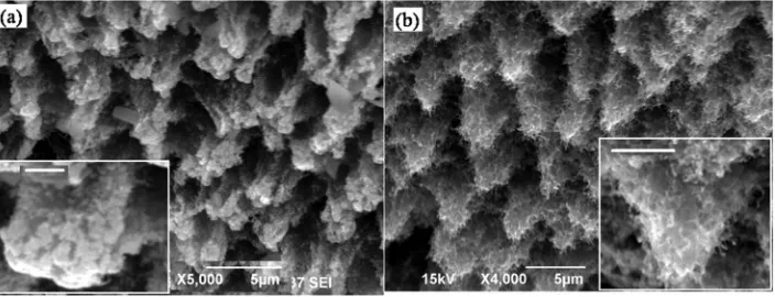
Another conspicuous difference between the effects of Ar and CH4based plasmas is the tube-like structures emanat-ing from the cones in CH4plasma treated BPs [see inset of Fig.1(b)]. No such features can be seen in the pillars of Ar plasma treated BPs. These features turned out to be multi-wall CNTs (MWNTs) as shown in Fig. S2 of the
supplemen-tary material. These MWNTs grew on the surface of BP
during the treatment. The CH4 in the plasma provides a source of carbon, left over impurities with Fe or Co based nanoparticles enclosed inside graphitic shells provide the necessary catalytic effect, and the high temperatures (900C) of the plasma provide a suitable ambient for the growth of these MWNTs. Apart from these, the etching rates of the two types of plasmas were also different.
Raman spectroscopy revealed that although plasma treatment etches the BP, it does not result in creation of defects in the lattice structure of SWNTs. The ratio of the intensities of the D band (ID, at 1350 cm1) to the G band (IG, at1580 cm1) provides a measure of the defects in the sp2structure of the nanotube walls.19,21As shown in the inset of Fig.2(a), the ID/IGratio drops as a result of the treatment. From an initial value of 0.1 in the pristine BP, it becomes
0.067 after 4 h. of CH4 þH2 plasma irradiation and 0.045 after 2 h. of ArþH2plasma irradiation. This is counterintui-tive to what one would normally expect from an etching pro-cess. It is possible that the plasma instead of etching individual SWNTs is sputtering whole nanotubes away from the BP. Thus, the BP appears to be getting etched while the SWNTs that survive in the BP have their atomic structure undamaged. TEM imaging of the plasma treated SWNTs also confirm that the crystallinity of the nanotubes remained intact after the treatment as can be seen from Fig.2(b).
Inset is a TEM micrograph of SWNTs obtained from the BPs treated with Ar plasma, showing the undamaged walls of individual nanotubes. The scale bar is 10 nm.
Sputtering of whole SWNTs can explain the lack of increase in ID/IGratio, but cannot explain the decrease in this ratio. One possible explanation is that the plasma is knocking out the oxygen containing functional groups that were cova-lently bonded to the SWNT walls. These groups, mainly the hydroxyl group, are formed during the purification and BP formation step using HNO3, which is an oxidizing agent.26,27 This conjecture is corroborated by data from XPS. Figure
2(b) shows the XPS spectra before and after plasma treat-ment. The peak at 284.5 eV originates from sp2hybridized carbon atoms that make up the walls of the nanotubes. The hump at 286 eV is a characteristic of the COH bonds,26 and we found that it decreased in intensity after both Ar and CH4 plasma treatments. The carbon-oxygen weight ratio in pristine BP obtained from the ratio of the areas under the C1s and O1s peaks in the XPS spectrum is about 75%:25%. The exposure to ArþH2 plasma for 2 h and CH4 þH2 plasma for 4 h reduces the oxygen content to approximately 19% and 16%, respectively. It is also interesting to note that FIG. 1. Changes in the morphology of BP surface after plasma treatment. (a) Pillar type microstructures with blunt tips formed after 2 h. of ArþH2plasma treatment. (b) CH4þH2plasma etches the top of BP more rapidly than the bot-tom, resulting in cone type structures with sharper tips. Scale bars of the mag-nified insets are (a) 1lm and (b) 2lm.
although the oxygen removal is higher in the case of CH4 plasma etching, the decrease in ID/IG ratio is much smaller. A possible reason behind this is the formation of the defec-tive MWNTs on the surface of BP after CH4plasma etching. Since the MWNTs cover the surface, a significant fraction of the Raman signal probably comes from them. XPS spectra also show the absence of any doping or functionalization of the nanotubes due to the treatment. It is also possible that annealing at high temperatures results in atomic rearrange-ments and defect healing in the SWNTs28causing a reduc-tion in the ID/IGratio.
It was observed that microwave plasma has different rates of sputtering for nanotubes with different chiralities resulting in changes in the composition of BP after the treat-ment. As shown in Fig. 3, certain RBM peaks disappear from the Raman spectrum while some others survive. From the graphs, it is also clear that the results of both CH4þH2 and ArþH2 plasma irradiation for 4 and 2 h, respectively, are almost identical. The use of three different lasers for Raman spectroscopy allows a more complete identification of the different tubes present in the sample. The RBM spec-tra were fitted with individual Lorentzian peaks and the diameters compared with a theoretical Kataura plot to iden-tify the chiralities. The method has been described in details in our previous publication.17By comparing the RBM spec-tra before and after plasma treatment, the tubes that were get-ting preferentially sputtered were identified and listed in TableI.
The progressive changes in the RBMs after different plasma irradiation durations are shown in Fig. 4. The changes in the RBMs occur very quickly. It can be seen in the figure that after just 30 min and 1 h of treatment with Ar
and CH4 based plasmas, the 188 cm1 peak in the RBM spectra obtained with 514.5 nm laser has diminished signifi-cantly. Longer plasma treatment durations, 3 h with Ar and 5 h with CH4mixtures, were also tested. But these only lead to more sputtering and weakening of the BP without any changes in the relative abundances of the different SWNTs.
A striking feature of the selective etching effect is that the selectivity is neither w.r.t. diameter nor the conducting nature of the tubes. Both small and large diameter tubes get etched. There does not seem to be any continuous variation with diameter. For example, in the 514.5 nm spectra [Figs.
3(a) and 3(d)], we can see that the two RBM peaks at 170 and 188 cm1(corresponding to 1.46 and 1.31 nm diameters) shrink as a result of the treatment, but the peaks just outside this range at approximately 155 and 210 cm1 (1.61 and 1.17 nm diameters) suffer relatively much less damage. Similarly both metallic and semiconducting tubes are removed by the plasma as is evident from Table I. In 514.5 nm spectra, both the disappearing tubes are semicon-ducting ones while in the 632.8 nm spectra only metallic tubes are removed. The 785 nm spectra indicate that a com-bination of both metallic and semiconducting SWNTs is get-ting sputtered.
through simple microwave irradiation in an oven29–31or pho-tolysis in air by irradiation with laser of appropriate wave-length32 is also known to destroy metallic SWNTs preferentially. As mentioned before, no such differential etching on the basis of radius and conducting nature was observed in our case. The mechanism behind preferential etching is the differential bombardment of the tubes by ions present within the plasma. Apart from the metallic nature and diameter, other parameters like length can also give rise to selective sputtering of the tubes as explained below.
The plasma will create a positively charged region called the sheath, around the BP surface. This is due to the different thermal energies of the ions and electrons in the plasma. The spatial extent of the sheath is of the order of the Debye length (k), which for a particular species in the plasma is given byk2¼0kT
nq2, where0is the permittivity of
free space,kis the Boltzmann constant, n,q, andTare the density, charge, and temperature (in Kelvin) of the particular species under consideration.33The Debye length (in meters) for electrons turn out to bek¼7:4103
ffiffiffiffiffi TeV
n q
, whereTeVis
temperature of the electrons in eV. The self-potential of plasma or sheath potential is defined as /¼TeVln pffiffiffiffiffiffiffiffiffiffiffiffiffiffiffiffiffiffimi=4pme
, where mi and me are the rest
masses of the ions and electrons, respectively. In earlier
studies, characteristics of the plasma formed under similar con-ditions with a mixture of H2and CH4gases in our microwave plasma CVD system have been investigated.34 The tempera-ture and density of electrons were found to beTeV10 eV and n1012cm3¼1018m3. With these parameters, the Debye length turns out to be 20lm. If we assume that similar plasma conditions prevail with ArþH2 mixture as well, then the sheath potentials due to the CH4 and Ar ions turn out to be
39 and 43 V, respectively. Potential due to H2ions, which are more abundant, will be28 V. The value of the static elec-tric field across the sheath is approximately between 1.4 and 2 V/lm, depending on the relative concentration of the CH4 (or Ar) and H ions in the sheath. This field will exist in a direc-tion perpendicular to the BP surface.
The SWNTs will get polarized when placed in the exter-nal electric field (E) and behave as dipoles.35–38The compo-nents of the induced dipole moment (p) of the nanotube along and perpendicular to its length are given bypk¼lakEk
andp?¼la?E?, whereais the polarizability per unit length
(l). However,a?is orders of magnitude smaller38and can be
neglected here. Tight binding theory predicts an infinite ak
for metallic SWNTs. But using classical electrostatics and approximating the tube as a very small, solid metallic cylin-der placed in an uniform external field gives
ak¼ l
2
24 lnð ðl=RÞ1Þ 1þ
4=3ln2 lnðl=RÞ1
ð Þ
h i
, where R is the radius of the tube.37–39 The value of ak for semiconducting nanotubes
obtained using tight binding approximation is much lower at
ak¼17:8 R
3
a2 ccc20
, where acc is the carbon–carbon bond length (0.142 nm) andc0is the tight binding nearest neighbor
inter-action energy (2.9 eV).36,37However, the temperature of the plasma (900C) is high enough to excite a significant num-ber of electrons from the valence band of semiconducting tubes (whose band gap is low,0.6 eV for tubes of diameter 1.3 nm) to the conduction band. Thus, the difference between semiconducting and metallic tubes becomes blurred36 and the metallic cylinder approximation can be used for both types of tubes.
The ions are accelerated through the sheath potential to the BP surface which is at negative potential w.r.t. plasma. Locally on the BP surface, there will be different types of tubes which will be polarized to different extents and create different local fields around themselves. Some will attract more ions as compared to others. Since the perpendicular component of polarizability is much lower than the parallel TABLE I. Diameters and chiralities of the nanotubes that are etched most
rapidly during the plasma treatment (*¼metallic SWNT). A few extremely low intensity peaks in the original sample have not been considered here.
Laser wavelength (nm)
RBM peak position (cm1)
Diameter (nm)
Matching chiralities (n,m)
514.5 170.39 1.46 13,8
188.00 1.31 12,7 10,9, 14,4
632.8 188.49 1.31 16,1* 11,8*
195.71 1.26 12,6*
209.41 1.17 10,7*
217.84 1.13 11,5*
785 138.70 1.82 20,5* 18,8 16,10*
151.80 1.65 12,12*
161.00 1.55 19,1*
170.80 1.46 16,4* 12,9*
204.71 1.21 12,5
229.78 1.06 11,4
252.28 0.97 8,6 9,5
308.58 0.78 8,3
component we can drop the subscript kfor simplicity and assume the parallel components to be equal to the net values. Polarization or dipole moment per unit volume P¼aE/ A¼0vE, whereA is the area of cross-section of the
nano-tube,0is the permittivity of free space andvis the
suscepti-bility of the tube. Hence, the dielectric constant
r ¼1þv¼1þAa0.40 ais generally expressed in units of
(length),2for converting to SI units one has to multiply it by
4p0.Hence, the dielectric constant in SI units is 1þ4Ra2 and it depends both onlandR. For example, SWNTs with diam-eter of 1.35 nm and lengths 0.1, 1, and 5lm havervalues of
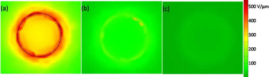
about 0.1104, 6.4104, and 124.9104, respectively. The induced electric field just outside the nanotube is depen-dent on the dielectric constant. There is no simple analytical relationship between the two. Hence, the fields were simu-lated using finite element method.
Figure 5shows the strength of the fields at the tips of SWNTs modeled as solid cylinders with the same diameter but different lengths, placed inside an external electrostatic field. The magnitude of the field at the edge of 5lm tube is
550 V/lm while the same at 100 nm tube is 25 V/lm. Hence, ions will be preferentially attracted towards the lon-ger tubes, causing more bombardment and sputtering. The increase in electric field strength at the SWNTs is expected from the increase in dielectric constant values. The simula-tion done in the current study was only meant to be an aid for visualizing this increase and not for reproducing the exact field distribution at the BP film (which consists of a random distribution of different types and spatial orientations of SWNTs) placed inside microwave plasma. Other phenomena like the complex electromagnetic interactions between the different charged species in plasma and the SWNTs or the microwave radiation and SWNTs will also affect the field distributions. Electrostatic screening effects due to adjacent tubes might further enhance the differential ion bombard-ment on the tubes. To account for all such processes, one would require more rigorous finite element simulation, which is beyond the scope of the current study.
It is important to note that the bombardment by ions accelerated through the plasma sheath plays a much more important role in sputtering of SWNTs than the bombard-ment due to the random motion of electrons. The energy of the ions due to their random thermal motion is of the order
of 5–10 eV.34,41 They gain an additional 28–40 eV as they accelerate through the sheath. Electrons have an average thermal energy of 10 eV. Only a fraction of the electrons that are highly energetic will be able to cross the potential barrier of the sheath and reach the tubes. On top of that their compo-nent of motion along the field will be slowed down by the sheath potential. Length dependent ion bombardment can explain why SWNTs with certain random diameters and chiralities disappear, while others survive the plasma. Longer length results in higherrand higher field at the
sur-face that ultimately leads to more ion impingement in plasma.
CONCLUSION
Irradiation of SWNT BP with microwave plasma resulted in the preferential removal of certain tubes from the BP over others. Because of the high temperature of plasma (900C) the selectivity was not w.r.t. metallic/semicon-ducting nature of the nanotubes. There was also no direct correlation with diameter of the tubes. We propose that the length variation of the SWNTs could be responsible for the observed preferential removal. Approximating the SWNTs as small metallic cylinders in an external electric field, we estimate the different dielectric constants for different lengths. The strength of the electrostatic field due to plasma sheath at the SWNTs was simulated using finite element method and was found to be much higher for longer tubes of same diameter. This would result in stronger ion bombard-ment and faster sputtering of the longer tubes from BP. ID/IG ratios in Raman spectra and TEM images suggest that the crystallinity of SWNTs is preserved after the treatment and XPS reveals a loss of -OH functional groups attached to the nanotubes. The treatment also created micron sized verti-cally aligned structures on the surface of BP. The shape of these microstructures could be changed from pillar-like to cone-like by changing the gas mixture used to create the plasma from ArþH2to CH4þH2.
SUPPLEMENTARY MATERIAL
See supplementary material for TEM images of
MWNTs and SWNTs, SEM images, photographs of BP, and
diagram of the model used for simulation. This material is available free of charge via the Internet.
ACKNOWLEDGMENTS
S.R. and R.B. acknowledge the financial support from DST, India, via the DST INSPIRE Faculty Award (Nos. DST/INSPIRE/04/2015/002287 and/04/2015/002318). The authors acknowledge the Centre for Research in Nanotechnology & Science (CRNTS), Central Surface Analytical Facility (ESCA), IRCC, IIT Bombay for the measurements. S.R. thanks United Kingdom – India Education and Research Initiative (UKIERI) for funding his work at the University of Ulster at Jordanstown.
1J. Zheng, R. Yang, L. Xie, J. Qu, Y. Liu, and X. Li,Adv. Mater.22, 1451 (2010).
2K. Ostrikov, Plasma Nanoscience: Basic Concepts and Applications of
Deterministic Nanofabrication (Wiley-VCH Verlag GmbH & Co. KGaA, Weinheim, 2008).
3
A. Kumar, S. Parveen, S. Husain, J. Ali, M. Zulfequar, Harsh, and M. Husain,J. Appl. Phys.115, 084308 (2014).
4
P. K. Tyagi, A. Misra, M. K. Singh, D. S. Misra, J. Ghatak, P. V. Satyam, and F. Le Normand,Appl. Phys. Lett.86, 253110 (2005).
5
K. S. Hazra, P. Rai, D. R. Mohapatra, N. Kulshrestha, R. Bajpai, S. Roy, and D. S. Misra,ACS Nano3, 2617 (2009).
6
I. Dumitrescu, N. R. Wilson, and J. V. Macpherson,J. Phys. Chem. C111, 12944 (2007).
7
S. Huang and L. Dai,J. Phys. Chem. B106, 3543 (2002). 8
N. Soin, S. Sinha Roy, S. Roy, K. S. Hazra, D. S. Misra, T. H. Lim, C. J. Hetherington, and J. A. McLaughlin,J. Phys. Chem. C115, 5366 (2011). 9
L. Bareket, N. Waiskopf, D. Rand, G. Lubin, M. David-Pur, J. Ben-Dov, S. Roy, C. Eleftheriou, E. Sernagor, O. Cheshnovsky, U. Banin, and Y. Hanein,Nano Lett.14, 6685 (2014).
10A. Davydova, E. Despiau-Pujo, G. Cunge, and D. B. Graves,J. Appl.
Phys.121, 133301 (2017).
11B. B. Wang, Q. J. Cheng, X. X. Zhong, Y. Q. Wang, Y. A. Chen, and K. Ostrikov,J. Appl. Phys.111, 044317 (2012).
12S. Roy, R. Bajpai, N. Soin, P. Bajpai, K. S. Hazra, N. Kulshrestha, S. S. Roy, J. A. McLaughlin, and D. S. Misra,Small7, 688 (2011).
13S. Roy, R. Bajpai, A. K. Jena, P. Kumar, N. kulshrestha, and D. S. Misra,
Energy Environ. Sci.5, 7001 (2012).
14G. Zhang, P. Qi, X. Wang, Y. Lu, X. Li, R. Tu, S. Bangsaruntip, D. Mann, L. Zhang, and H. Dai,Science314, 974 (2006).
15A. Hassanien, M. Tokumoto, P. Umek, D. Vrbanicˇ, M. Mozeticˇ, D. Mihailovic´, P. Venturini, and S. Pejovnik,Nanotechnology16, 278 (2005). 16
G. Zheng, Q. Li, K. Jiang, X. Zhang, J. Chen, Z. Ren, and S. Fan,Nano Lett.7, 1622 (2007).
17S. Roy, R. Bajpai, N. Soin, S. S. Roy, J. A. McLaughlin, and D. S. Misra,
Appl. Surf. Sci.321, 70 (2014). 18
S. Roy, V. Jain, R. Bajpai, P. Ghosh, A. S. Pente, B. P. Singh, and D. S. Misra,J. Phys. Chem. C116, 19025 (2012).
19M. S. Dresselhaus, G. Dresselhaus, R. Saito, and A. Jorio,Phys. Rep.409, 47 (2005).
20
Z. Yu and L. Brus,J. Phys. Chem. B105, 1123 (2001). 21
A. Jorio, M. Pimenta, A. Souza Filho, R. Saito, G. Dresselhaus, and M. Dresselhaus,New J. Phys.5, 139 (2003).
22M. S. Dresselhaus, G. Dresselhaus, A. Jorio, A. G. Souza Filho, and R. Saito,Carbon40, 2043 (2002).
23
A. Jorio, R. Saito, J. H. Hafner, C. M. Lieber, M. Hunter, T. McClure, G. Dresselhaus, and M. S. Dresselhaus,Phys. Rev. Lett.86, 1118 (2001). 24
S. Reich, C. Thomsen, and J. Maultzsch, Carbon Nanotubes: Basic Concepts and Physical Properties (John Wiley and Sons, Weinheim, 2008).
25L. Sainiemi, V. Jokinen, A. Shah, M. Shpak, S. Aura, P. Suvanto, and S. Franssila,Adv. Mater.23, 122 (2011).
26
C. Hontoria-Lucas, A. J. Lopez-Peinado, J. d. D. Lopez-Gonzalez, M. L. Rojas-Cervantes, and R. M. Martın-Aranda,Carbon33, 1585 (1995). 27G. Xu, Q. Zhang, W. Zhou, J. Huang, and F. Wei,Appl. Phys. A92, 531
(2008). 28
A. Ramos, I. Camean, and A. B. Garcıa,Carbon59, 2 (2013). 29
B. R. Priya and H. J. Byrne,J. Phys. Chem. C113, 7134 (2009).
30J. W. Song, H. W. Seo, J. K. Park, J. E. Kim, D. G. Choi, and C. S. Han,
Curr. Appl. Phys.8, 725 (2008). 31
L. Wang, Y. Xiong, Z. Wu, B. Duong, S. Seraphin, H. Xin, and L. Chen,
Appl. Phys. A102, 401 (2011).
32H. Huang, R. Maruyama, K. Noda, H. Kajiura, and K. Kadono,J. Phys.
Chem. B110, 7316 (2006). 33
P. M. Bellan, Fundamentals of Plasma Physics(Cambridge University Press, New York, 2006).
34T. Sharda, D. S. Misra, D. K. Avasthi, and G. K. Mehta, Solid State
Commun.98, 879 (1996). 35
L. X. Benedict, S. G. Louie, and M. L. Cohen,Phys. Rev. B52, 8541 (1995). 36
Y. Zhang, A. Chang, J. Cao, Q. Wang, W. Kim, Y. Li, N. Morris, E. Yenilmez, J. Kong, and H. Dai,Appl. Phys. Lett.79, 3155 (2001). 37E. Joselevich and C. M. Lieber,Nano Lett.
2, 1137 (2002). 38
B. Kozinsky and N. Marzari,Phys. Rev. Lett.96, 166801 (2006). 39
L. D. Landau and E. M. Lifshitz,Electrodynamics of Continuous Media
(Pergamon Press, Oxford, 1984). 40
D. J. Griffiths,Introduction to Electrodynamics(Prentice-Hall India, New Delhi, 2000).
41
![FIG. 3. The low frequency Raman spectra of BP before (black line) and after (red line) 2 h of Ar plasma exposure [(a)–(c)] and 4 h of CH4 plasma exposure[(d)–(f)]](https://thumb-us.123doks.com/thumbv2/123dok_us/9692548.1952324/4.612.64.548.60.308/frequency-raman-spectra-black-plasma-exposure-plasma-exposure.webp)