© Science and Education Publishing DOI:10.12691/pmc-4-1-1
Structural and Optical Properties and Relaxation
Process of Pulsed Laser Grown and Annealed Mo-doped
ZnO Nanostructures
M. Bachir Gaye, C. B. Ndao, E. H. O. Gueye, NM Ndiaye, I Ngom, BD Ngom*, B. Lo, P. D. Tall, AC Beye
Laboratoire de Photonique et de Nano-Fabrication, Groupe de physique du Solide et Science des Matériaux, Faculté des sciences et Techniques Université Cheikh Anta Diop de Dakar (UCAD), B.P. 25114 Dakar-Fann Dakar (Senegal)
*Corresponding author: [email protected]
Abstract ZnO is a well-known good transparent conducting oxide (TCO), which becomes a donor-type
semiconductor when doped with Al, In, Ga or Zr impurities. ZnO-based TCO nano-structures exhibit room temperature electrical conductivity of the order of 10-4Ω /cm., which is comparable to SnO2: In, i.e. Indium doped Tin Oxide (ITO). The need for an alternative to ITO in the growing solar cell and flat panel display markets previously drove the studies of ZnO-based TCO because their low cost and absence of toxicity are attractive factors compared to ITO. Furthermore, the synthesis methodology should allow large coatings for flat panels and solar cells applications specifically. This contribution reports on the structural and opto-electronics properties of ZnO:Mo nano-structures in the ultraviolet, visible and infrared deposited by pulsed laser deposition on borosilicate substrate. The structural investigations carried out by means of x-ray diffraction technique (XRD) showed that the polycrystalline film have a hexagonal (Würtzite) structure with lattice parameter a and b of 3.242 and 5.176Å respectively. The UV-Visible transmission is more than 80%, while the IR transmission is less than 10% showing the highly transparent and conducting properties of the films thereby appropriate for opto-electronic windows.Keywords
: ZnO, TCO, band gap, solar cell, PLDCite This Article: M. Bachir Gaye, C. B. Ndao, E. H. O. Gueye, NM Ndiaye, I Ngom, BD Ngom, B. Lo, P.
D. Tall, and AC Beye, “Structural and Optical Properties and Relaxation Process of Pulsed Laser Grown and Annealed Mo-doped ZnO Nanostructures.” Physics and Materials Chemistry, vol. 4, no. 1 (2016): 1-5. doi: 10.12691/pmc-4-1-1.1. Introduction
Optically transparent conductors have a wide variety of functionalities. Their specific aptitude to reflect infrared radiations, in particular, is exploited to manufacture smart windows such as solar cells [1], flat panel displays [2], electrochromic mirrors [3], in addition to further functionalities such as gas sensing, [4,5,6]. These low emissivity smart windows applications are the largest area of current use for optically transparent conductors. The efficiency of such materials in their nano-scale form explicitly, is described by the figure of merit which is defined as the ratio of the electrical conductivity to the optical absorption coefficient.
The materials having the highest figures of merit are Fluorine-doped Zinc Oxide “F:ZnO” and Cadmium Stannate. F:ZnO is being preferred because of its chemical stability, lower toxicity and its multi-functionality [7,8]. Among the additional potentialities of this optically transparent and conducting ZnO based material, one should mention the intrinsic UV luminescence exhibited by ZnO itself. Indeed, due to this excitonic UV emission, ZnO has been receiving additional attention for its potential application to solid-state lighting devices such as
Light Emitting Diodes “LEDs” and Laser Diodes “LDs” [9].
Effectively, ZnO is a wide and direct band-gap semiconductor “≈3.7 eV” at room temperature. It has the wurtzite crystal structure and optical properties similar to GaN and hence is currently considered as a potential candidate for blue-UV light emitting diodes. Besides the widely used GaN, ZnO being sufficiently stable with melting temperature of 2248K can withstand high temperature treatments associated with doping and forming ohmic contacts.
The intrinsic properties of ZnO make it an excellent candidate as the material of choice for short wavelength optoelectronic and photonic devices. Most notable among these properties is the high excitonic binding energy of 60 meV which allows for high efficiency operation of devices at and above room temperature. Moreover, advancements in p-type ZnO have been made and this material could be potentially important for tunnel-junction interconnects in tandem-junction solar cells and as an optically transparent transistor [10].
Several deposition techniques are used to grow ZnO thin films. These include Chemical Vapour Deposition (CVD), Chemical bath deposition [12], Flame transport synthesis [13], Magnetron Sputtering, Spray Pyrolysis and Pulsed Laser Deposition (PLD) [11]. In comparison with other techniques, PLD has many advantages such as the composition of the films grown by PLD is quite close to that of the target, the surface of the films is very smooth. Good quality films can be deposited at room temperature due to high kinetic energies (>1eV) of atoms and ionized species in the laser produced plasma.
In the present study, we have investigated the structural and optical properties of Molybdenum doped Zinc oxide thin films deposited by pulsed laser deposition. The purpose of this work is to determine the conditions that can produce highly conducting and transparent films for optoelectronic applications.
2. Experimental Details
Mo-doped ZnO thin films were deposited on borosilicate substrate by pulsed laser deposition. The stable and efficient plasma plume was obtained by focussing a XeCl (308nm) laser on to a target rotating at 15 rpm. The ZnO (99.999% purity) target has one centimeter diameter and was doped with 2Wt% of MoO3 (99.99%) pressed at 1.91.109 N.m-2 and sintered in oxygen atmosphere at 1200°C for 2 hours. For all experiments, a repetition rate of 10Hz and energy laser of 85 mJ were maintained. The laser pulsed duration was 20ns.The distance between the target and the substrate was 30mm for all samples. The films were deposited by ablating the target for deposition time ranging from 30 to 90 minutes. The deposition cell was initially evacuated to the pressure of order of 4.10-5 mbar and film deposition was done at 3.10-1 mbar of oxygen pressure. The substrate temperature was maintained at 300°C. This deposition temperature falls with the optimum temperature range for high quality sample according to the sharpest diffraction peak observed in the previous study. The conditions for ZnO stoichiometry found for W-doped ZnO using Rutherford Backscattering Spectroscopy (RBS) experimental results, has been used in this Mo-doped ZnO study [14-15]. The structural investigation was carried out by means of X-Ray Diffraction technique. The transmission through the sample, referenced to air, was measured in the wavelengths from 200-900nm with a Cary 5E UV-Vis spectrophotometer at normal incidence. The IR transmission was measured from 400 to 4000 cm-1 with a carry NIR spectrophotometer.
3. Results and Discussion
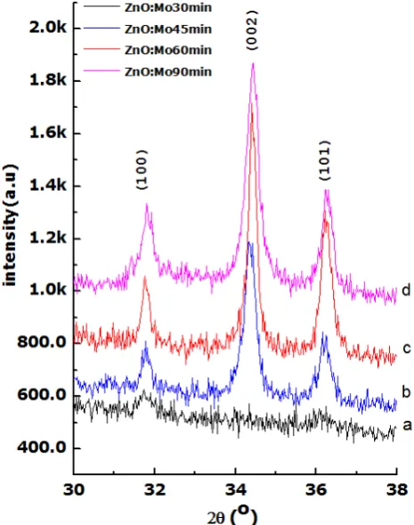
The X-ray diffraction spectra of ZnO films formed at various deposition times on borosilicate substrate are shown in Figure 1a. The XRD spectra were recorded in the 2θ range 30o-80o. The only detected diffraction peaks are located between 30o and 40o. The peaks observed at 32.6o, 34.4o and 36.2.0o correspond to respectively (100), (002) and (101) orientations of zinc oxide.
Figure 1a. X-Ray Diffraction pattern of a Mo-doped ZnO thin film deposited under different time of deposition, a) for 30min, b) for 45min, c) for 60min. and d) for 90min
The intensity of the (100) peak is increasing with the deposition time. The intensity of the (002) and the (101) peaks increases as the deposition time is increased to 60 minutes. This feature of the intensity as function of the deposition time is due to the increased coverage of the substrate and the improvement in the crystalline of the films.
The Full Width at Half Maximum (FWHM) of the (002) peak decreased from 0.29o to 0.21o with the increase of deposition time from 45 min to 60min respectively. However, at long deposition time (d), the (002) and the (101) peaks intensity decreased and the FWHM of the (002) peak increased to 0.33o which may indicate that the film crystallinity is deteriorated. This may be due to the fact that i) there may be an inhomogeneous thickness or grain-size related strain-distribution, or ii) the atoms are not enabled to move to their stable sites as pointed out by some authors in early studies [16].
Figure 1b. Effect of the annealed at 100°C during 2 hours on the crystalline of the films deposited for different time: (a) for 45 min; (b) for 60 min; (a) for 90 min
Figure 2. Effect of the annealed at 100°C during 2 hours on the position of the (002) Bragg peak of the films deposited for different time: (a) for 45 min; (b) for 60 min; (a) for 90 min
The optical properties of the Mo-ZnO film deposited at 300°C on borosilicate glass during 45, 60 and 90 minutes have been studied in the transmission mode. The transmission spectrum in the UV-Visible region of the Mo-ZnO is displayed in Figure 3. The films are highly transparent showing 80% to 83% transmission with a sharp adsorption edge at a wavelength of about 380 nm (3.262 eV), which is very close to the intrinsic band gap of ZnO (3.3 eV) [11]. The oscillation structure in the highly transmitting region is due to interference effects at the various interfaces between the sample, the substrate and the air. Such interferences fringes in the curve indicate well defined good quality interfaces and smooth surfaces [11].
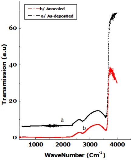
Figure 4 shows the transmittance spectra of the two samples (as-deposited and annealed). After annealing, the films were found to be transparent in the visible region, with a sharp absorption edge at a wavelength of about 380 nm, which is very close to the to the intrinsic band gap of ZnO (3.3 eV). As shown in Figure 3, the increase in the number of the interference fringes with the annealing may be due to decreasing scattering caused by the densification of grains followed by grain growth and the reduction of grain boundary density [17].
Figure 4. Effect of the annealed at 100°C during 2 hours on the Optical transmission spectrum in the wavelength range of 200-900 nm for Mo-doped ZnO films prepared at 300°C during 60 minutes
Figure 5 shows the variation of the optical band gap with the deposition time.
The direct band gap of ZnO thin film was estimated by plotting (α.hν)2 versus (hν) and extrapolating the linear portion near the onset of absorption edge to the energy axis. The optical band gap decreased with increasing deposition time i.e. film thickness.
The optical gap is defined as the minimum energy needed to excite an electron from the valence band to the conduction band. In pure undoped crystals the optical gap equals the energy separation between the band edges. On heavy doping, the donor electrons occupy states at the
bottom of the conduction band, since Pauli principle prevents states from being doubly occupied, the optical band gap is given by the energy difference between the states with Fermi momentum in the conduction and valence band. This type of blocking of low energy transitions is known as Burstein–Moss effect [18,19].
Figure 5. Variation of the optical band gap of Mo-doped ZnO film with the deposition time
The refractive index was estimated by using SWANWPOEL method based on a quantitative analysis of such interferences [20].
Figure 6 shows the variation of the films refractive index as function of the wavelength. A close agreement has been found between our experimental data and a fit based on Sellmeir theory [21].
Figure 7 shows the infrared optical transmittance (500-4000 cm-1) as a function of wavelength for ZnO:Mo films prepared at 300°C deposited on borosilicate glass during 60 minutes. Three spectral regions can be distinguished as follow, the 500-62250 cm-1, the 2250-3650cm-1 and the 3650-4000 cm-1. While the higher spectral region is related with the absorption edge as seen above in the UV-Visible spectrum, the intermediate spectral range exhibit broad bands usually attributed to band tailing associated with disorder, or impurities.
Figure 7. Optical transmission spectra in the Infra-Red wavelength range of 500-4000 cm-1 as function of wavelength for Mo-doped ZnO films
prepared at 300°C during 60 minutes
The as-deposited sample exhibits in the lower-energy range an IR transmission as small as 8%. Futher improvement may be achieved by post deposition thermal annealing, good conducting properties Which need to be optimized.
4. Conclusion
Mo doped Zinc oxide films were deposited on borosilicate glass substrate by Pulsed Laser Deposition (PLD) technique from sintered Zinc Oxide target in an oxygen atmosphere.
A systematic study was made on the structural and optical properties.
X-ray diffraction studies revealed that the films were polycrystalline in nature with (002) orientation normal to the substrate surface, along the c-axis. The samples are experiencing mismatch strain and undergone partial or full
relaxation depending on the thickness most probably below and above the critical layer thickness.
The shift behavior of the XRD peaks before and after annealing reveals that constrains.
It is concluded that the ZnO films formed at 30 minutes of deposition time has a low optical transmittance in the infrared region.
Acknowledgments
This work is sponsored in by African Laser Centre (ALC), the authors are thank full for thier financial support
References
[1] L. Vayssiere, K. Keis & A. Hagfeldt, J. Chem. Mater. 13, p.4395, (2001).
[2] D.S. Ginley & C. Bright, Mater. Res. Bull.25, p.15, (2000). [3] C.G. Granqvist, A. Azens, A. Hjelm, L.Kullman, G.A. Niklasson,
D.Ronnow, M. Stromme Matson, M. Veszlei & G. Vaivars, Sol. Energy. 63 (4), p.199, (1998).
[4] B. Wang, N. Han, D. Meng, R. Yue, J. Yan, & Y. Chen,
Particuology, Volume 9, Issue 3, Pages 253-259 June (2011), [5] X. Jiang, Y. Liu, Y. Gao, X. Zhang, & L. Shi, Particuology, Vol.8,
Issue 4, Pages 383-385 August (2010).
[6] J. Sithole, B.D. Ngom, S. Khamlich, E. Manikanadan, N. Manyala, M.L. Saboungi, D.Knoessen, R. Nemutudi, M. Maaza, Appl. Surf. Sci. (2012).
[7] P. X. Gang, L. Manna & W. Yang, Nature. 404, p.5964, (2000). [8] R.G. Gordon, Mater. Res. Soc. Bull. 25, n°8, p.52, (2000). [9] M. Joseph, H. Tabata & T. Kawai, Jpn. J. Appl. Phys., Part 2:
Lett.38, p. L1205, (1999).
[10] Z.K. Tang, G.K.L. Wong, P.Yu, M. Kawasaki, A. Ohtomo, H. Koinamura & Y. Segawa, Appl. Phys. Letts. 72 (25), p.3270, (1998).
[11] Ü. Özgür, Ya. I. Alivov, C. Liu, A. Teke, M. A. Reshchikov, S. Doğan, V. Avrutin, S.-J. Cho, and H. Morkoç, Journal Of Applied Physics 98, 041301 (2005).
[12] Number Density and Diameter Control of Chemical Bath Deposition of ZnO Nanorods on FTO by Forced Hydrolysis of Seed Crystals Journal of the American Ceramic Society 97 (4), 1028-1034 (2014).
[13] Single Step Integration of ZnO Nano- and Microneedles in Si Trenches by Novel Flame Transport Approach: Whispering Gallery Modes and Photocatalytic Properties ACS Applied Materials & Interfaces 2014 6 (10), 7806-7815.
[14] B. D. Ngom, T. Mpahane, N. Manyala, O. Nemraoui, U. Buttner, J.B. Kana, A.Y. Fasasi, M. Maaza and A.C. Beye, Applied Surface Science, 255, 4153-4158 (2009).
[15] B. D. Ngom, O. Sakho, N. Manyala, J.B. Kana, N. Mlunguisi, L. Gerbous, A.Y. Fasasi, M. Maaza, A.C. Beye, Applied Surface Science,255, 7314-7318 (2009).
[16] Y. Sun, G. M. Fuge, and M. N. R. Ashfold, Chemical Physics Letters, vol. 396, no. 1-3, pp. 21-26, (2004).
[17] Z.K. Tang, G.K.L. Wong, P.Yu, M. Kawasaki, A. Ohtomo, H. Koinamura & Y. Segawa, Appl. Phys. Letts. 72 (25), p.3270, (1998),
[18] B. E. Sernelius, K. F. Berggren, Z. C. Jin, I. Hamberg and C. G. Granqvist, Phys. Rev. B 37 10244 (1988).
[19] E. Jill Roth, Barbara L. Frazier, Nestor R. Apuya and Karl G. Lark, the Genetics Society of America (1989).