ISSN: 1546-9239
©2014 Science Publication
doi:10.3844/ajassp.2014.69.73 Published Online 11 (1) 2014 (http://www.thescipub.com/ajas.toc)
Corresponding Author: Praveena Murugesan, Department of ECE, Anna University, Tamilnadu,India
AN IMPROVED DESIGN OF REVERSIBLE BINARY
TO BINARY CODED DECIMAL CONVERTER
FOR BINARY CODED DECIMAL MULTIPLICATION
1
Praveena Murugesan and
2Thanushkodi Keppanagounder
1Department of ECE, Anna University, Tamilnadu, India 2
Akshaya College of Engineering and Technology, Coimbatore, Tamilnadu, India Received 2012-09-17; Revised 2013-09-19; Accepted 2013-11-28
ABSTRACT
Reversible logic gates under ideal conditions produce zero power dissipation. This factor highlights the usage of these gates in optical computing, low power CMOS design, quantum optics and quantum computing. The growth of decimal arithmetic in various applications as stressed the need to propose the study on reversible binary to BCD converter which plays a greater role in decimal multiplication for providing faster results. The different parameters such as gate count,garbage output and constant input are more optimized in the proposed fixed bit binary to binary coded decimal converter than the existing design. Keywords: Reversible Logic, BCD Multiplication, Quantum Computing, Nanotechnology
1. INTRODUCTION
The electronic industry faced a greater challenge to decrease the energy dissipation of circuits along with the wide advancements in the era of integrated circuits. The above fact is the main reason for designing reversible logic gates for reducing the power dissipation which in recent years has gained greater momentum.
According to the principle of Landauer (1961), the conventional combinational logic circuits dissipate energy due to the information loss in the process. The energy dissipation of KTln2 joules occurs for each bit of information where K is the Boltzmann’s constant of 1.38×10⁻²³ J/K and T is the absolute temperature at which the computations are performed. This dissipation has got greater impact on the life and speed of CMOS devices. Many researchers demonstrated that the energy dissipation can be kept under control by the introduction of reversible logic gates.
A reversible logic gate is a k-input and k-output device (denoted k*k) where inputs must be equal to its outputs. Reversible gate can generate unique output pattern for each input vector and vice versa i.e., there is
correlation between each of its input and output assignment (Haghparast and Navi, 2008a). Since the usage of fanouts are disallowed in the reversible logic circuits, additional logic gates can be introduced inorder to achieve the required result. The parameters that are used in the measurement of performance and complexity of reversible logic circuits are as follows (Haghparast and Navi, 2008b):
• Number of reversible gates • Quantum cost
• Hardware Complexity • Constant inputs and • Garbage outputs
Decimal arithmetic has its wide usage in financial and commercial applications. It plays greater role in these applications because of its high level of accuracy but it is slower than binary arithmetic. This led to the need for determining standard specifications for decimal floating-point arithmetic. Thus the new revision of the IEEE standard (IEEE 754-2008) includes specifications for decimal floating point arithmetic (Ahmed, 2011).
In this study an improved design of reversible binary to BCD converter is introduced. The usage of n bit converters for fixed bit binary to Binary Coded Decimal conversion is expensive in terms of gate count and quantum cost. Therefore a 7 bit binary to 8 bit BCD converter is introduced in this study. This technique produces better results when compared with the earlier works done in reversible binary to BCD converter.
The structure of this study is as follows. Firstly this study introduces the reversible gates required in the implementation of the proposed design. Secondly the proposed reversible gates are described. Then the proposed architecture details are mentioned with an examples and finally the comparative analysis is done.
2. MATERIALS AND METHODS
2.1. Basic Reversible Logic Gates
The reversible logic gates required in the implementation of reversible binary to BCD converter are discussed below.
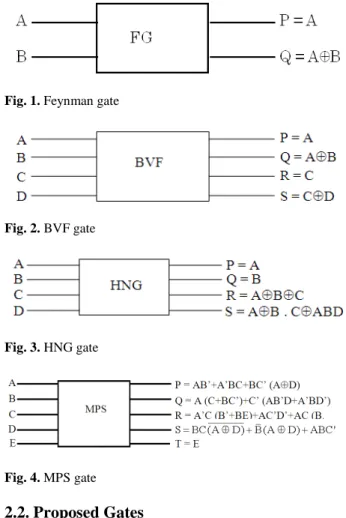
A 2*2 Feynman gate (Feynman, 1986) also called Controlled NOT is shown in Fig. 1. It is a basic gate which is used to copy a input and to invert a input bit. The Input vector Iv and the Output vector Ov of Feymann gate are Iv = (A, B) and the Ov = (P = A, Q = A ⊕ B) respectively .
A reversible 4*4 BVF gate (Bhagyalakshmi and Venkatesha, 2010) in Fig. 2 contains XOR gate at the output Q and S. Therefore it allows for the duplication of the inputs inorder to overcome the fanout which is not allowed in reversible circuits. In contrast to FG gate where duplication of single input takes place, in BVF gate duplication of both the inputs are done. Consider for example, the Input vector IV = (1,0,1,0) then the output vector becomes OV = (1,1,1,1).
A single HNG gate (Haghparast and Navi, 2008b) can implement all the functions of a reversible full adder unit which is depicted in Fig. 3. This gate produces two garbage outputs and requires one constant input to function as a full adder unit. Therefore in a 4 bit adder it has 8 garbage outputs and 4 constant inputs which is considered to be minimal.
The 5*5 reversible MPS gate (Praveena and Thanushkodi, 2012) can work as BCD detection and correction gate is depicted in Fig. 4. When the outputs are greater than 1001 (9) then MPS gate detects it and corrects it with the addition of 0110(6).
Fig. 1. Feynman gate
Fig. 2. BVF gate
Fig. 3. HNG gate
Fig. 4. MPS gate
2.2. Proposed Gates
Two reversible gates Binary Coded Decimal Higher significant digit (BCDH) and Binary Coded Decimal Lower significant digit (BCDL) are proposed in this study to convert the higher significant binary bits to its valid BCD digit. Consider the seven binary bits b6b5b4b3b2b1b0 to be converted into Binary Coded Decimal digits. In this b6b5b4 are higher significant binary bits. These b6b5b4 (HSBs) bits contribute differently towards the lower and higher significant BCD digits. The below equation clearly explains the contribution of the b6b5b4 bits:
b6×26 + b5×25 + b4×24
For example consider 011(HSB), by the above equation the value will be 48 which is represented as 0100 and 1000 where 0100 is higher significant BCD digit and 1000 is lower significant BCD digit.
Truth table of BCDH and BCDL gate can be drawn from the logic function representation and it will clearly
show that the gates are reversible by having unique output for each of its input. This verifies the criteria of reversible logic gates.
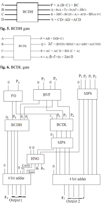
2.3. BCDH Gate
The proposed BCDH gate in Fig. 5 is a 4*4 reversible logic gate. The gate can be used to obtain the higher significant Binary Coded Decimal digit from the higher significant binary bits. For example when the input to BCDH gate is 0100 (Higher significant binary bits) then the output obtained from this gate is 0110.
The logic function representation of the gate is shown below: P = ∑m (6,7,10,11,12,13,14,15) Q = ∑m (3,4,5,9,12,13,14,15) R = ∑m (2,4,5,7,8,11,14,15) S = ∑m (1,2,5,6,9,11,13,15)
2.4. BCDL Gate
The 4*4 BCDL gate is used to derive the lower significant BCD digits from the higher significant binary bits is depicted in Fig. 6. When input to BCDL gate is 0100 (Higher significant binary bits) then the output obtained from BCDL gate is 0100.
The logic function representation of the gate is as shown below: P = ∑m (3,5,7,11,12,13,14,15) Q = ∑m (1,4,7,9,10,13,14,15) R = ∑m (1,2,5,8,10,11,14,15) S = ∑m (6,8,9,10,11,12,13,15)
2.5. Proposed Architecture
The proposed reversible binary to BCD converter architecture is a alteration of the architecture in (Bhattacharya et al., 2010) to make it appropriate for reversible logic execution. The reversible 7 bit binary to 8 bit BCD converter architecture is shown in Fig. 7.
Consider binary bits b6b5b4b3b2b1b0 which are to be converted to BCD bits c7c6c5c4c3c2c1c0. The lower significant binary bits b3b2b1b0 are sent through the MPS gate where the BCD detection and correction takes place. This gate adds the correction factor 0110, when the bits are greater than 1001.
The higher significant binary bits b6b5b4 are duplicated by the usage of BVF and FG gates. Bits b4 and b5 are duplicated by the BVF gate and b6 is copied by the usage of FG gate.
Fig. 5. BCDH gate
Fig. 6. BCDL gate
Fig. 7. Architecture of reversible 7 bit binary to 8 bit BCD converter
These two sets of b6b5b4 are sent to the BCDH and BCDL gates respectively. From these gates the higher and lower significant BCD digits are obtained. The multiplication of two BCD digits will ultimately result only in the following combinations of b6, b5 and b4 and they are 000, 001, 010, 011, 100 and 101 (Bhattacharya et al., 2010). Based on the above logic the reversible BCDH and BCDL gates are designed.
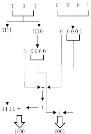
Fig. 8. Example of a binary to BCD conversion Final result is 1000 0001
The outputs of BCDL are checked for the needed BCD correction through the MPS gate,and the carry that is obtained is added with the carry obtained from the lower significant binary bits through the HNG gate. Then the possible sum and carry is added with the higher significant BCD digit through the 4 bit adders. The outputs of both the MPS gates are added to obtain the BCD bits c3c2c1c0. The ultimate output c7c6c5c4c3c2c1c0 comes from both the 4 bit adders.
For example consider the structure of a binary number (1010001)2 being transferred to its corresponding BCD digit that is 1000 0001 in Fig. 8.
3. RESULTS
Table 1 analysis the details of reversible 7 bit binary to 8 bit BCD converter and Table 2 clearly compares the proposed circuit with the existing design.
The Table 1 clearly shows the number of gates, number of constant inputs and number of garbage outputs that are used in the designing of the binary to BCD converter.
Table 1. Analysis of proposed reversible 7 bit binary to 8 bit BCD converter
No of No. of No. of
Gate reversible gates constant inputs Garbage outputs
HNG 9 14 20 MPS 2 2 0 BVF 1 2 0 FG 1 1 0 BCDH 1 1 0 BCDL 1 1 0 Total 15 21 20
Table 2. Comparative analysis of Various Reversible Binary to BCD converter
Reversible binary No. of No. of to BCD No. of constant garbage
converter gates inputs outputs Delay
Raj mohan 49 61 64 49
Rajmohan et al. (2010)
Proposed 15 21 20 15
It is evident from the above table, that the proposed architecture uses a total of 15 reversible logic gates, 21 inputs and 20 garbage outputs.
The proposed binary to BCD converter performs better than the existing circuits. Table 2 proves the above fact.
4. DISCUSSION
Minimizing the number of reversible gates is the major constraint in designing reversible logic circuits. The proposed circuit uses a total of 15 reversible gates,which shows a clear improvement of 69.3% over the existing circuit (Rajmohan et al., 2010).
In reversible logic circuits the total delay of the proposed circuit is calculated in terms of gate delays. The total delay ∆ is:
∆Total = ∆MPS+∆HNG+∆BVF+∆FG+∆BCDH + ∆BCDL
∆ Total = 2 + 9 + 1 + 1 + 1 + 1 = 15 Gate delays The other important criterion in designing reversible binary to BCD converter is to lessen the number of constant inputs so as to increase the performance of the circuits. Therefore the proposed circuit is designed with an improvement of 65.5% over the existing design.
Another criterion to be considered is the garbage output. The cost of the circuit increases for every
garbage bit. Therefore it is kept minimal at 20 and shows 68.7% improvement over the other circuit.
5. CONCLUSION
This study presented an improved design of reversible binary to BCD converter to be used in decimal multiplication. The proposed converter reduces the overall cost of the circuit by reducing the number of gates and by optimizing other essential parameters. Though computations on reversible binary to BCD converter requires double the steps when compared to conventional combinational circuits they are very much required for many applications especially quantum computing where only reversible gates are employed in the architecture. This design will be useful in building more complex computational structures and can be used as a base for future research in designing a very optimized reversible BCD multiplier.
6. REFERENCES
Ahmed, M.E.E., 2011. Decimal floating point arithmetic unit based on a fused multiply add module. MS Thesis, Electronics and Communication Engineering.
Bhagyalakshmi, H.R. and M.K. Venkatesha, 2010. An improved design of a multiplier using reversible logic gates. Int. J. Eng. Sci. Technol., 2: 3838-3845.
Bhattacharya, J., A. Gupta and A. Singh, 2010. A high performance Binary to BCD converter for decimal multiplication. Proceedings of the International Symposium on VLSI Design Automation and Test, Apr. 26-29, IEEE Xplore Press, Hsin Chu, pp: 315-318. DOI: 10.1109/VDAT.2010.5496752
Feynman, R., 1986. Quantum mechanical computers. Found. Phys., 16: 507-531.
Haghparast, M. and K. Navi, 2008a. A novel fault tolerant reversible gate for nanotechnology based systems. Am. J. Applied Sci., 5: 519-523. DOI: 10.3844/ajassp.2008.519.523
Haghparast, M. and K. Navi, 2008b. A novel reversible BCD adder for nanotechnology based systems. Am. J. Applied Sci., 5: 282-288. DOI: 10.3844/ajassp.2008.282.288
Landauer, R., 1961. Irreversibility and heat generation in the computing process. IBM J. Res. Dev., 5: 183-191. DOI: 10.1147/rd.53.0183
Praveena, M. and K. Thanushkodi, 2012. A novel design of reversible BCD adder with reduced delay. Eur. J. Scient. Res., 83: 282-288.
Rajmohan, V., V. Ranganathan and M. Rajmohan, 2010. A reversible design of BCD multiplier. J. Comput., 2: 112-117.