Implementation of RISC Processor for DSP Accelerator Architecture
Exploiting Carry Save Arithmetic
Lanke Kalyani1, A.Sowjanya2, M. Nagendra Kumar3 M.Tech (student)1,Assistant Professor2,HOD & Associate professor3
1VLSI & Embedded systems,1,2,3Dept.of Electronics and Communication Engineering
Kakinada Institute of Engineering and Technology for Women, Korangi,AP,INDIA
Abstract— Hardware increasing speed has been demonstrated a to a great degree promising usage system for the advanced flag processing(DSP) area. Instead of receiving a solid application-particular coordinated circuit configuration approach, in this brief, we exhibit a novel quickening agent engineering including adaptable computational units that bolster the execution of a vast arrangement of operation formats found in DSP pieces. We separate from past takes a shot at adaptable quickening agents by empowering calculations to be forcefully performed with convey save(CS) organized information. Propelled number juggling plan ideas, i.e., recoding methods, are used empowering CS improvements to be performed in a bigger degree than in past methodologies. Broad exploratory assessments demonstrate that the proposed quickening agent design conveys normal an in so fup to 61.91%in range defer item and 54.43% in vitality utilization contrasted and the condition of-craftsmanship adaptable information ways. In this paper, their fixation is on 16 bit operations yet here in the proposed conspire, the emphasis is on 32 bit operations. Hardware Acceleration fundamentally alludes to the use of PC hardware to play out a few capacities speedier than they are really conceivable inside the product running on broadly useful CPU. The RISC or Reduced Instruction Set Computer is a plan logic that has turned into a standard in Scientific and designing applications. The fundamental target of this paper is to outline and execute of 32– bit RISC(Reduced Instruction Set Computer) processor for adaptable DSP Accelerator Architecture. The outline will enhance the speed of the processor, and to give the higher execution of the processor. The most vital featureofthe RISC processor is that this processor is exceptionally basic and bolster stack/store engineering. The critical segment delicate his processor incorporate the Arithmetic Logic Unit, Shifter, Rotator and Control unit. The module usefulness and execution issues like territory, power dissemination and spread postponement are examined. Along these lines, here we meet a portion of the primary limitations like Complexity of the direction set, which will lessen the
measure of space, time, cost, power, warm and different things that it takes to actualize the guideline set part of a processor. As the Time of execution reductions, the Speed of execution naturally increments.
IndexTerms—Hardware Acceleration, Reduced Instruction Set Computer (RISC), Carry Save formatted Data.
I.INTRODUCTION
Advanced embedded frameworks target top of the line application areas requiring productive usage of computationally serious computerized flag handling (DSP) capacities. The consolidation of heterogeneity through particular equipment quickening agents enhances execution and diminishes vitality utilization. Despite the fact that application-particular coordinated circuits(ASICs) frame the perfect speeding up arrangement as far as execution and power, their firmness prompts to expanded silicon unpredictability, as numerous instantiated ASICs are expected to quicken different bits.
Numerous analysts have proposed the utilization of space particular coarse-grained reconfigurable quickening agents to build ASICs' adaptability without fundamentally bargaining their execution. Superior adaptable information ways have been proposed to effectively outline or fastened operations found in the underlying information stream graph(DFG) of a bit. The formats of complex tied operations are either separated specifically from the bit's DFG or determined in
fastening. As of late, Ansalonietal. Received forceful operation binding to empower the calculation of whole sub expressions utilizing various ALUs with heterogeneous number juggling highlights. DSP part gives a rich arrangement of C-callable deterministic bit benefits that empower designers to make complex applications without bargaining constant due dates. DSP piece is very versatile with multithreading arrangements requiring as few as 1K words.
The a fore specified reconfigurable designs reject number juggling enhancements amid the building union and consider the monly at the inward circuit structure of primitive segments, e.g.,adders, amid the rationale synthesis[11].However, inquire about exercises have demonstrated that the number-crunching advancements at higher deliberation levels than the auxiliary circuit one altogether affect on the information way execution. In[12],timing-driven optimizationsbasedoncarry-save(CS) number juggling were performed atthe post-Register Transfer Level (RTL) outline arrange. In [13], normal sub expression end in CS calculations is utilized to upgrade direct DSP circuits. Vermaetal.[14] created change systems on the application's DFG to amplify the utilization of CS number-crunching earlier the genuine information way blend. DSP piece arrangement should be possible either statically through graphical or scripting devices or powerfully utilizing working framework calls. Notwithstanding barring unused modules, static setup additionally diminishes target memory impression by dispensing with the code required to powerfully make and erase working framework questions, for example, strings and semaphores.
The a for ementioned CS enhancement approaches focus in adaptable information way, i.e., ASIC, usage. As of late, Xydisetal .proposed an adaptable design consolidating the ILP and pipelining methods with the CS-mindful operation tying. In any case, all the a for ementioned arrangements highlight an inborn constraint, i.e., CS improvement is limited to combining just increases/subtractions. ACS to Binary transformation is embedded before every operation that contrasts from expansion/subtraction, e.g., increase, along these lines, distributing various CS to double changes that intensely debases execution because of tedious convey proliferations. In this brief, we propose a superior design conspire for the blend of adaptable equipment DSP quickening agents by consolidating advancement methods from both the engineering and number juggling levels of reflection. We present a flexibled at a way engineering that
proposed quickening agent design conveys normal additions of up to 61.91% in range postpone item and 54.43% in vitality utilization contrasted with condition of-craftsmanship adaptable information ways managing proficiency toward scaled innovations.
II. CARRY-SAVE ARITHMETIC
CS representation has been widely used to design fast arithmetic circuits due to its inherent advantage of eliminating the large carry-propagation chains. CS arithmetic optimizations rearrange the application’s DFG and reveal multiple input additive operations(i.e., chained additions in the initial DFG), which can be mapped onto CS compressors. The go a list to maximize the range that a CS computation is performed with in the DFG. How ever, when ever a multiplication node is in terleaved in the DFG, either a CS to Binary conversion is in vokedor the DFG is transformed using the distributive property. Hence, the in advance of said CS improvement approaches have restricted effect on DFGs ruled by duplications, e.g., separating DSP applications. In this brief, we handle the before said confinement by abusing the CS to Modified Booth(MB) recoding every time a duplication should be performed with in a CS-streamlined information way. In this manner, the calculations all through the duplications are prepared utilizing CS number juggling and the operations in the focused on information way are done without utilizing any halfway convey spread snake for CS to Binary change, in this manner enhancing execution.
The proposed adaptable quickening agent engineering is appeared in Fig.1. Each FCU works specifically on CS operands and produces information in a similar frame for direct reuse of bury intervene comes about. Each FCU works on 16-bit operands. Such a bit-length is adequate for the most DSP data paths, but the architectural concept of the FCU can be straight forwardly adapted for smaller or larger bit-lengths.
The number of FCUs is determined at design time based on the ILP and are a constraints imposed by the designer. The CS to B in module is a ripple-carry adder and converts the CS form to the two’s complement one. The register bank consists of scratch registers and is used for storing intermediate results and sharing operands among the FCUs. Different DSP kernels(i.e., different register allocation and data communication patterns per kernel)can be mapped onto the proposed architecture using post-RTL data path interconnection sharing techniques.
The control unit drives the overall architecture (i.e., communication between the data port and the register bank, configuration words of the FCUs and selection signals for the multiplexers)in each clock cycle. In this paper, we are introducing the 32 bit RISC Processor for 32 bit arithmetic and logical operations. The RISC processor architecture consistsof Arithmetic Logic Unit (ALU), Control Unit (CU),Barrel Shifter, Booth’s Multiplier, Register File andAccumulator. RISC processor is composed with load/store (Von Neumann) engineering, implying that all operations are performed on operands held in the processor registers and the principle memory must be gotten to through the heap and store directions. One shared memory for instructions(program) and information with one information transport and one address transport amongst processor and memory.
Guideline and information are gotten in consecutive request so that the inactivity brought about between the machine cycle output be diminished. For expanding the speed of operation RISC processor is composed with five phase pipelining. The pipelining stages are Instruction Fetch (IF), Instruction Decode (ID), Execution (EX), Data Memory (MEM), and Write Back(WB).
A. Structure of Flexible Computational Unit
The structure of the FCU (Fig. 2)has been intended to empower elite adaptable operation binding in light of a library of operation formats. Each FCU can be arranged to any of the T1–T5 operation formats appeared in Fig.3. The proposed FCU empowers intra layout operation tying by intertwining the increments performed before/after the increase and plays out any incomplete operation format of the accompanying complex operations:
W∗= A ×(X∗+Y∗)+K∗(1)
W∗=A ×K∗+(X∗+Y∗). (2)
The multiplier contains a CS-to-MB module, which receives an as of late proposed strategy to recode the 33-bit P∗in its individual MB digits with insignificant convey proliferation. The multiplier's item comprises of 33bits.The multiplier incorporates a pay strategy for lessening the blunder forced at the item's exactness by the truncation system. However, since all the FCU inputs consist of 32bits and provided that there are no over flows,
the 32 most significant bits of the 33-bit W∗(i.e., the out put of the Carry-Save Adder (CSA) tree, and thus, of the FCU) are embedded in the appropriate FCU when requested. In this paper we are including Shifting, Increment & Decrement and Logical basic gates operations using the RISC instruction set.The system architecture of a 32 - bit RISC processor is shown in Fig. 3.
In order to efficiently map DSP kernels onto the proposed FCU-based accelerator, the semiautomatic synthes is methodology presented in has been adapted. At first, a CS-aware transformation is performed onto the original DFG, merging nodes of multiple chained additions/subtractions to 4:2 compressors. A pattern generation on the transformed DFG clusters the CS nodes with the multiplication operations to form FCU template operations (Fig.4). The designer selects the FCU operations covering the DFG for minimized latency.
Given that the number of FCUs is fixed, are source-constrained scheduling is considered with the available FCUs and CS to B in modules determining there source constraint set. The clustered DFG is scheduled, so that each FCU operation is assigned to a specific control step. Alist-based scheduler[21] has been adopted considering the mobility of FCU operations. The FCU operations are scheduled according to descending mobility. The scheduled FCU operations are bound onto FCU instances and proper configuration bits are generated. After completing register allocation, a FSM is generated in order to implement the control unit of the over all architecture.
IV. THE ORETIC LANALYSIS
V.EXPERIMENTALEVALUATION
A. Circuit-Level Exploration of the Proposed FCU With Respect to Technology Scaling
A circuit-level comparative study was conducted among the proposed FCU, the flexible computational component(FCC) and there configurable arithmetic unit(RAU) of in scaled technology nodes. The CS representation requires twice the number of bits of the respective two’s complement form, thus, increasing wiring and affecting performance in scaled technologies. This experimentation targets to show that the scaling impact on the performance does not eliminate the benefits of using CS arithmetic. The three units considered were described in RTL using Verilog. The CSA tree of the proposed FCU and the adders and multipliers of the FCC were imported from the Synopsys Design Ware library. We used Synopsys Design Compiler to synthe size the examined units and the TSMC130,90, and 65nm standard cell libraries. We synthesized each unit with the highest optimization degree at its critical clock period and 20 higher ones with a step interval of 0.10ns. Fig.6 reports the area complexity of the evaluated units at130,90, and 65nm of synthes is technology.
At 130nm, the proposed FCU, the FCC, and the RAU operate with out timing violations starting at 2.98, 4.83, and 1.99ns, respectively. At 90nm, the proposed FCU, the FCC, and the RAU are timing functional starting at1.66,2.46, and 1.01ns, respectively. In addition, at 65nm, the proposed FCU, the FCC, and the RAU start operating with out timing violations at 1.13,1.68, and 0.67ns, respectively. As the synthes is technology is scaled down, Fig.6 shows that the proposed FCU out performs the FCC in terms of critical delay and are a complexity, but presents larger values for these metrics than the RAU in all the
technology nodes. How ever, RAU’s flexible pipe line stage(FPS) features limited ability in carrying out heavy arithmetic operations as shown from them ega operations per second/watt (MOPS/W) evaluationinFig.7.
Fig. 7 shows the MOPS/W values for the proposed FCU, the FCC, and the RAU at their critical clock periods with respect to the synthes is technology. For each unit, we consider the templates with the largest number of active operations with out over lapping the one another and calculate the average((#Ops)/(#Cycles)) factor. The #Ops derives from the two’s complement arithmetic operations (additive or multiplicative). For CS-aware units, i.e., FCU and RAU, the CS to Bin module runs in parallel with the FCU or RAU, thus counting as one additive operation. In particular, for the proposed FCU, we consider the templatesT1 (or T2) with six operations (e.g., five operations from T1 and one operation from CS to Bin) in one cycle and T3 with five operations in one cycle.
triggered. As shown, the proposed FCU delivers average MOPS/W gains across technology nodes of 6× and2× over FCC and RAU, respectively. Thus, as the synthesis technology is scaled down, the benefit soft he proposed FCU remain.
B.MappingofDSPKernelsontothePropos edFCU-BasedArchitecture
We examined the efficiency of the proposed solution by mapping and accelerating DSP kernels on to the FCU data path, that is:
1) A sixth-order ELLIPTIC filter;
2) A 16-taps Finite Impulse Response filter (FIR16); 3) A non linear IIR VOLTERRA filter;
4) An 1-D unrolled Discrete Cosine Transform (DCT) kernel(UDCT);
5) The2-D JPEG DCT (JPEGDCT) [25]; and 6) The2-D Inverse MPEGDCT (MPEG_IDCT).
The kernels were scheduled and mapped onto the architectures based on the pro- posed FCU, the FCC [4], and the RAU. The proposed architecture comprises four FCUs and one CS to Bin module, the FCC-base done contains two FCCs(=8ALUs+8Multipliers), and the RAU-based architecture consists off our FPSs and one CS to Bin module. For each kernel mapped, the maximum memory band width has been allocated between the local storage and the processing elements. All the data paths were synthesized at 65nm. The clock periods were specifiedat 1.60, 2.20, and 1.20 ns for the proposed FCU-,the FCC-,and the RAU- based architectures, respectively, considering the critical delays of Section V-A plus a slack of 0.50ns for absorbing any delays embedded by the multiplexers and control units. Energy consumption values were calculated through Prime Time-PX after simulating each data path with Model sim.
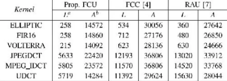
Table I reports the execution latency, area complexity, and energy values of the DSP kernels mapped on to the examined architectures. The execution at ency is the total number of cycles multiplied by the clock period for the synthes is of each architecture. The average latency gains of the proposed FCU-based architecture over the ones built on the FCC and the RAU are 33.36% and 56.69%, respectively. Regarding the area complexity, the proposed FCU-based flexible at a path delivers average gains of31.75%and13.23%overthe FCC-and RAU-based solutions, respectively. As shown, different kernels demand different are a resources due to the differing needs
of the area-delay product and the energy providing a clear view of the beneficial characteristics of the proposed approach and allowing us to safely conclude that the proposed architecture forms a very efficient solution for DSP acceleration.
TABLE III
VI.CONCLUSION
A 32-bit RISC processor with 16 instruction set has been designed. Every instruction is executed in one clock cycles with 5-stage pipelining. The design is verified through exhaustive simulations. The processor achieves higher performance, lower area and lower power dissipation for flexible DSP accelerator architecture. This processor can be used as a systolic core to perform mathematical computations like solving polynomial and differential equations. In this brief, we introduced a flexible accelerator architecture that exploits the in corporation of CS arithmetic optimizations to enable fast chaining of additive and multiplicative operations. The proposed flexible accelerator architecture is able to operate on both conventional two’s complement and CS-formatted data operands, thus enabling high degrees of computational density to be achieved. The oretical and experimental analyses have shown that the proposed solution forms an efficient design trade off point delivering optimized latency/area and energy implementations.
REFERENCES
1) P. Ienne and R. Leupers, Customizable Embedded Processors: Design Technologies and Applications. SanFrancisco, CA, USA: MorganKaufmann,2007.
2) P.M. Heysters, G.J.M.Smit, and E.Molenkamp, “Aflexible and energy-efficient coarse-grained reconfigurable architecture for mobile systems,” J.Supercomput.,vol.26,no.3,pp.283–308,2003.
3) B. Mei, S. Vernalde, D. Verkest, H. D. Man, and R. Lauwereins, “ADRES: Anarchitecture with tightly coupled VLIW processor and coarse-grained reconfigurable matrix,”in Proc.13th Int. Conf. Field Program. LogicAppl.,vol.2778.2003,pp.61–70.
4) M. D. Galanis, G. The odorid is, S. Tragou das, and C.E. Gout is, “A high-performance data path for synthe sizing DSP kernels,” IEEE Trans.Comput.-Aided Design Integr. Circuits Syst., vol. 25, no. 6, pp.1154–1162,Jun.2006.
5) K. Compton and S.Hauck, “Automatic design of reconfigurable domain- specific flexible cores,” IEEET rans. Very Large Scale Integr.(VLSI) Syst.,vol.16,no.5,pp.493–503,May2008.
6) S.Xydis, G.Economakos, and K.Pekmestzi, “Designing coarse-grain reconfigurable architectures by inlining flexibility into custom arithmetic data-paths,” Integr., VLSIJ.,vol.42,no.4,pp.486– 503,Sep.2009.
7) S.Xydis, G.Economakos, D.Soudris, and K.Pekmestzi,“High perfor-mance and area efficient flexible DSP data path synthesis,”IEEE Trans. Very Large Scale Integr. (VLSI) Syst.,vol. 19,no. 3, pp. 429–442, Mar.2011.
8) G.Ansaloni, P.Bonzini, and L.Pozzi, “EGRA: A coarse grained reconfigurable architectural template,” IEEE Trans. Very Large Scale Integr. (VLSI)Syst.,vol.19,no.6,pp.1062–1074,Jun.2011.
9) M.Stojilovic ,D.Novo, L.Saranovac, P.Brisk, and P.Ienne, “Selective flexibility: Creating domain-specific reconfigurable arrays,” IEEE Trans. Comput.-Aided Design Integr. Circuits Syst.,vol.32,no.5,pp.681–694, May2013.
10) R.Kastner, A.Kaplan, S.O.Memik, and E.Bozorgzadeh, “Instruction generation for hybrid reconfigurable systems,” ACM Trans. DesignAutom.Electron.Syst.,vol.7,no.4,pp.605– 627,Oct.2002.
11) T. Kim andJ. Um, “A practical approach to the synthesis of arithmetic circuits using carry-save-adders,” IEEE Trans. Comput.-Aided Design Integr. Circuits Syst., vol. 19,no. 5, pp. 615–624, May2000.
12) A.Hosangadi, F.Fallah, and R.Kastner,“Optimizing high speed arithmetic circuits using three-term extraction,” inProc. Design, Autom. Test Eur. (DATE), vol.1.Mar.2006, pp.1–6.
Comput.-Aided Design Integr. CircuitsSyst.,vol.27, no. 10, pp.1761–1774,Oct.2008.
14) B.Parhami, Computer Arithmetic: Algorithms and Hardware Designs. Oxford, U.K.: OxfordUniv.Press,2000.
15) G. Constantinides, P. Y. K. Cheung, and W. Luk, Synthesis and Optimization DSP Algorithms. Norwell, MA, USA: Kluwer, 2004.
16) N.Moreano, E.Borin, C.deSouza, and G.Araujo, “Efficient data- path merging for partially reconfigurable architectures,” IEEE Trans. Comput.-Aided Design Integr. CircuitsSyst.,vol. 24,no.7,pp.969–980, Jul.2005.
17) S.Xydis, G.Palermo, and C.Silvano,“Thermal-aware data path merging for coarse-grained reconfigurable processors,”in Proc.Design, Autom. Test Eur. Conf. Exhibit. (DATE),Mar.2013,pp.1649–1654.
18) K. Tsoumanis, S. Xydis, C. Efstathiou, N. Moschopoulos, and K.Pekmestzi, “An optimized modified booth recoder for efficient design of the add-multiply operator,” IEEE Trans. CircuitsSyst.I,Reg.Papers, vol.61,no.4,pp.1133– 1143,Apr.2014.
19) Y.-H.ChenandT.-Y.Chang,“Ahigh-accuracy adaptive conditional- probability estimator for fixed-width booth multipliers,”IEEE Trans. Circuits Syst. I, Reg. Papers,vol. 59, no. 3, pp. 594–603, Mar.2012.
20) G.D.Micheli, Synthesis and Optimization of Digital Circuits, 1sted. New York,NY,USA: McGraw-Hill,1994.