Serial Infrared Transceiver SIR, 115.2 kbit/s, 2.4 V to 5.5 V Operation
TFBS4711
Vishay Semiconductors
DESCRIPTION
The TFBS4711 is a low profile, infrared data transceiver
module. It supports IrDA
®data rates up to 115.2 kbit/s (SIR).
The transceiver module consists of a PIN photodiode, an
infrared emitter (IRED), and a low-power CMOS control IC to
provide a total front-end solution in a single package.
The device is designed for the low power IrDA standard with
an extended range on-axis up to 1 m. The RXD output pulse
width is independent of the optical input pulse width and
stays always at a fixed pulse width thus making the device
optimum for standard endecs. TFBS4711 has a tri-state
output and is floating in shut-down mode with a weak pull-up.
The shut down (SD) feature cuts current consumption to
typically 10 nA.
APPLICATIONS
• Ideal for battery operated devices
• PDAs
• Mobile phones
• Electronic wallet (IrFM)
• Notebook computers
• Digital still and video cameras
• Printers, fax machines, photocopiers, screen projectors
• Data loggers
• External infrared adapters (dongles)
• Diagnostics systems
• Medical and industrial data collection devices
• Kiosks, POS, point and pay devices
• GPS
• Access control
• Field programming devices
FEATURES
• Compliant with the latest IrDA physical layer low
power specification (9.6 kbit/s to 115.2 kbit/s)
• Small package (H x L x W in mm): 1.9 x 3 x 6
• Typical link distance on-axis up to 1 m
• Battery and power management features:
> Idle current - 70 µA typical
> Shutdown current - 10 nA typical
> Operates from 2.4 V to 5.5 V within specification over full
temperature range from - 25 °C to + 85 °C
• Remote control - transmit distance up to 8 m
• Tri-state receiver output, floating in shutdown with a weak
pull-up
• Constant RXD output pulse width (2.2 µs typical)
• Meets IrFM fast connection requirements
• Split power supply, an independent, unregulated supply for
IRED anode and a well regulated supply for V
CC• Directly interfaces with various super I/O and controller
devices and encoder/decoder such as TOIM4232 or
TOIM5232
• Qualified for lead (Pb)-free and Sn/Pb processing (MSL4)
• Compliant to RoHS directive 2002/95/EC and in
accordance to WEEE 2002/96/EC
20208
PARTS TABLE
PART NUMBER DESCRIPTION QTY/REEL
TFBS4711-TR1 Oriented in carrier tape for side view surface mounting 1000 pcs TFBS4711-TR3 Oriented in carrier tape for side view surface mounting 2500 pcs TFBS4711-TT1 Oriented in carrier tape for top view surface mounting 1000 pcs
TFBS4711
Vishay Semiconductors
Serial Infrared Transceiver SIR, 115.2 kbit/s,
2.4 V to 5.5 V Operation
FUNCTIONAL BLOCK DIAGRAM
PINOUT
TFBS4711
weight 50 mg
Definitions:
In the Vishay transceiver datasheets the following
nomenclature is used for defining the IrDA operating modes:
SIR: 2.4 kbit/s to 115.2 kbit/s, equivalent to the basic serial
infrared standard with the physical layer version IrPhy 1.0
MIR: 576 kbit/s to 1152 kbit/s
FIR: 4 Mbit/s
VFIR: 16 Mbit/s
MIR and FIR were implemented with IrPhy 1.1, followed by
IrPhy 1.2, adding the SIR low power standard.
PRODUCT SUMMARY
PART NUMBER DATA RATE
(kbit/s) DIMENSIONS H x L x W (mm) LINK DISTANCE (m) OPERATING VOLTAGE (V) IDLE SUPPLY CURRENT (mA) TFBS4711 115.2 1.9 x 3 x 6 0 to 0.7 2.4 to 5.5 0.07 18282 Controlled driver Push-pull driver GND TXD RXD VCC2 VCC1 Amplifier Comparator SD Logicand control REDC 19428 PIN 1
PIN DESCRIPTION
PINNUMBER SYMBOL DESCRIPTION I/O ACTIVE
1
VCC2 IRED anode
Connect IRED anode directly to the power supply (VCC2). IRED current can be decreased by adding a resistor in series between the power supply and IRED anode. A separate
unregulated power supply can be used at this pin
2 TXD
This Schmitt-Trigger input is used to transmit serial data when SD is low. An on-chip protection circuit disables the LED driver if the TXD pin is asserted for longer than 100 µs.
The input threshold voltage adapts to and follows the logic voltage swing defined by the applied supply voltage
I High
3 RXD
Received data output, push-pull CMOS driver output capable of driving standard CMOS or TTL loads. During transmission the RXD output is active and mirrors the transmit signal. No
external pull-up or pull-down resistor is required. Floating with a weak pull-up of 500 k (typ.) in shutdown mode. The voltage swing is defined by the applied supply voltage
O Low
4 SD Shutdown. The input threshold voltage adapts to and follows the logic voltage swing defined
by the applied supply voltage I High
5 VCC1 Supply voltage
TFBS4711
Serial Infrared Transceiver SIR, 115.2 kbit/s,
2.4 V to 5.5 V Operation
Vishay Semiconductors
Note
(1) Reference point ground, pin 6 unless otherwise noted.
Typical values are for design aid only, not guaranteed nor subject to production testing.
We apologize to use sometimes in our documentation the abbreviation LED and the word light emitting diode instead of infrared emitting diode (IRED) for IR-emitters. That is by definition wrong; we are here following just a bad trend.
Note
Vishay transceivers operating inside the absolute maximum ratings are classified as eye safe according the above table.
ABSOLUTE MAXIMUM RATINGS
(1)PARAMETER TEST CONDITIONS SYMBOL MIN. TYP. MAX. UNIT
Supply voltage range, transceiver - 0.3 V < VCC2 < 6 V VCC1 - 0.5 + 6 V Supply voltage range, transmitter - 0.5 V < VCC1 < 6 V VCC2 - 0.5 + 6 V
RXD output voltage - 0.5 V < VCC1 < 6 V VRXD - 0.5 VCC1 + 0.5 V
Voltage at all inputs Note: Vin VCC1 is allowed Vin - 0.5 + 6 V
Input current For all pins except IRED anode pin ICC 10 mA
Output sink current 25 mA
Power dissipation See derating curve PD 250 mW
Junction temperature Tj 125 °C
Ambient temperature range (operating) Tamb - 25 + 85 °C
Storage temperature range Tstg - 40 + 100 °C
Soldering temperature See recommended solder profile 260 °C
Average output current, pin 1 IIRED (DC) 85 mA
Repetitive pulsed output current
pin 1 to pin 2 t < 90 µs, ton < 20 % IIRED (RP) 430 mA
ESD protection VESD 1 kV
Latchup |± 100| mA
EYE SAFETY INFORMATION
STANDARD CLASSIFICATION
IEC/EN 60825-1 (2007-03), DIN EN 60825-1 (2008-05) “SAFETY OF LASER PRODUCTS -
Part 1: equipment classification and requirements”, simplified method Class 1 IEC 62471 (2006), CIE S009 (2002) “Photobiological Safety of Lamps and Lamp Systems” Exempt DIRECTIVE 2006/25/EC OF THE EUROPEAN PARLIAMENT AND OF THE COUNCIL of 5th April 2006 on the
minimum health and safety requirements regarding the exposure of workers to risks arising from physical agents (artificial optical radiation) (19th individual directive within the meaning of article 16(1) of directive 89/391/EEC)
TFBS4711
Vishay Semiconductors
Serial Infrared Transceiver SIR, 115.2 kbit/s,
2.4 V to 5.5 V Operation
Notes
(1) Tested at T
amb = 25 °C, VCC1 = VCC2 = 2.4 V to 5.5 V unless otherwise noted. Typical values are for design aid only, not guaranteed nor subject to production testing.
(2) SD mode becomes active when SD is set high for more than 0.2 µs. In SD mode the detector is disabled and the output disconnected.
ELECTRICAL CHARACTERISTICS
(1)PARAMETER TEST CONDITIONS SYMBOL MIN. TYP. MAX. UNIT
TRANSCEIVER
Supply voltage VCC1 2.4 5.5 V
Operating temperature range TA - 25 + 85 °C
Data rates 9.6 115.2 kbit/s
Idle supply current at VCC1 (receive mode, no signal)
SD = low, Tamb = - 25 °C to + 85 °C independent of ambient light, VCC1 = VCC2 = 2.4 V to 5.5 V
ICC1 40 70 150 µA
SD = low, Tamb = 25 °C, VCC1 = VCC2 = 2.4 V to 5.5 V
ICC1 40 70 100 µA
Average dynamic supply
current, transmitting IIRED = 300 mA, 20 % duty cycle ICC1 0.6 2 mA
Standby (SD) (2) supply current
SD = high, Tamb = - 25 °C to + 85 °C, independent of ambient light
ISD 0.01 1 µA
RXD to VCC1 impedance RRXD 400 500 600 k
Input voltage low (TXD, SD) VILo - 0.3 0.4 V
Input voltage high (SD) For compliance with ISD spec. VIHi VCC1 - 0.3 6 V
Input voltage high (TXD) VIHi VCC1 - 0.5 6 V
Timing logic decision level 0.5 x VCC1
Input leakage current low VILo 0.3 V IILo 0.01 10 µA
Input leakage current high VIHi VCC1 - 0.3 V IIHi 0.01 10 µA
Input capacitance (TXD, SD) CIN 5 pF
Output voltage low, RXD Cload = 8 pF, IOLo |+ 500 µA| VOLo 0.4 V
Output voltage high, RXD IOH = - 200 µA VOHi 0.8 x VCC1 VCC1 V
OPTOELECTRONIC CHARACTERISTICS
(1)PARAMETER TEST CONDITIONS SYMBOL MIN. TYP. MAX. UNIT
RECEIVER Minimum irradiance Ee in angular range (3) 9.6 kbit/s to 115.2 kbit/s = 850 nm to 900 nm, = 0°, 15° Ee (3.5)35 (8)80 mW/m 2 (µW/cm2) Maximum irradiance Ee in angular range (4) = 850 nm to 900 nm Ee (500)5 kW/m 2 (mW/cm2) Maximum no detection irradiance (2) = 850 nm to 900 nm, tr, tf < 40 ns, tpo = 1.6 µs at f = 115 kHz,
no output signal allowed
Ee (0.4)4 mW/m
2 (µW/cm2)
Rise time of output signal 10 % to 90 %, CL = 8 pF tr(RXD) 10 30 80 ns
Fall time of output signal 90 % to 10 %, CL = 8 pF tf(RXD) 10 30 80 ns
RXD pulse width of output signal Input pulse length > 1.2 µs tPW 1.7 2.2 3 µs Stochastic jitter, leading edge Input irradiance = 100 mW/m 2,
115.2 kbit/s 350 ns
Standby/shutdown delay, receiver startup time
After shutdown active
or power-on 500 µs
TFBS4711
Serial Infrared Transceiver SIR, 115.2 kbit/s,
2.4 V to 5.5 V Operation
Vishay Semiconductors
Notes
(1) T
amb = 25 °C, VCC = 2.4 V to 5.5 V unless otherwise noted.
Typical values are for design aid only, not guaranteed nor subject to production testing. (2) Equivalent to IrDA background light and electromagnetic field test: fluorescent lighting immunity. (3) IrDA sensitivity definition: minimum irradiance E
e in angular range, power per unit area. The receiver must meet the BER specification while the source is operating at the minimum intensity in angular range into the minimum half-angular range at the maximum link length. (4) Maximum irradiance E
e in angular range, power per unit area. The optical delivered to the detector by a source operating at the maximum intensity in angular range at minimum link length must not cause receiver overdrive distortion and possible ralated link errors. If placed at the active output interface reference plane of the transmitter, the receiver must meet its bit error ratio (BER). For more definitions see the document “Symbols and Terminology” on the Vishay website.
(5) Using an external current limiting resistor is allowed and recommended to reduce IRED intensity and operating current when current reduction is intended to operate at the IrDA low power conditions. E.g. for VCC2 = 3.3 V a current limiting resistor of RS = 56 will allow a power minimized operation at IrDA low power conditions.
(6) Due to this wavelength restriction compared to the IrDA spec of 850 nm to 900 nm the transmitter is able to operate as source for the standard remote control applications with codes as e.g. Phillips RC5/RC6® or RECS 80.
RECOMMENDED SOLDER PROFILES
Solder Profile for Sn/Pb Soldering
Fig. 1 - Recommended Solder Profile for Sn/Pb Soldering
Lead (Pb)-free, Recommended Solder Profile
The TFBS4711 is a lead (Pb)-free transceiver and qualified
for lead (Pb)-free processing. For lead (Pb)-free solder paste
like Sn
(3.0 - 4.0)Ag
(0.5 - 0.9)Cu, there are two standard reflow
profiles: Ramp-Soak-Spike (RSS) and Ramp-To-Spike
(RTS). The Ramp-Soak-Spike profile was developed
primarily for reflow ovens heated by infrared radiation. With
widespread use of forced convection reflow ovens the
Ramp-To-Spike profile is used increasingly. Shown in
figure 2 is Vishay’s recommended profiles for use with the
TFBS4711 transceivers. For more details please refer to the
application note “SMD Assembly Instructions”.
Wave Soldering
For TFDUxxxx and TFBSxxxx transceiver devices wave
soldering is not recommended.
Manual Soldering
Manual soldering is the standard method for lab use.
However, for a production process it cannot be
recommended because the risk of damage is highly
dependent on the experience of the operator. Nevertheless,
we added a chapter to the above mentioned application note,
describing manual soldering and desoldering.
TRANSMITTER
IRED operating current limitation
No external resistor for current
limitation (5) ID 200 300 430 mA
Forward voltage of built-in IRED IF = 300 mA Vf 1.4 1.8 1.9 V
Output leakage IRED current TXD = 0 V, 0 < VCC1 < 5.5 V IIRED - 1 0.01 1 µA
Output radiant intensity
VCC = 2.7 V, = 0°, 15°
TXD = high, SD = low Ie 25 65 370 mW/sr
VCC1 = 5 V, = 0°, 15°, TXD = low or SD = high (receiver is
inactive as long as SD = high)
Ie 0.04 mW/sr
Output radiant intensity, angle of
half intensity ± 24 deg
Peak-emission wavelength (6)
p 880 900 nm
Spectral bandwidth 45 nm
Optical rise time tropt 10 50 300 ns
Optical fall time tfopt 10 50 300 ns
Optical output pulse duration Input pulse width 1.6 < tTXD < 23 µs topt tTXD - 0.15 tTXD + 0.15 µs
Input pulse width tTXD 23 µs topt 23 50 100 µs
Optical overshoot 25 %
OPTOELECTRONIC CHARACTERISTICS
(1)PARAMETER TEST CONDITIONS SYMBOL MIN. TYP. MAX. UNIT
0 20 40 60 80 100 120 140 160 180 200 220 240 260 0 50 100 150 200 250 300 350 Time (s) Temperat u re (°C) 2 °C/s to 4 °C/s 2 °C/s to 4 °C/s 10 s max. at 230 °C 120 s to 180 s 160 °C max. 240 °C max. 90 s max. 19431
TFBS4711
Vishay Semiconductors
Serial Infrared Transceiver SIR, 115.2 kbit/s,
2.4 V to 5.5 V Operation
Storage
The storage and drying processes for all Vishay transceivers
(TFDUxxxx and TFBSxxx) are equivalent to MSL4.
The data for the drying procedure is given on labels on the
packing and also in the application note “Taping, Labeling,
Storage and Packing”.
Fig. 2 - Solder Profile, RSS Recommendation
RECOMMENDED CIRCUIT DIAGRAM
Operated with a clean low impedance power supply the
TFBS4711 needs no additional external components.
However, depending on the entire system design and board
layout, additional components may be required (see figure 1).
Fig. 3 - Recommended Application Circuit
Note
*) R1 is optional when reduced intensity is used
The capacitor C1 is buffering the supply voltage and
eliminates the inductance of the power supply line. This one
should be a Tantalum or other fast capacitor to guarantee the
fast rise time of the IRED current. The resistor R1 is the
current limiting resistor, which may be used to reduce the
operating current to levels below the specified controlled
values for saving battery power.
Vishay’s transceivers integrate a sensitive receiver and a
built-in power driver. The combination of both needs a
careful circuit board layout. The use of thin, long, resistive
and inductive wiring should be avoided. The shutdown input
must be grounded for normal operation, also when the
shutdown function is not used.
The inputs (TXD, SD) and the output RXD should be directly
connected (DC - coupled) to the I/O circuit. The capacitor C2
combined with the resistor R2 is the low pass filter for
smoothing the supply voltage. R2, C1 and C2 are optional
and dependent on the quality of the supply voltages V
CC1and injected noise. An unstable power supply with dropping
voltage during transmision may reduce the sensitivity (and
transmission range) of the transceiver.
The placement of these parts is critical. It is strongly
recommended to position C2 as close as possible to the
transceiver pins.
When extended wiring is used as in bench tests the
inductance of the power supply can cause dynamically a
voltage drop at V
CC2. Often some power supplies are not
able to follow the fast current rise time. In that case another
4.7 µF (type, see table under C1) at V
CC2will be helpful.
Under extreme EMI conditions as placing an
RF-transmitter antenna on top of the transceiver, we
recommend to protect all inputs by a low-pass filter, as a
minimum a 12 pF capacitor, especially at the RXD port. The
transceiver itself withstands EMI at GSM frequencies above
500 V/m. When interference is observed, the wiring to the
inputs picks it up. It is verified by DPI measurements that as
long as the interfering RF - voltage is below the logic
threshold levels of the inputs and equivalent levels at the
outputs no interferences are expected.
One should keep in mind that basic RF - design rules for
circuits design should be taken into account. Especially
longer signal lines should not be used without termination.
See e.g. “The Art of Electronics” Paul Horowitz, Winfield Hill,
1989, Cambridge University Press, ISBN: 0521370957.
0 20 40 60 80 100 120 140 160 180 200 220 240 260 280 0 50 100 150 200 250 300 350 Time (s) Temperat u re (°C) 20 s 2 °C...4 °C/s 2 °C...4 °C/s 90 s...120 s T ≥ 217 °C for 50 s max T peak = 260 °C max. 50 s max. T ≥ 255 °C for 20 s max 19261 19295-2 VIRED VCC GND SD TXD RXD VCC2, IRED A VCC1 Ground SD TXD RXD R2 R1*) C1 C2
TABLE 1 - RECOMMENDED APPLICATION
CIRCUIT COMPONENTS
COMPONENT RECOMMENDED
VALUE VISHAY PART NUMBER
C1 4.7 µF, 16 V 293D 475X9 016B C2 0.1 µF, ceramic VJ 1206 Y 104 J XXMT R1 Depends on current
to be adjusted
TFBS4711
Serial Infrared Transceiver SIR, 115.2 kbit/s,
2.4 V to 5.5 V Operation
Vishay Semiconductors
Fig. 4 - Typical Application Circuit
Figure 4 shows an example of a typical application for to
work with a separate supply voltage V
Sand using the
transceiver with the IRED anode connected to the
unregulated battery V
batt. This method reduces the peak load
of the regulated power supply and saves therefore costs.
Alternatively all supplies can also be tied to only one voltage
source. R1 and C1 are not used in this case and are
depending on the circuit design in most cases not necessary.
I/O AND SOFTWARE
In the description, already different I/Os are mentioned.
Different combinations are tested and the function verified
with the special drivers available from the I/O suppliers. In
special cases refer to the I/O manual, the Vishay application
notes, or contact directly Vishay Sales, Marketing or
Application.
For operating at RS232 ports the ENDECS TOIM4232 or
TOIM5232 is recommended.
Note
TFBS4711 echoes the TXD signal at the RXD output during transmission. For communication this signal is to be correctly ignored by the controller or the software. The echo signal is implemented for test purposes in mass production.
CURRENT DERATING DIAGRAM
Figure 5 shows the maximum operating temperature when
the device is operated without external current limiting
resisor.
Fig. 5 - Current Derating Diagram
19296-2 Vbatt 3 V to 3.6 V VS = 3.3 V Vdd IRTX IRRX IR MODE R2 C2 IRED Anode TXD RXD SD GND VCC1 50 55 60 65 70 75 80 85 90 2 2.5 3 3.5 4 4.5 5 5.5 6
Operating Voltage (V) at Duty Cycle 20 %
Ambient Temperature (°C)
TFBS4711
Vishay Semiconductors
Serial Infrared Transceiver SIR, 115.2 kbit/s,
2.4 V to 5.5 V Operation
PACKAGE DIMENSIONS
in millimeters
Fig. 6 - Package Drawing of TFBS4711, Tolerance of Height is + 0.1 mm, - 0.2 mm, other Tolerances ± 0.2 mm
Fig. 7 - Soldering Footprints
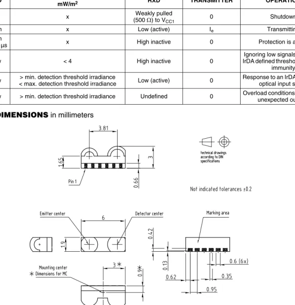
TABLE 2 - TRUTH TABLE
INPUTS OUTPUTS REMARK
SD TXD OPTICAL INPUT IRRADIANCE
mW/m2 RXD TRANSMITTER OPERATION
High
> 1 ms x x
Weakly pulled
(500 ) to VCC1 0 Shutdown
Low High x Low (active) Ie Transmitting
Low > 100 µsHigh x High inactive 0 Protection is active
Low Low < 4 High inactive 0
Ignoring low signals below the IrDA defined threshold for noise
immunity
Low Low < max. detection threshold irradiance> min. detection threshold irradiance Low (active) 0 Response to an IrDA compliant optical input signal Low Low > min. detection threshold irradiance Undefined 0 Overload conditions can cause
unexpected outputs 19612 19728 Emitter Detector 5 x 0.95 = 4.75 0.95 0.64 1 2 3 4 5 6 0.4 1.27 Recommended Footprint Side View Application 19301 Emitter Detector 5 x 0.95 = 4.75 0.95 0.64 1 2 3 4 5 6 0.6 1.27 Recommended Footprint Top View Application
TFBS4711
Serial Infrared Transceiver SIR, 115.2 kbit/s,
2.4 V to 5.5 V Operation
Vishay Semiconductors
REEL DIMENSIONS
in millimeters
TAPE WIDTH (mm) A MAX. (mm) N (mm) W1 MIN. (mm) W2 MAX. (mm) W3 MIN. (mm) W3 MAX. (mm) 16 330 50 16.4 22.4 15.9 19.4 14017
Drawing-No.: 9.800-5090.01-4 Issue: 1; 29.11.05