JOURNAL OF IEEE TRANSACTIONS ON COMPUTERS, VOL. X, NO. X, AUGUST X 1
Polymorphic Accelerators for Deep Neural
Networks
Arash Azizimazreah, and Lizhong Chen,
Senior Member, IEEE
Abstract—Deep neural networks (DNNs) come with many forms, such as convolutional neural networks, multilayer perceptron and recurrent neural networks, to meet diverse needs of machine learning applications. However, existing DNN accelerator designs, when used to execute multiple neural networks, suffer from underutilization of processing elements, heavy feature map traffic, and large area overhead. In this paper, we propose a novel approach,Polymorphic Accelerators, to address the flexibility issue fundamentally. We introduce the abstraction of logical accelerators to decouple the fixed mapping with physical resources. Three procedures are proposed that work collaboratively to reconfigure the accelerator for the current network that is being executed and to enable cross-layer data reuse among logical accelerators. Evaluation results show that the proposed approach achieves significant improvement in data reuse, inference latency and performance, e.g., 1.52x and 1.63x increase in throughput compared with state-of-the-art flexible dataflow approach and resource partitioning approach, respectively. This demonstrates the effectiveness and promise of polymorphic accelerator architecture.
Index Terms—Deep Neural Networks, Accelerators, Configurable Processing Element (PE) Array, PE Array Utilization, Data Reuse.
F
1
I
NTRODUCTIONDeep Neural Networks (DNNs) can achieve unprece-dented accuracy in many machine learning tasks, and have been deployed in many fields [5], [28], [37]. Due to the com-putation and memory intensive nature of DNNs, specialized hardware has been designed for acceleration. Depending on network topologies and structures of layers, different types of DNNs can be formed such as Convolutional Neural Network (CNN), Multilayer Perceptron (MLP), and Recurrent Neural Network (RNN). These models have been widely used in diverse DNN applications (e.g. 95% of inference workloads in Google’s data centers [17], [21]). Thus, it is imperative to design accelerators that can work well with different neural networks.
In a DNN accelerator, a process element (PE) array (e.g., multipliers and adders) performs the actual computation of the network, whereas on-chip buffers store various data such as weights and feature maps. Underutilization of the PE array is a major obstacle for many recent DNN accelerators (e.g. [2], [21], [29], [30], [32], [45]) to achieve high performance. The root cause for the underutilization problem is the mismatch between the static shape of the PE array and the diverse dimensions of layers. This may potentially result in very low utilization especially with compact data types. For instance, the PE array utilization for SqueezeNet in 16-bit fixed-floating point is only around 24% [33].
The main approach to address the underutilization problem is resource partitioning, where each partition is optimized to process a specific set of layers. The coordination of multiple partitions to process a network, however, is a
chal-• A. Azizimazreah was with the School of Electrical Engineering and Computer Science, Oregon State University, USA.
E-mail: [email protected]
• L. Chen is with the School of Electrical Engineering and Computer Science, Oregon State University, USA.
E-mail: [email protected]
Manuscript received mm, dd, yyyy; revised mm, dd, yyyy.
lenging task as complicated dataflows may be needed. Only a few works [2], [12], [20], [33], [40], [44] have achieved this successfully. Nevertheless, existing approaches of resource partitioning suffer from two major issues. First, on-chip and off-chip data traffic is increased considerably. Both on-chip and off-chip data movements are costly in terms of energy consumption, not to mention the large latency of off-chip accesses. Second, existing resource partitioning dataflows cannot process different DNNs efficiently at runtime. This is because those dataflows are optimized for a given DNN at design time, without the ability to dynamically reconfigure the dataflow. Therefore, it is difficult for those schemes to support multiple networks effectively. Alternatively, some works have been proposed to directly reconfigure the acceler-ator, without partitioning/sharing resources among multiple models. Unfortunately, this approach has resulted in hardly acceptable overhead for both ASIC (e.g., 47% more area [22]) and FPGA platforms (more details in Section 3). Thus, it is much needed to develop a fundamentally different way to support multiple neural network models, while reducing data traffic and achieving high PE array utilization.
In this work, we propose a novel Polymorphic
architec-ture, which achieves the runtime reconfigurability of DNN accelerators and enables extensive cross-layer data reuse. The proposed approach is based on a new abstraction that
we introduce calledlogical accelerators. To process different
network layers, multiple logical accelerators can be formed dynamically from a pool of PE cells and memory banks on the physical accelerator. This decoupling allows feature maps to be shared among logical accelerators without physically copying the data. Meanwhile, the flexibility of logical accel-erators provides a way to match better with the diverse layer dimensions across networks. On of top that, we develop three procedures called Polymorph, Feature Map Push and Feature Map Pull, which work collaboratively to orchestrate a sequence of operations to allow variable sizes of logical
accelerators to process multiple layers simultaneously, while increasing the data reuse opportunities. An offline routine is developed to generate parameters that are required by the logical accelerators and associated procedures for any given set of DNNs that need to be accelerated on the hardware. Evaluation results show that the proposed polymorphic architecture is able to reduce off-chip traffic by 25.7% to 77.1% depending on the network. The polymorphic design also increases performance (throughput of inference operations) by 1.52x and 1.63x compared with the state-of-the-art flexible dataflow and resource partitioning approach, respectively, under the same area constraint. The main contributions of this work are the following:
• Proposing a novel concept of logical accelerators to
enable dynamic reconfiguration of DNN accelerators;
• Developing cleverly designed procedures to allow
cross-layer data reuse among logical accelerators;
• Demonstrating the effectiveness of polymorphic
ar-chitecture through extensive evaluation.
The rest of this paper is organized as follows. Section 2 provides more background on DNN accelerators. Section 3 discusses the motivations and challenges of this work. In section 4, we describe the proposed approach in detail. The accelerator implementation methodology is explained in Section 5, and evaluation results and analysis are presented in Section 6. Finally, related work is summarized in Section 7, and Section 8 concludes this paper.
2
B
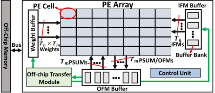
ACKGROUNDTypical DNN accelerators (e.g., [7], [21]) process a DNN in its natural structure, one layer at a time. Generally, a DNN accelerator consists of an array of process element (PE) cells and different on-chip buffers. Fig. 1 presents the datapath of
a typical DNN accelerator. The PE array receivesTn input
feature maps (IFMs) from an input buffer, fetchesTn×Tm
weights from weight buffer, computes Tm output feature
maps (OFMs) and stores the output into an output buffer. If the computation of OFMs needs several iterations, at the beginning of each iteration, a partial sum (PSUM) might be loaded into the output buffer. Then, at the end of each iteration, the PE array writes new PSUMs or final OFMs into the output buffer. A PE cell can be as small as a simple multiplier-and-adder (fine-grained) such as in Google TPUs [21], or as large as a vector-dot-engine (coarse-grained) such as in Microsoft’s BrainWave NPUs [11], [26]. To increase throughput and energy-efficiency, the techniques below are commonly adopted.
Banked On-chip Buffers:Many state-of-the-art accelera-tors on both ASIC and FPGA platforms have large on-chip buffers. For example, Google’s TPU and Xilinx VU13P FPGA have 28MB and 56MB on-chip buffer capacity, respectively [10], [21]. By partitioning a large buffer into smaller banks, high capacitance on long word-lines and bit-lines [42] can be avoided. Furthermore, banked buffers provide more read and write ports. This allows simultaneous accesses to IFMs, weights and OFMs, thus being essential to high-bandwidth data transfer between buffers and PE array.
Tiling: Tiling techniques are often used when feature maps are larger than on-chip buffer banks. A feature map
𝑻𝑻𝒏𝒏 IFMs 𝑻𝑻𝒎𝒎PSUMs 𝑻𝑻𝒎𝒎PSUM/OFMs PE Array W ei gh t Buf fe r 𝑻𝑻𝒏𝒏×𝑻𝑻𝒎𝒎 Weights OFM Buffer IFM Buffer PE Cell Off-chip Transfer Module Control Unit Buffer Bank O ff-C hip Mem ory Bus
Fig. 1. A typical DNN accelerator datapath.
M
𝑩𝑩 𝒄𝒄 𝑩𝑩𝒓𝒓 𝑩𝑩𝒎𝒎R
N
𝑩𝑩𝒏𝒏C
Off-Chip Memory PE ArrayInput Feature Maps Output Feature Maps
Input Buffer
Output Buffer
IFMs Weights PSUM /OFMs PSUM
N=#IFMs, M=#OFMs, R=#Rows, C=#Columns Accelerator’s Core
Bus
Active Bank Inactive Bank
Fig. 2. Tiling and Double Buffering techniques.
is divided into smaller pieces so they can fit into an on-chip buffer bank. Fig. 2 shows an example of tiling for a three dimensional CNN layer, where the unrolling is
determined by tiling factors Bn,Br and Bc. It may take
multiple iterations to load all the IFM tiles that are needed to calculate one OFM tile.
Double Buffering: In order to hide the large off-chip memory access latency, many DNN accelerators (e.g., [2], [3], [21], [22], [29], [32], [33], [39], [45]) adopt a decoupled access/execute architecture [34] to overlap the communica-tion latency of data loading with computacommunica-tion time. This is referred to double buffering. As shown in Fig. 2, during each iteration, the input and output buffers that are being
used by the PE array are calledactiveinput andactiveoutput
buffers (represented as black rectangles), respectively. The other set of buffers are called inactive input and output buffers (represented as white rectangles in Fig. 2). As the
PE array is doing computation on the currentBnIFM tiles,
the inactive input buffer is being used to preload the next
Bn IFM tiles needed for the next iteration. Meanwhile, the
inactive output buffer temporarily keeps the computedBm
OFM tiles from the previous iteration while those tiles are still being written back to off-chip memory. A similar manner is used for weight buffers but are omitted for clarity.
Additionally, in this work, the dimension of a PE array is
defined by a tuple (Tm,Tn)1, whereTmandTnare unrolling
factors of OFMs and IFMs, respectively, as shown in Fig. 1.
3
M
OTIVATION ANDC
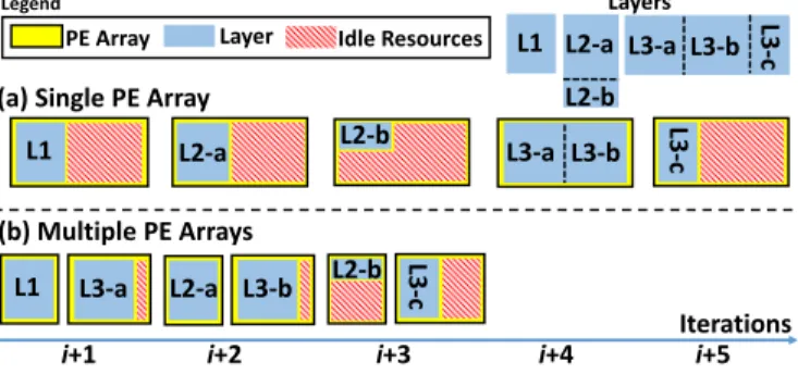
HALLENGES3.1 PE Array Underutilization
A major issue with many recent accelerators (e.g., [21], [29], [30], [32], [45]) is the underutilization of the PE array. Specifically, the dimensions of layers may be different across
1. The PE array shape can be generalized to four dimensions (Tm,Tn, Tr,Tc); the proposed approach is applicable as well.
PE Array Layer Idle Resources Legend L2-a L2-b L1 Layers L3-a L3-b L3-c i+1 i+2 i+3 i+4 i+5
L1 L2-a Layer 2L2-b L3-a L3-b
Iterations (a) Single PE Array
(b) Multiple PE Arrays
L1 L3-a L2-a L3-b
L3
-c
L2-b L3-c
Fig. 3. Underutilization of PE array (a), and the improvement from resource partitioning (b).
a network, but the dimension of the PE array is static in the sense that its numbers of inputs and outputs are fixed after design time. A typical approach is to optimize the PE array shape (dimension) for all the layers as a whole, e.g., Google
TPU uses a systolic array with a fixed dimension (256×256) to
process different deep learning models [21]. However, some underutilization is inevitable [22], [33]. Fig. 3a illustrates an example where a single PE array processes three layers of the same network one by one. Due to the dimension mismatch and fragmentation, the PE array is severely underutilized. it has been shown that, when implemented on a Xilinx Virtex-7 690T FPGA, the overall PE array utilization is Virtex-76.4% for 32-bit floating-point SqueezeNet and less than 24% for 16-bit fixed-point AlexNet [33]. Using more compact data types is equivalent to having larger computational units under a given hardware resource, thus exacerbating the issue. 3.2 Need for Resource Partitioning
To address the PE array underutilization problem, state-of-the-art works have proposed resource partitioning. The basic idea is that, instead of optimizing the PE array dimension for all the layers, hardware resources are divided into multiple coarse-grained partitions. Each partition can be considered as a separate accelerator, and the PE array dimension in each partition is optimized for a subset of layers. Fig. 3b revisits the previous example, but with hardware resources partitioned into two PE arrays with different dimensions to process the three layers – one PE array for layers 1 and 2, and the other for layer 3. It can be seen that the utilization of PE arrays is increased considerably compared with the single PE array case and the overall processing can be completed in fewer number of iterations (5 vs. 3). Note that the layers are still processed in order in Fig. 3b, e.g., the input to layer 3 comes from previous iterations (not shown) where layers 1 and 2 are processed. Thus, the layer processing is done in pipeline.
3.3 Problems in State-of-the-art Designs
Because resource partitioning involves the coordination of multiple partitions, the design of its dataflow can be quite complicated and challenging. To date, only a few works have successfully realized such dataflow [2], [12], [20], [33], [40], [44], but all come with significant inefficiency and limitation. In the design of accelerators, dataflow is a crucial element. It describes the communication patterns between PE cells
and memory resources. In other words, the dataflow defines that, given the datapath of an accelerator such as the one shown in Fig. 1 and Fig. 2, when and where various data (weights, IFMs, PSUMs and OFMs) are transferred between on/off-chip memories and PE cells [24]. For example, in the Weight Stationary (WS) dataflow [7], weights are stored in the local buffers of PE cells. The weights are “stationary” in the sense that the same weights are reused multiple times, while different IFMs are loaded and processed from off-chip memory. In contrast, in the Output Stationary (OS) dataflow [7], PSUMs are stationary in the local buffers of PE cells and reused multiple times for different IFMs and weights.
There are two key issues that remain to be addressed in existing works. First, both off-chip and on-chip traffic are greatly increased. Resource partitioning in general creates more off-chip traffic, as IFMs to a partition are reused only by the PE cells in that partition but not the PE cells in other partitions. Also, the on-chip buffer allocated to each partition is smaller, which leads to more off-chip traffic (analogous to smaller cache size for the same working set). Our experiments have shown that, for a simple AlexNet with five CNN layers, resource partitioning increases the off-chip feature map traffic by 20.3%. The situation becomes worse for deeper models. For example, this percentage increases to 30.6% for SqueezeNet with 26 layers (2 CNN layers, plus 8 fire modules each having 3 layers). Some existing works try to mitigate this issue by forwarding data from the output buffer of the current partition to the input buffer of the next partition (inter-layer reuse [2], [12]). While these works can reduce the off-chip traffic, a significant portion of the off-chip traffic still remains, and the on-chip traffic is increased due to data forwarding. It is worth noting that both off-chip and on-chip traffic are very costly. Prior research has revealed that a 32-bit floating-point addition needs only 1pJ, whereas getting access to a 32-bit word in DRAM consumes 640pJ and performing a single pair of 32-bit on-chip reading and writing consumes 100pJ in 45nm CMOS technology [15], [19]. Therefore, it is important to reduce data traffic in accelerators to increase the efficiency.
Second, existing resource partitioning dataflows can-not support different neural network models efficiently at runtime. Previously proposed dataflows for resource partitioning can be optimized for a given model at design time, but they do not have the flexibility to reconfigure dynamically [12], [44]. This reconfigurability is critical to efficiency. We have characterized several mainstream deep learning models using the average operational density, and observed that it can vary by hundreds to thousands of times among the models, e.g., from 1 operation/byte in MLP, to 50 in LSTM, to 8,754 in AlexNet. This is because CNN models (e.g., AlexNet) are computation-intensive, thus performing more operations per data (e.g., feature maps and/or weights) than memory-intensive MLP and LSTM models. It is, thus, critical to design dataflow accordingly. For example, consider an LSTM or MLP model in real-time AI applications where no batching is available. The Weight Stationary dataflow would perform poorly as there is little opportunity for weight reuse. Instead, a dataflow based on reusing outputs or PSUMs would be more appropriate. Therefore, in order to run multiple neural network models efficiently on an accelerator, flexible dataflow is needed to match with different models,
which may be processed simultaneously across partitions. This means an approach is needed where while it provides partitioning for parallel processing, each partition can be dynamically reconfigured during run-time to match with layer requirements in different networks. Unfortunately, none of the current resource partitioning approaches provides such flexibility.
3.4 High Cost in Reconfigurable Platforms
In addition to resource partitioning, another approach to increase PE array utilization is to directly reconfigure the dataflow to match with the current model that is being executed (without partitioning/sharing resources among multiple models). This has been achieved on both AISC and FPGA platforms, albeit at very high costs.
The latest and best approach so far on realizing re-configurable ASIC DNN accelerators is via rere-configurable interconnects [22]. It indeed allows the use of different dataflows to process different deep learning models. How-ever, the approach relies on a complex network-on-chip (NoC) architecture to connect various adders, multipliers
and local buffers together. In some sense, this approachshifts
the challenging task of providing reconfigurable accelerators to the NoC designs, rather than proposing a fundamental solution to achieve reconfigurability. This leads to a dramatic overhead for the interconnects and accelerator, with 47% more area than the baseline design with a systolic PE array [22].
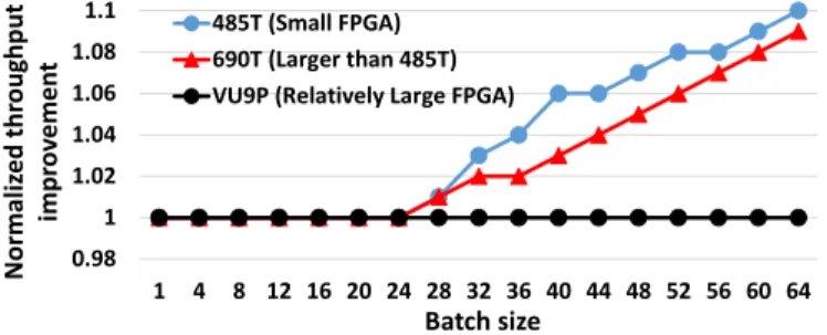
Meanwhile, FPGAs are often used for machine learning acceleration as a reconfigurable platform. Although the prevalent belief is that they can be reconfigured for each layer or a subset of layers for higher performance, the reconfiguration overhead can be so high that it might not be productive in terms of net performance improvement. Fig. 4 shows one of our interesting experiments on the throughput improvement of SqueezeNet, when three Xilinx FPGAs are used for reconfiguration. In this experiment, for each layer if a new configuration leads to an overall performance improvement by considering the reconfiguration latency overhead, the new configuration is issued; otherwise the system continues with its current configuration. As can be seen, if the batch size is less than 24, regardless of the FPGA size, no reconfiguration is issued because there is no net performance benefit. For smaller FPGAs (485T and 690T), they have fewer number of DSP slices and require a smaller bit-stream (reconfiguration data) to be loaded into the reconfiguration memory of FPGA. Hence, the reconfiguration overhead is easier to be amortized by increasing the batch size. For the large VU9P FPGA, the breakeven point is not reached even when the batch size is 64. The large reconfiguration overhead of FPGA makes it a less attractive option, especially for cases where batch sizes are small, e.g., real-time AI (batch size is 1) [11].
3.5 Challenges
From the above discussions, it is evident that a new approach is much needed that can provide flexible configurations for different neural network models while reusing data efficiently in resource partitioning. This section analyzes
0.98 1 1.02 1.04 1.06 1.08 1.1 1 4 8 12 16 20 24 28 32 36 40 44 48 52 56 60 64 485T (Small FPGA) 690T (Larger than 485T) VU9P (Relatively Large FPGA)
N or m al ize d t hr oug hp ut imp ro ve me nt Batch size
Fig. 4. Normalized throughput improvement when reconfiguration is used for SqueezeNet.
major limiting factors and challenges to realize such an approach.
Dynamic Reconfiguration: While sounds exciting,
achieving efficient reconfiguration in terms of PE array dimensions, buffer shapes, dataflow and partition sizes is a difficult task for several reasons. First, in existing partitioning approaches, resources are allocated physically to partitions at design time. In order to provide the flexi-bility in allocation, we need a way to decouple partitions from physical resources. Second, as the resources of each partition are changing dynamically, some method is needed to efficiently track and update partition information during runtime and, more importantly, enforce the partitioning in the hardware physically. Third, the shapes of the PE array and buffers in a partition need to match with the requirement of network layers. This demands coordination of resources and data distribution within and across partitions. Finally, the reconfiguration scheme needs to have good extensibility that can support new DNN models even after the accelerator has been implemented.
Data Reuse and Sharing: To reduce off-chip traffic, feature map data should be shared and reused among partitions as much as possible. The challenge, however, lies in two aspects. First, it is challenging to store the forwarded reusable data without using additional buffers. These data might take several iterations to consume. This requires careful coordination between partitions to somehow use existing buffers to store the data without compromising the original functionality of input/output and active/inactive buffers. Second, for feature map data that can be shared, it is still costly to copy data between partitions, even on-chip. Therefore, we need a more efficient way to share the data without actually copying data between the buffers of PE cells.
4
P
ROPOSEDA
PPROACH4.1 Basic Idea
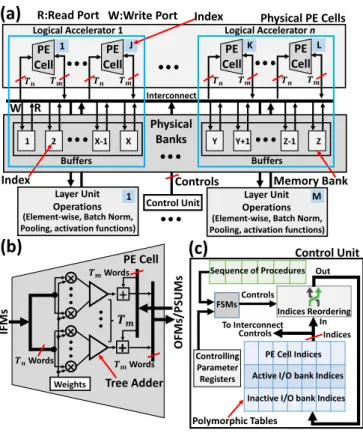
To address the above issues, we proposePolymorphic
accel-erators, a novel approach to achieve the reconfigurability that is needed to efficiently execute diverse neural networks on the same accelerator. To achieve that, we introduce the
abstraction ofLogical Accelerators, which can be constructed
dynamically from a pool of physical PE cells and memory banks to match different layer dimensions in a network, as shown in Fig. 5. Specifically, for each of the neural networks that needs to be accelerated, an offline software routine is run
Layer Unit Operations
(Element-wise, Batch Norm, Pooling, activation functions)
(a)
Logical Accelerator 1 PE Cell 𝑻𝑻𝒏𝒏 𝑻𝑻𝒎𝒎 R W Interconnect 1 2 X-1 X Y Y+1 Z-1 Z Buffers Buffers Layer Unit Operations(Element-wise, Batch Norm, Pooling, activation functions)
PE Cell 𝑻𝑻𝒏𝒏 𝑻𝑻𝒎𝒎 PE Cell 𝑻𝑻𝒏𝒏 𝑻𝑻𝒎𝒎 PE Cell 𝑻𝑻𝒏𝒏 𝑻𝑻𝒎𝒎 Physical PE Cells Logical Accelerator n 1 J K L Index 1 M × × × ×
+
+
𝑻𝑻𝒏𝒏Words 𝑻𝑻𝒎𝒎Words Weights PE Cell IFMs Tree Adder 𝑻𝑻𝒎𝒎Words O FMs/ PS U Ms 𝑻𝑻𝒎𝒎 Control Unit(b)
Physical BanksIndex Memory Bank
W:Write Port R:Read Port
(c)
Indices Reordering
PE Cell Indices Active I/O bank Indices Inactive I/O bank Indices Controlling Parameter Registers Indices To Interconnect FSMs Sequence of Procedures Controls In Out Polymorphic Tables Control Unit Controls Controls
Fig. 5. Proposed polymorphic approach.
once to generate the best configuration for the network (e.g., the optimal number of logical accelerators, the dimension of each logical accelerator, and other parameters that are needed at runtime). The configurations, one for each network, are passed on and stored in a control unit in hardware. During runtime reconfiguration (i.e., when the accelerator needs to execute a particular neural network), the control unit simply loads the corresponding configuration and enforces the configuration in hardware. The enforcement (i.e., reconfiguration) is achieved by maintaining and updating a polymorphic table (Fig. 5c) for each logical accelerator that stores the indices of the constituent physical PE cells and memory banks.
The core of the polymorphic design is three procedures, namely Polymorph, feature map Push (FM Push), and feature map Pull (FM Pull), that work together to orchestrate a sequence of operations to allow variable sizes of logical accelerators to process multiple layers simultaneously, while maximizing the opportunity for cross-layer data reuse among the logical accelerators.
In a nutshell, the proposed accelerator is made
poly-morphic by (1) having an offline routine to generate the
needed configuration for each neural network, and (2) augmenting components in the accelerator to switch to
(and enforce) any particular configurationonline. Note that
this reconfiguration is fundamentally different from using a reconfigurable platform (e.g., FPGA). In the FPGA case, the accelerator needs to be re-compiled if accelerating a different neural network, thus being slow. In contrast, the proposed polymorphic accelerator has fixed hardware after manufacturing, but still be able to reconfigure by loading and enforcing different configurations, thus being fast and
LA2 LA1 Group 1 PE Index=2 PE Index=3 In out In Out Active 10 11, 12 16 17, 18 Inactive 7 8, 9 13 14, 15 Group 1 PE Index=1 In out Active 4 5, 6 Inactive 1 2, 3 1 4 5 𝟐𝟐 1 1 𝟐𝟐 1 𝟐𝟐 PE
Cell 1 PE Cell 2 PE Cell 3
Physical PE Cells Physical Banks R W 2 3 6 7 8 9 10 11 1213 141516 17 18 Active data Inactive data Polymorphic Table Polymorphic Table
LA: Logical Accelerator
W: Write Port R: Read Port
Fig. 6. Multiple logical accelerators can be defined on the hardware by using polymorphic tables.
requiring no compiler support.
In the remainder of this section, we present the details of the polymorphic architecture, the three runtime procedures, the offline routine, the interconnect structure, and how the design can be easily extended to support new networks that need to be accelerated.
4.2 Logical Accelerators
The key element in the proposed polymorphic accelerator
architecture islogical accelerators. A logical accelerator consists
of one or multiple groups of hardware resources, where each group contains a subset of physical PE cells and physical memory banks (hereafter, unless otherwise stated, PE cells and memory banks mean the actual physical resources). Dur-ing runtime, logical accelerators are constructed dynamically. Each logical accelerator is assigned to process a layer. Thus, multiple logical accelerators can process multiple layers simultaneously.
Fig. 6 illustrates an example where two logical accelera-tors are formed from a subset of the PE cells and memory
banks. Each logical accelerator has a polymorphic table in
the control unit in Fig. 5c that defines the configuration of the logical accelerator. A group in an logical accelerator is defined by one row in the polymorphic table which contains the indices of PE cells and memory banks. For instance, consider the second logical accelerator (LA2 in green). The logic PE array of LA2 consists of PE cell 2 and PE cell 3. Each PE cell has its own four types of logic buffers (i.e. active input, inactive input, active output, and inactive output) and the indices of the physical memory banks for each logic buffer are stored in the polymorphic table. In this example, LA2 has only one group, but in general, a logical accelerator that processes a layer might have several groups and thus several rows in the polymorphic table.
Logical accelerators can be reconfigured during runtime by updating the indices in the polymorphic tables. Specifi-cally, during a given round (e.g., an iteration or a cycle), the finite state machines (FSMs) in the control unit calculate the updated indices of the polymorphic tables for the next round. Those indices determine which PE cells should be physically connected to which memory banks during the next round. This is implemented by setting the interconnect accordingly (e.g., crosspoints in the crossbar) by the control unit at the beginning of the next round to reflect the new configuration. Besides the flexibility in forming logical accelerators that can match better with the shapes of the layers, the abstraction
𝑻𝑻𝑵𝑵 𝑻𝑻𝑴𝑴 PE Cell PE Cell 𝒑𝒑=𝑵𝑵𝑷𝑷𝑷𝑷 𝑻𝑻𝑹𝑹 𝑻𝑻𝑹𝑹 (a) (b) 𝑻𝑻𝒏𝒏 𝑻𝑻𝒏𝒏 𝑻𝑻𝒎𝒎 𝑻𝑻𝒎𝒎 𝒑𝒑
Fig. 7. Configurable PE array.
of logical accelerators also allows data to be reused more efficiently. By exchanging indices in the polymorphic tables, reusable data can be fed to another logical accelerator without physically copying the data between memory banks. Those advantages and properties provide the basis for our proposed Polymorph, FM Push and FM Pull procedures.
4.3 Polymorph Procedure
The Polymorph procedure consists of a cleverly designed sequence of steps that operate a set of small PE cells as if there is only one large (logical) PE cell. Precisely, given a total
number ofNP EPE cells each with dimension (Tm,Tn), they
can be divided intoTRnumber of groups. As illustrated in
Fig. 7a, a large logical PE cell with dimension (TM,TN) can
be formed by groupingpPE cells, where
p=NP E/TR, TM =p×Tm, TN =p×Tn
The resultingTRlarge logical PE cells operate in parallel
to process a layer. This creates a 3-D shape vector-dot-engine (a logical PE array), which receives an input window of
TR×TN IFMs and computes an output window ofTR×TM
OFMs as shown in Fig. 7b. By changingTR, the size of the
input and output processing windows can be adjusted to match with the layer dimensions in different networks to increase PE cell utilization. The main challenge, however, is how to orchestrate individual fine-grained PE cells to distribute and share data efficiently. For example, by the
definition of convolution, each of theTN IFMs of the large
logical cells needs to be multiplied by the weights in each of its constituent small PE cells, so each PE cell cannot simply
processTnIFMs and discard them.
The Polymorph procedure executes two steps repeatedly
to achieve the above objective:Reuse-Compute/Preload(RCP)
andRotate. In the RCP step, the IFMs in the active input buffers are first reused. Then, while the PE cells are comput-ing the OFMs/PSUMs, the next tiles of IFMs are preloaded
into the inactive input buffers. In theRotatestep, the indices
of the memory banks in the active input buffers of a group are rotated. This allows IFMs to be shared among the PE
cells. TheRCPandRotatesteps are repeatedptimes in total
to maximize data reuse and make time for the next iteration of IFMs to be fully preloaded.
Fig. 8 demonstrates how the Polymorph procedure is executed to construct a logical accelerator with a shape of
(TM, TN), using one group of p PE cells where each PE
cell hasTnIFM inputs andTmOFM outputs. If the logical
accelerator has more than one group, a similar execution flow is used for other groups. In this example, the logical
accelerator needs to process a layer with2×p×Tn IFMs
andp×TmOFMs. Each small vertical rectangle represents a
memory bank. The buffers closer to the PE cells are the active buffers, and the inactive buffers are beneath the active ones. If each bank stores one feature map, in one IFM iteration, the
logical accelerator can readp×TnIFMs and computep×Tm
OFMs. Therefore, two IFM iterations are needed to load all
the2×p×TnIFMs required to compute allp×TmOFMs.
Each IFM iteration needs to execute theRCPandRotatesteps
ptimes, as explained below.
Fig. 8-Label1 shows the status of each bank and PE cell
at the beginning of the Polymorph procedure. The active
input buffers are labeled by ”I1” to ”Ip”, and they contain
IFMs (indicated by the blue rectangles) which can be used
to perform the first round ofRCP. These IFMs are reusable
data brought into the active input buffers by the FM Pull procedure in the previous iteration (explained in the next subsection). Thus, for the first IFM iteration, no IFM needs to be actually loaded from off-chip.
The first IFM iteration starts by the first round of RCP
step as shown in Label2. The PE cells are highlighted in
yellow to show that they have started the computation to calculate the PSUMs in the active output buffers (represented by the yellow rectangles). While the PE cells are performing the computation, the first tile of the IFMs required for the next (second) IFM iteration is preloaded from off-chip into an inactive input buffer as indicated by the red rectangles and red arrow. After finishing the computation, as shown
in Label3, theRotatestep is executed to rotate the memory
banks among the active input buffers in order to reuse the on-chip IFMs among PE cells, i.e., the old I1 becomes the new I2, old I2 becomes new I3, and so on. After executing theRotatestep, in Label4, another round of computation is performed by the PE cells to calculate their OFMs with new IFMs after rotation. Again, while the PE cells are calculating, the next tile of IFMs required for the second IFM iteration are preloaded into the inactive input buffers.
The process of executing the RCP and Rotate steps
continues for anotherp−2rounds in order to reuse and
process all the on-chip IFMs in the active input buffers. At this time, the first IFM iteration of OFM computation is completed. More importantly, the inactive input buffers have been preloaded with the IFMs needed by the second IFM iteration. To use these data, the bank indices of the active input buffers are exchanged with the bank indices of the
inactive input buffers. Then, theRCPandRotatesteps are
executed for another p rounds to finish the computation
for the second IFM iteration and consequently for OFMs as shown in Fig. 8. In the final state in the figure, all the IFMs in the active input buffers are consumed by the PE cells and marked as empty banks, represented as the white rectangles. The computed OFMs are stored in the active output buffers
as indicated by the black rectangles2. As mentioned earlier,
the rotates and exchanges are done through updating the indices in polymorphic tables, not copying data physically between memory banks, thus reducing both off-chip and on-chip memory operations.
How to group several PEs together PE Cell 𝑻𝑻𝒎𝒎 𝑻𝑻𝒏𝒏 I1 Out In . PE Cell Ip Out In PE Cell I2 Out In PE Cell 𝑻𝑻𝒎𝒎 𝑻𝑻𝒏𝒏 I1 . PE Cell Ip PE Cell I2 Off-Chip Memory PE Cell 𝑻𝑻𝒎𝒎 𝑻𝑻𝒏𝒏 I1 . PE Cell Ip PE Cell I2 Group PE Cell Ip-1 . PE Cell 𝑻𝑻 𝒎𝒎 𝑻𝑻𝒏𝒏 Ip PE Cell I1 Group Off-Chip Memory 1 2 3 4
p-2 Rounds of Rotateand RCP PE Cell Ip-1 . PE Cell 𝑻𝑻 𝒎𝒎 𝑻𝑻𝒏𝒏 Ip PE Cell I1 Group Final
Inactive & Empty
Active & Empty Active & Contain IFM
Bank Status
Active & Contain PSUM Active & Contain OFM Inactive & Contain Pre-loaded IFM
Group Group
pRounds of Rotate and RCP
First IFM Iteration Second IFM Iteration
Exchange active input with inactive input
Fig. 8. Illustration of the Polymorph procedure for a group to build a logical PE array and process a layer.
PE Cell 𝑻𝑻𝒎𝒎 𝑻𝑻𝒏𝒏 PE Cell 1
(a)
𝑻𝑻𝒎𝒎 𝑻𝑻𝒏𝒏 PE Cell 𝑻𝑻𝒎𝒎 𝑻𝑻𝒏𝒏 PE Cell 2 𝑻𝑻𝒎𝒎 𝑻𝑻𝒏𝒏 LA: Logical Accelerator Inactive & EmptyActive & Empty Active & Contain IFM
Bank Status
Active & Contain OFM
Inactive & Contain Pre-loaded IFM Inactive & Contain reusable IFM
PE Cell
𝑻𝑻𝒎𝒎
𝑻𝑻𝒏𝒏 PE Cell 𝑻𝑻𝒏𝒏 PE Cell 𝑻𝑻𝒎𝒎 PE Cell
PE Cell
𝑻𝑻𝒎𝒎 PE Cell Off- 𝑻𝑻𝒏𝒏 PE Cell 𝑻𝑻𝒎𝒎 PE Cell
Chi p Mem or y 1 2 PE Cell 𝑻𝑻 𝒎𝒎 PE Cell PE Cell 𝑻𝑻 𝒎𝒎 𝑻𝑻𝒏𝒏 PE Cell FM Pull is running
(b)
𝑻𝑻𝒏𝒏 Final 𝑻𝑻𝒎𝒎 𝑻𝑻𝒏𝒏 𝑻𝑻𝒎𝒎 𝑻𝑻𝒏𝒏 𝑻𝑻𝒎𝒎 𝑻𝑻𝒏𝒏 𝑻𝑻𝒏𝒏 𝑻𝑻𝒏𝒏 𝑻𝑻𝒎𝒎 𝑻𝑻𝒎𝒎 𝑻𝑻𝒏𝒏 𝑻𝑻𝒎𝒎 𝑻𝑻𝒏𝒏FM Push is running FM Pull is running FM Push is running LA i-1 LA i-1 LA i-1 LA i LA i LA i LA i LA i Off-Chip Memory
Fig. 9. (a) Feature Map Pull procedure, and (b) Feature Map Push procedure.
4.4 Feature Map Push and Pull Procedures
The Feature Map Push and Pull procedures initialize logical accelerators and enable cross-layer feature map reuse.
Feature Map Pull(or Pull procedure for short) has two main functions: (1) initialize the polymorphic table, and (2) prepare IFMs for the Polymorph procedure by loading from off-chip or reusing on-chip. The first function is achieved straightforwardly by initializing the polymorphic table using the FSM in the control unit. As discussed, for each layer,
TRdetermines the number of groups in a logical accelerator.
The FSM creates TR rows in the polymorphic table, one
row for each group. The format of each row is shown in Fig. 6. For every execution of the Pull procedure, the rows are initialized with indices of the corresponding PE cells and memory banks.
For the second function, depending on which layer is being processed, there are two cases. In the first case, this is the first layer of the network assigned to the logical accelerator. The Pull procedure has to load the IFMs from off-chip memory since there is no cross-layer feature map
reuse opportunity for the first layer. Fig. 9a illustrates the execution of the Pull procedure for this case. As shown in
Fig. 9a-Label1, the off-chip IFMs are loaded into the inactive
input buffers and then exchanged with the active input buffers (through indices exchange, not copying physically)
as denoted by the bidirectional red arrow. Label2 shows the
final state after the Pull procedure execution. The active input buffers contain IFMs (blue rectangles) which can be used for the layer computation. This final state has the same format as
the initial state of the Polymorph procedure in Fig. 8-Label1.
Thus, the Polymorph procedure can be started immediately after the Pull procedure. In the second case, this is not the first layer, so the IFMs can be obtained from the Feature Map
Push procedure of thepreviouslayer (logical accelerator), as
described below.
Feature Map Push (or Push procedure) works in pair
with the Pull procedure. The main objective is to reuse the computed OFMs as IFMs between two logical accelerators. For a clear explanation of how the Push procedure works, consider two logical accelerators, where one is assigned to
process layeri-1 and the other is assigned to process layer
i. Therefore, for each input data, the computed OFMs of
logical acceleratori-1 can be reused as the IFMs for logical
acceleratori. This requires the Push procedure to be run on
logical acceleratori-1to “push” feature map data to logical
acceleratoriwhere the Pull procedure runs on to “pull” the
data into the input buffers. Again, all the data exchange is through manipulating indices in polymorphic tables.
Fig. 9b shows how the two procedures work together. As
shown in Label1, feature map forwarding is realized by
exchanging memory banks in the active output buffers of
LAi-1 (which contains computed OFMs indicated by the
black rectangles) with memory banks in the active input
buffers of LAi. However, it is possible that the number of
banks in the active output buffers of LAi-1 is larger than
the number of banks in the active input buffers of LAi. To
reuse the remaining computed OFMs, note that the inactive
input and output buffers of LAimust be empty by now. This
is because LAihas already processed all the IFMs in the
previous iteration and is running the Pull procedure to get
more data. Consequently, the remaining OFMs from LAi-1
are forwarded to the inactive buffers of LAithrough bank
index change, as shown in Label2. In case that some OFMs
still remains after using the inactive buffers of LAi, those
OFMs are written back to off-chip memory for future uses,
as shown in the red arrow to off-chip memory in Label 2.
The final outcome after executing the Push and Pull
procedures is also shown in Fig. 9b. For LAi-1, the active
output buffers are marked as empty (white rectangles) as
the computed OFMs have been forwarded to LA i. Note
that, this might not be the final state of LAi-1, as its active
and inactive input buffers might be loaded with reusable
data from LAi-2, through the Push-Pull procedures between
LA i-2 and LAi-1. For LAi, this is indeed the final state
where reusable IFMs are loaded into the active input buffers (blue rectangles) and potentially the inactive buffers (striped blue rectangles). After this, the Polymorph procedure of LA
ican start immediately. With reusable IFMs in the inactive
buffers, the off-chip preloading operations in the Polymorph procedure (red arrows in Fig. 8) do not happen until the IFMs in the corresponding inactive buffers are consumed first. 4.5 Simultaneous Layer Processing
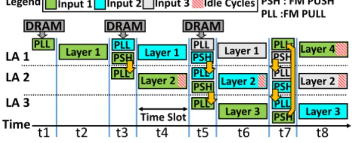
Fig. 10a illustrates how the proposed polymorphic accelerator uses the above three procedures to process a network. Without loss of generality, three logical accelerators (LA1, LA2, and LA3) are created to process a network for three segments of input data, represented as different colors. At time slot t1, LA1 runs the Pull procedure (“PLL” in the figure) to initialize the polymorphic table and load the IFMs of the first layer from off-chip memory. At t2, LA1 runs the Polymorph procedure to form the PE array and its buffers to process the first layer. At the end of layer processing at t3, the Push procedure of LA1 (“PSH” in the figure) and the Pull procedure of LA2 work as a pair to initialize the polymorphic table of LA2 as well as reuse the computed OFMs of LA1 as the IFMs of LA2 for the second layer processing. At the same time at t3, the Pull procedure of LA1 is executed to update the polymorphic table and read the IFMs for the second input data segment from off-chip memory (teal color). At t4,
Layer 1 PSHPLL LA 1 LA 2 LA 3 PLL DRAM PLL DRAM Layer 2 Layer 1 PSHPLL DRAM PLL PSH PLL Layer 3 PSH Layer 2 Layer 1 PSHPLL PLL PSH PLL Layer 4 Layer 2 Layer 3
Time Time Slot
Input 1 Input 2 Input 3 Idle Cycles
PLL :FM PULL PSH : FM PUSH Legend
t1 t2 t3 t4 t5 t6 t7 t8
Fig. 10. Simultaneous processing of network layers.
both LA1 and AL2 run the Polymorph procedure to process their corresponding data simultaneously. A similar pipelined manner is followed to process other layers, e.g., at t7, three pairs of Push-Pull are running to reuse cross-layer data.
Additionally, a logical accelerator is always used to process the same layer but with different inputs consecutively, e.g. LA1 is used to process layer 1 from t1 to t7. Thus, the same weights on the LA can be reused for different inputs. 4.6 Interconnects
Interconnects are used to support the communication for PE cells to read IFMs and PSUMs and write OFMs/PSUMs to/from buffers. As an example, consider implementing the Polymorphic accelerator on the Xilinx Virtex-7 FPGA. One good implementation, based on the offline routine that is described in the next section, needs 14 PE cells, each having a
size of (Tm=17, Tn=3), and 560 memory banks. This translates
into having interconnect networks of size14×560between
PE cells and memory banks, and no interconnect is needed between PE cells or between memory banks based on Fig. 5a. The cost of such an interconnect network is very reasonable, accounting for less than 10% of the power and area of the accelerators.
This overhead is significantly less than existing config-urable accelerator works (e.g., 47% additional area for the interconnects in [22] over the baseline design with systolic PE array). The main reason is that, those works need to use complex interconnects to support reconfigurability. For example, MAERI (a recent work) uses three configurable interconnects, one for the distribution of weights and IFMs among multipliers, one for the forwarding of IFMs between multipliers, and one for the reduction of partial results. This unnecessarily complicates the interconnect designs. However, the interconnect in the Polymorphic accelerator simply performs the function of the interconnect itself – connecting PE cells to memory banks. Thus, a simple crossbar may suffice. The connectivity at each crosspoint is set based on the configuration for a given neural network.
5
I
MPLEMENTATIONM
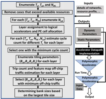
ETHODOLOGYAs mentioned previously, we develop an offline routine to generate optimized configurations for different neural networks. Fig.11 illustrates the flow chart of this routine. The inputs to the routine include the layer details of the networks, resource profile of the FPGA or specification of the ASIC chip, data type format, overhead constraints, and maximum memory bandwidth. The outputs of the offline
routine include two types of parameters. The first type is
static parameters such as the PE cell dimensions (Tm,Tn)
and total number of PE cells (NP E). These static parameters
are used to build the accelerator’s datapath (e.g., in HDL or HLS codes) during implementation. The second type is dynamic parameters. They act as input arguments for the three procedures and provide required information such as
the number of logical accelerators (NLA), tiling parameters
for each layer, and number of rows in polymorphic tables
(TR) for each layer. The routine considers the impact of
parameters on cycle count and off-chip traffic in two phases, respectively.
The routine starts by enumerating all possible
combina-tions for (Tn, Tm, NP E), and removes the ones that exceeds
the available hardware resources of the platform (e.g., LUT counts, number of I/O ports, memory). For each viable
combination of (Tn, Tm, NP E), the routine enumerates the
number of logical acceleratorsNLA. Then, network layers are
assigned toNLAlogical accelerators in a way that adjacent
layers are assigned to consecutive logical accelerators as explained in Section 4.5. For each layer, the number of operations (additions and multiplications) is estimated based on the number of output neurons and layer type, from which the number of PE cells allocated to each logical accelerator can be calculated (i.e., proportional in order to balance pipeline). Finally, using the expressions introduced in prior work [30], [33], [45], the cycle count for each logical accelerator during a layer processing can be estimated by:
cycle count=dM TMe × d N TNe × d R TRe ×C×K×K×p
whereM,N,R, andCare layer dimensions shown in Fig.2,
andTM,TN,TR, andpare PE array dimensions and number
of PE cell in each group, respectively, shown in Fig.7. The
routine selects (Tn, Tm, NP E, NLA) andTRthat leads to the
minimum cycle count.
The second phase considers feature map off-chip traffic. For a logical accelerator, there are four tiling parameters
(Bm, Bn, Br, Bc) shown in Fig. 2 which define tile sizes
and consequently buffer sizes and off-chip traffic. The tiling parameters can be different for each layer. The routine
enumerates the combination of (Bm, Bn, Br, Bc) and uses
the equation below to select the one that leads to the minimum off-chip traffic while not exceeding the available on-chip memory:
#of f chip accesses=γI n×T ileI n+γO ut×T ileO ut
whereT ileiis tile size andγiis the trip count for buffers. Trip
count refers to the number of times that a buffer is loaded or stored from/into off-chip memory. It can be estimated using a simple function that consists of four nested loops (one loop for each layer dimension). The function counts the number of times that buffers are loaded or stored for a given combination of tiling parameters during layer processing by considering the Push and Pull procedures.
Due to the limited ranges of parameters, the above routine is fast despite having several enumeration operations, and usually completes under a minute. Note that having an offline “helper” program has been commonly used in recent accelerator works [12], [16], [22], [44], although the specific functionality of the routine is different in this work.
Extensibility is another advantage of the proposed ap-proach. If a new network needs to be executed on the
Enumerate Tn, Tm, and NPE
For each (Tn, Tm, NPE) enumerate NLA
Remove cases that exceed available resources
Select one with the minimum cycle count For each (Tn, Tm, NPE,NLA) estimate cycle
count for different Trfor each layer
Layer assignment to logical accelerators and PE cell allocation
Enumerate tiling parameters (Bm,Bn,Br,Bc) for each layer
Trip count and feature map off-chip traffic estimation for each layer Select (Bm,Bn,Br,Bc) for each layer
with minimum off-chip traffic Determining bank sizes based
on the largest tile size
Static Parameters Dynamic Parameters Accelerator Datapath Implementation Polymorphic Accelerator Run Time Input Data Output details of networks, resource profile, … Inputs Outputs Polymorphic Accelerator
Fig. 11. Routine for generating parameters.
accelerator, the routine is run on the host CPU to generate the needed parameters for the new network. The host CPU then updates the control unit in the accelerator with these dynamic parameters, which are used to initialize logical accelerators when the new network is executed.
For implementation, we use FPGA as the evaluation platform to demonstrate the effectiveness of the proposed polymorphic approach. This allows us to assess the design under different settings, and follow the transactions between the accelerator’s core and off-chip memory precisely. We model the accelerator using HLS (high-level-synthesis) in Xilinx Vivado HLS. The implementation is parametrized, and the parameters can be set to the optimal values generated by the offline routine. Although the evaluation is conducted using FPGA, a similar flow can be used to implement the polymorphic architecture on ASIC. As mentioned earlier, the reconfigurability of the proposed polymorphic accelerator is not from the platform but rather from the architecture itself.
6
R
ESULTS ANDA
NALYSISWe first compare the polymorphic (PM) architecture with a baseline (BL) design in accelerating 7 neural networks to illustrate various aspects of PM in detail. We then evaluate against several state-of-the-art designs to highlight the advantages of PM. Finally, the scalability of PM and the impact of using compact data types are presented.
6.1 Evaluation of Polymorphic Architecture
The evaluation in this section is carried out on Xilinx Virtex UltraScale+ VU9P FPGA using 32-bit floating-point at 200MHz. The baseline is modeled after Section 2 that includes banked buffers, tiling, and double buffing, and has fixed PE array dimensions. To make the baseline more competitive, we also augment it by implementing functional units that perform operations such as pooling and activation function in a pipelined fashion, so as to overlap their operations
TABLE 1
Baseline (BL) vs. Polymorphic (PM)
Deep Learning Model Type Irregular CNN Regular CNN Inception CNN Residual CNN RNN Fully Connected
Network AlexNet SqueezeNet VGGNet-D GoogLeNet ResNet-34 LSTM MLP
Approach BL PM BL PM BL PM BL PM BL PM BL PM BL PM DSP Usage 98% 98% 98% 98% 98% 98% 99% 98% 99% 98% 96% 95% 98% 99% BRAM Usage 99% 98% 94% 98% 96% 97% 92% 91% 96% 86% 32% 31% 32% 29% Latency (ms) 6.24 2.62 4.01 2.15 56.75 51.03 8.53 6.76 15.62 13.38 0.15 0.12 0.001 0.0009 Off-chip FM traffic (MB) 46.0 22.3 46.0 27.5 101 30.2 53.0 12.1 69.0 9.94 4.21 3.13 0.03 0.02 Throughput (GOPS) 214.6 510.6 280.0 523.1 479.8 533.5 416.6 525.5 455.2 531.4 423.6 512.5 350.7 467.7 TABLE 2
Resource Partition (RP) vs. Polymorphic (PM)
Approach RP [33] PM
FPGA Virtex-7 690T Virtex-7 690T
Frequency(MHz) 100 100
Network AlexNet AlexNet
Data Format (Floating-point) 32-bit 32-bit
DSP Usage 88% 89%
BRAM Usage 49% 37%
On-Chip Power (Watts) 10.2 11.3 Off-chip FMs (MB) 52.8 32.7 Throughput(GOPS) 113.9 127.7
TABLE 3
Performance Comparison with state-of-the-art single-layer accelerator on equivalent FPGAs Approach Design in [25] PM FPGA Arria-10 GX 1150 Virtex-7 485T Frequency(MHz) 150 150
Network VGGNet-D VGGNet-D Data Format (Fixed-point) 16-bit 16-bit
DSP Usage 100% 100%
BRAM Usage 70% 89%
Latency (ms) 47.97 41.32
On-Chip Power (Watts) 21.2 17.5 Off-chip FMs Traffic (MB) Not Reported 32.6 Throughput(GOPS) 645.3 809.0
with PE array computation. The offline routine described in the previous section is used to generate optimal parameters such as PE array dimensions and buffer size for the baseline design. In other words, the baseline design can be considered as a special case of polymorphic design where it has only one logical accelerator with one PE cell and one group.
Consequently, by setting NLA, NP E, and Tr to one, the
offline routine can generate optimized parameters for the baseline design. Therefore, the baseline is optimized and tailored for each specific network to improve the throughput and reduce the off-chip traffic. However, the proposed PM is designed to work with multiple DNNs.
Table 1 summarizes the results. Seven networks are selected in a way that covers major deep learning models, including CNNs with irregular dimensions (AlexNet and SqueezeNet), CNNs with regular dimensions (VGGNet-D),
0 0.2 0.4 0.6 0.8 1 BL PM BL PM AlexNet VGGNet-E 12.03% Reduction 22.27% Reduction P ow er Br ea kdo wn (Norma liz ed to Ba seline) Off-chip Control Unit Interconnect Buffers
Others (DSP, Clocks, Signals, I/O, PLL& MMCM )
D Fig. 12. Breakdown of power consumption.
inception CNNs (GoogLeNet), residual CNNs (ResNet-34), a large scale LSTM model (non-CNN) [38] and a large scale MLP (non-CNN) [8]. The first two rows of numbers show the resource usage of BL and PM for the computing resource (DSPs) and on-chip memory resource (BRAMs). We aim to use the same amount of BRAMs and DSPs in both designs for fair comparison, although slight differences in some cases are inevitable due to the internal fragmentation when mapping PE arrays and buffers to DSPs and BRAMs, respectively.
The last three rows in the table present the main perfor-mance metrics including latency, off-chip feature map traffic, and throughput. It can be seen that, the proposed PM has significant improvement in all of these metrics. For the infer-ence latency, the reduction of PM over BL ranges from 10.0% for MLP to 58.0% for AlexNet. The off-chip traffic reduction varies from 25.7% for LSTM to 85.6% for GoogLeNet. Most importantly, for the accelerator as a whole, the throughput improvement can be as high as 2.37x for AlexNet and 1.87x for SqueezeNet, with at least 11.2% (for VGGNet-D) across the networks. The large and consistent improvement for all the major neural network models clearly demonstrate the effectiveness of the polymorphic architecture. In addition, it can be observed that the networks with irregular dimensions of layers (e.g., AlexNet and SqueezeNet) tend to have greater improvement on PM. This is because irregular networks have more mismatch in the baseline, whereas PM is specifically proposed to address this issue.
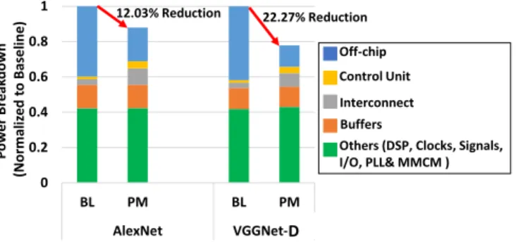
Fig. 12 shows the normalized power consumption of BL and PM for AlexNet and VGGNet-D. We present the results for these two networks here as they represent the highest (AlexNet) and the lowest (VGGNet-D) throughput improvement, and the trend of other networks falls some-where between them. The main overhead of PM is a control unit and an interconnect between the PE cells and memory
banks. The control unit in PM accounts for 4.0% and 3.6% of the total power for AlexNet and VGGNet-D, respectively. The interconnect in PM accounts for 9.3% and 7.6% of the total power for AlexNet and VGGNet-D, respectively. These overheads are higher than those in BL, but the benefits are the flexibility of logical accelerators and the substantial reduction in off-chip traffic. This leads to 12.03% reduction in the total power for AlexNet and 22.27% reduction VGGNet-D, when compared with BL.
6.2 Comparison with State-of-the-Art
In this subsection, we compare the proposed Polymorphic accelerator with three most related state-of-the-art designs. Comparisons are based on the metrics, configurations, and workloads that are reported in the original works. The first compared design is resource partitioning (RP) [33]. Table 2 lists the results of RP and PM for AlexNet on Xilinx Virtex-7 690T FPGA with 32-bit floating-point at 100MHz. Again, the workload and frequency are selected to match with [33]; PM can support different networks, higher frequencies, smaller PE cells, and compact data types.
For an inference operation, the off-chip feature map data transfer is reduced from 52.8MB in RP to only 32.7MB in PM, which is a significant reduction of 38.1%. Throughput is also increased from 113.9 GOPS in RP to 127.7 GOPS in PM, which improves by 12.1%. The main reasons for the improvement are the dynamic adjustment of PE array dimensions and the faster access of feature maps due to FM Push-Pull procedures. On-chip power consumption is slightly higher in PM because PM processes more data per second. However, the reduction in off-chip traffic can likely offset this and result in a lower overall power (due to the lack of information on RP, we could not estimate off-chip power precisely, but the overall power should be lower in PM given the breakdown distribution in Fig. 12). We also evaluate the benefits of PM over RP when several networks need to be processed by a single accelerator. Both RP and PM designs are optimized to process VGGNet-D, SqueezeNet, and AlexNet under the same setup. We have observed an average of 1.63x improvement in throughput for PM compared with RP. The reason for this large improvement is that, when RP is optimized for multiple networks, each partition should be optimized for a greater number of layers compared with the single network case. Thus, it is more likely that a partition may not match well with the dimensions of layers in different networks. In contrast, PM is able to reconfigure for different networks, thereby having a higher overall performance. Note that the BRAM usage 49% is smaller than that in Table1 because RP does not need to use all the memory in Virtex-7 690T. We limit the offline routine of PM to not exceed this number. The resulting PM uses less memory while improving throughput.
Table 3 compares PM with the state-of-the-art single CNN layer dataflow [25]. This dataflow reduces the off-chip data movement and increases the PE array utilization only for CNN layers (e.g., does not work for LSTM or MLP). However, to the best of our knowledge, among the approaches that focus on single CNN layer processing, this work achieves the best results. The single layer dataflow is implemented on Altera Arria-10 GX 1150 FPGA. For a fair comparison, an equivalent Xilinx FPGA chip in terms of on-chip memory and
the number of DSPs is used in this comparison. As shown in Table 3, the single CNN layer dataflow has a throughput of 645.3 GOPS; whereas PM reaches 809.0 GOPS, which equals an improvement of 25.4%. Again, dynamic adjustment and faster access to data play the main roles here for achieving the improvement.
We have also evaluated the proposed polymorphic ac-celerator against MAERI [22], an acac-celerator with flexible dataflow mapping capability. MAERI is aimed for imple-mentation on ASIC. Therefore, we have projected the poly-morphic design to an ASIC implementation for comparison. The area and power of different hardware resources such as multiplier, adders, and memory banks are obtained from Synopsys Design Compiler, and then imported to the routine explained in section 5 for projection at same technology node
(28nm). Under the same area constraint (6mm2) and other
settings, we have observed an 1.52x throughput improve-ment for AlexNet at 200MHz compared with the results from the MAERI paper. This improvement mainly comes from the fact that PM achieves reconfigurability through logicial accelerators and polymorphism, thus has a much smaller area for interconnects. In contrast, MAERI requires a complex interconnect between adders, multipliers, and local buffers. 6.3 Scalability
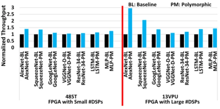
In this subsection, we investigate the scalability of the polymorphic approach when more resources are provided. Here, resources refer to the computing resources (i.e., DSP slices) and on-chip memory resources (i.e., BRAMs and URAMs). Two extreme cases are considered: an FPGA with a small resource budget (Xilinx Virtex-7 485T [9]) and an FPGA with a large resource budget (Xilinx Virtex UltraScale+ VU13P [10]). Due to the lack of access to advanced FPGAs, the throughput is projected for BL and PM following the models and methodology in Section 5.
Fig. 13 compares the normalized throughput for both designs in 32-bit floating-point. The results for the small and large FPGAs are separated by the red line. It can be seen that scaling resources leads to higher throughput improvement of PM over BL for every network, with the largest change observed on AlexNet (1.4x throughput improvement on 485T to 2.95x on VU13P). This excellent scalability of PM is attributed to two factors. First, on the PM side, more PE cells give better flexibility and more choices for PM to match PE array dimensions with layer dimensions. Second, on the BL side, when a large number of PE cells is available, it is more prone to have a mismatch between PE array dimensions and layer dimensions, thereby resulting in more idle PE cells. 6.4 Compact Data Type
Using compact data types is a major trend to improve the efficiency of DNN accelerators [27]. To investigate the effectiveness of the proposed PM approach for compact data types, we examine the PM design for 16-bit fixed-point representation on VU13P FPGA, with same methodology used in previous subsections. The throughput is improved by 9.6x for AlexNet, 4.53x for SqueezeNet, 1.53x for VGGNet-D, 2.21x for GoogLeNet, 1.92x ResNet-34, 1.82x for LSTM and 2.29x for MLP. These results are expected because by using compact data types, more computing units are available for