Wireless Test Bench Simulation
ii
Agilent Technologies makes no warranty of any kind with regard to this material, including, but not limited to, the implied warranties of merchantability and fitness for a particular purpose. Agilent Technologies shall not be liable for errors contained herein or for incidental or consequential damages in connection with the furnishing, performance, or use of this material.
Warranty
A copy of the specific warranty terms that apply to this software product is available upon request from your Agilent Technologies representative.
Restricted Rights Legend
Use, duplication or disclosure by the U. S. Government is subject to restrictions as set forth in subparagraph (c) (1) (ii) of the Rights in Technical Data and Computer
Software clause at DFARS 252.227-7013 for DoD agencies, and subparagraphs (c) (1) and (c) (2) of the Commercial Computer Software Restricted Rights clause at FAR 52.227-19 for other agencies.
© Agilent Technologies, Inc. 1983-2007.
395 Page Mill Road, Palo Alto, CA 94304 U.S.A.
Acknowledgments
Mentor Graphics is a trademark of Mentor Graphics Corporation in the U.S. and other countries.
Microsoft®, Windows®, MS Windows®, Windows NT®, and MS-DOS® are U.S. registered trademarks of Microsoft Corporation.
Pentium® is a U.S. registered trademark of Intel Corporation.
PostScript® and Acrobat® are trademarks of Adobe Systems Incorporated. UNIX® is a registered trademark of the Open Group.
Java™ is a U.S. trademark of Sun Microsystems, Inc.
SystemC® is a registered trademark of Open SystemC Initiative, Inc. in the United States and other countries and is used with permission.
iii
Contents
1 Wireless Test Bench Basics
Introduction... 1-1 Wireless Test Benches, Sources, and Expressions ... 1-1 Required Licenses... 1-2 Wireless Test Bench Models ... 1-3 Wireless Sources ... 1-5 Wireless Expressions ... 1-5 Wireless Examples ... 1-6
2 Using Wireless Sources and Expressions
Introduction... 2-1 Setting up a Circuit Envelope Analysis... 2-1
3 Using Wireless Test Bench Models
Introduction... 3-1 Importing Wireless Test Bench Models ... 3-1 Wireless Test Bench Models Update... 3-4 Preparing an RFIC Design for WTB Analysis... 3-4 Setting Up a Wireless Test Bench Analysis... 3-5 Opening a Wireless Test Bench Model... 3-6 Setting up a Wireless Test Bench Model ... 3-7 Connecting to an RF Device Under Test ... 3-8 Setting Required Parameters ... 3-9 Setting Circuit Envelope Analysis Parameters ... 3-10 Setting the Fundamental Tones... 3-11 Setting Optional Model Parameters... 3-13 Getting Help on WTB Models ... 3-13 Setting Optional Analysis Parameters ... 3-14 Setting Automatic Verification Modeling Parameters ... 3-14 Automatic Verification Modeling Parameters... 3-18 Running a Simulation ... 3-20 Performing Sweeps, Monte Carlo/Yield Analysis, and Optimizations... 3-21
4 Using Instrument Connectivity
Introduction... 4-1 Connecting to Instruments... 4-1 Instrument Discovery... 4-1 Compatibility with Agilent Technologies Instruments ... 4-3
5 Viewing Simulation Results
iv
6 Wireless Measurement Definitions
Introduction... 6-1 Transmission Test Measurements ... 6-1 RF Envelope... 6-1 Constellation... 6-1 Power ... 6-5 Spectrum ... 6-8 EVM... 6-10 Receiver Test Measurements ... 6-12 BER Measurements ... 6-12 Eb/No Definition ... 6-12 References ... 6-16
A Creating Wireless Test Bench Designs for RFDE
Introduction... A-1 Creating a Wireless Test Bench Design ... A-1 Wireless Test Bench Design Examples ... A-2 Setting the Units for WTB Design Parameters ... A-2 Categorizing WTB Design Parameters ... A-3 Information Parameters ... A-3 Verifying a WTB Design in ADS ... A-3 Exporting a WTB Design to RFDE ... A-4 WTB Design User Interface Attributes... A-4 Creating a Results Display for WTB Designs ... A-5 Circuit Envelope Parameters... A-6
Introduction 1-1
Chapter 1: Wireless Test Bench Basics
Introduction
RFDE wireless test benches enable system designers to make wireless system
measurements available to RFIC designers to validate their RFIC designs intended for use with wireless systems.
Previously, RFIC designers using RF Design Environment used traditional Analog/RF measurements such as spectrum, TOI, etc. to validate their designs. Empirical methods used to map Analog/RF measurements to determine wireless system performance were error prone. Typically, they could not perform more
complex wireless system measurements successfully such as EVM and BER. And, a system designer using Advanced Design System’s Ptolemy simulator could not easily deliver a system test bench to the RFIC designer for more accurate and complete RFIC verification.
A similar capability for strictly RFIC designs is available in RFDE called wireless test bench; refer to ADS Ptolemy in AMSD-ADE documentation for details.
Wireless Test Benches, Sources, and Expressions
The pre-configured wireless test bench models delivered with RFDE enable the RFIC designer to validate their designs in wireless systems. The WTB models are complete, so the RFIC designer does not need to know the internal test bench details.System designers can also make custom wireless system measurements available to RFIC designers to validate their designs in RFDE. For details, refer to Appendix A, Creating Wireless Test Bench Designs for RFDE.
The WTB analysis available in the RFDE ADSsim simulator’s list of analyses provides easy access to the WTB models. Simply select a model within the WTB analysis. The RFIC designer need only connect their RFIC design (the RF design under test), specify test bench test frequency and/or power levels, and rely on the other default settings.
RFDE WTB models are provided for transmitter and receiver RFIC testing.
Transmitter models provide standards-specific wireless transmitter tests such as constellation, CCDF, and EVM; transmitter models can be linked to Agilent signal generator test instruments to further enable designers to use the same test signals
1-2 Wireless Test Benches, Sources, and Expressions
from the WTB models to test their RFDE RFIC designs as well as hardware
prototype of their RFIC designs. Receiver models provide standards-specific wireless receiver tests such as BER.
The RFIC designer typically should use the WTB analysis after doing traditional measurements to achieve an acceptable performance from the RFIC. In the initial design stages the RFIC designer may have to stimulate the design with proper wireless standard signals.
Wireless sources are provided with RFDE as part of the adsLib library. Their use model is similar to other adsLib power sources such as P_1Tone. These configurable source components can be placed directly in the RFIC schematic.
Wireless sources generate RF signals that can be used in traditional simulations. Additionally, these can be used for wireless system measurements, such as WLAN EVM, using the set of wireless expressions. These wireless expressions are available in the Expression Builder under the Env analysis type. For more complex receiver measurements, such as BER, you must use the wireless test bench models using the WTB analysis.
The wireless sources and expressions are useful in the initial phases of the RFIC development for traditional Analog/RF measurements. As the design matures, the RFIC designer must use WTB analysis and the corresponding wireless test bench models for more complete transmitter and transmitter system verification.
Required Licenses
Licenses required to use wireless test bench models, wireless sources, and wireless expressions are listed in Table 1-1.
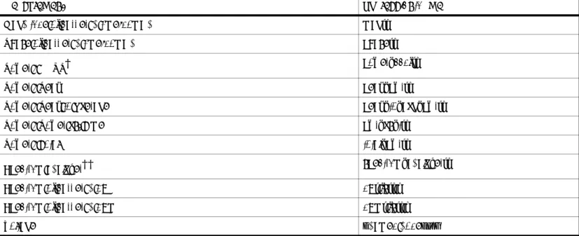
Table 1-1. Required Licenses
Feature Required Licenses
Wireless Test Bench Models, Sources, and Expressions rfde_environment rfde_circuit_int Wireless Test Bench Models also require: rfde_wtb_int
sim_systime 3GPP FDD W-CDMA Wireless Design Library
for 3GPP FDD Wireless Test Bench Models, Sources, and Expressions
mdl_wcdma3g
TD-SCDMA Wireless Design Library
for TD-SCDMA Wireless Test Bench Models, Sources, and Expressions
mdl_tdscdma
Note: Custom WTB models created in Advanced Design System may include models that require additional licenses to use the custom WTB models in RFDE.
Wireless Test Benches, Sources, and Expressions 1-3
Wireless Test Bench Models
Table 1-2 lists pre-configured wireless test bench models installed with RFDE. These test benches provide comprehensive transmitter and receiver testing for 3GPP FDD, TD-SCDMA, and WLAN technologies. All measurements are performed according to wireless technology industry standard specifications. For details about using these models, see the online documentation:
3GPP FDD Wireless Test Benches TD-SCDMA Wireless Test Benches WLAN Wireless Test Benches
Note Custom test benches can be created in ADS. For details, refer to Appendix A, Creating Wireless Test Bench Designs for RFDE.
WLAN Wireless Design Library
for WLAN Wireless Test Bench Models, Sources, and Expressions
mdl_wlan
Connection Manager (for WTB models with instrument connectivity) download to Agilent ESG instruments
link_connect_mgr
Connections to Agilent network analyzers link_measampmodeling
Table 1-2. RFDE Wireless Test Bench Models
WTB Model Measurements ESG Link
3GPPFDD_BS_TX:
3GPP FDD Base Station Transmitter Test
RF Envelope, Power, ACLR, Occupied Bandwidth, CDP, PCDE, EVM
Signals can be sent to an ESG
3GPPFDD_UE_TX:
3GPP FDD User Equipment Transmitter Test
RF Envelope, Power, ACLR, ACLR ST, Occupied
Bandwidth, CDP, PCDE, EVM
Signals can be sent to an ESG
3GPPFDD_BS_RX:
3GPP FDD Base Station Receiver Test
Ref Level, Dynamic Range, ACS, Blocking, Intermod 3GPPFDD_UE_RX:
3GPP FDD User Equipment Receiver Test
Ref Level, Max Level, ACS, Blocking, Intermod
WLAN_802_11a_TX:
WLAN 802.11a/11g Transmitter Test
RF Envelope, Power,
Constellation, Spectrum Mask, EVM
Signals can be sent to an ESG
Table 1-1. Required Licenses (continued)
Feature Required Licenses
Note: Custom WTB models created in Advanced Design System may include models that require additional licenses to use the custom WTB models in RFDE.
1-4 Wireless Test Benches, Sources, and Expressions
WLAN_802_11a_RX_ACR: WLAN 802.11a/11g Receiver Test
Receiver Adjacent Channel Rejection Test
WLAN_802_11a_RX_Sensitivity: WLAN 802.11a/11g Receiver Test
Minimum Input Power Sensitivity
WLAN_802_11b_TX:
WLAN 802.11b/11g Transmitter Test
RF Envelope, Power,
Constellation, Spectrum Mask, EVM
Signals can be sent to an ESG
WLAN_802_11b_RX_Sensitivity: WLAN 802.11b/11g Receiver Test
Minimum Input Power Sensitivity
TDSCDMA_DnLnk_TX:
TD-SCDMA Downlink Transmitter Test
RF Envelope, Constellation, Power, Spectrum, EVM
Signals can be sent to an ESG
TDSCDMA_UpLnk_TX:
TD-SCDMA Uplink Transmitter Test
RF Envelope, Constellation, Power, Spectrum, EVM
Signals can be sent to an ESG
TDSCDMA_DnLnk_MultiCarrier_TX:
TD-SCDMA Downlink Transmitter Test for Multi-carrier Signals
Power, Spectrum
TDSCDMA_DnLnk_RX_ACS: TD-SCDMA Downlink Receiver Test
Downlink Adjacent Channel Selectivity Test
TDSCDMA_UpLnk_RX_Sensitivity: TD-SCDMA Uplink Receiver Test
Uplink Minimum Input Level Sensitivity Test
Table 1-2. RFDE Wireless Test Bench Models (continued)
Wireless Test Benches, Sources, and Expressions 1-5
Wireless Sources
Table 1-3 lists the RFDE wireless sources. These wireless sources provide standard compliant RF signals for WLAN, TD-SCDMA, and 3GPP FDD wireless technologies. In addition to the RF signal, the TD-SCDMA and 3GPP FDD sources provide
baseband I and Q signals. These sources are highly configurable and can generate signals with different rates, power levels, impairments, etc. For details about these sources, see the online Components documentation Sources-DSP-Based.
Wireless Expressions
Table 1-4 lists the RFDE wireless expressions. These expressions are used to perform measurements commonly used for testing 3GPP FDD, WLAN, and TD-SCDMA
transmitters.
These expressions are available in the Expression Builder under Env Analysis Type. The Expression Builder also provides versions of these expressions that can be used with differential voltage signals. See Expression Builder in the Measurement
Expressions documentation for details. See the Measurement Expressions
documentation for details about using these expressions. Table 1-3. RFDE Wireless Sources
Source Name Description
WLAN_802_11a WLAN 802.11a (OFDM) source WLAN_802_11b WLAN 802.11b (CCK/PBCC) source TDSCDMA_DnLink TD-SCDMA downlink source TDSCDMA_UpLink TD-SCDMA uplink source 3GPPFDD_DnLink 3GPP FDD downlink source 3GPPFDD_UpLink 3GPP FDD uplink source
Table 1-4. RFDE Wireless Expressions
Measurement Expression Name
Baseband signal in time-domain real()
EVM measurement for WLAN DSSS/CCK/PBCC evm_wlan_dsss_cck_pbcc() EVM measurement for WLAN OFDM evm_wlan_ofdm()
† The power_ccdf_ref() expression, which generates a reference curve for the Power-CCDF measurement, can be used in transmitter
testing. This expression is not available in the Expression Builder.
†† The spectrum_analyzer() and fs() expressions can be used for spectrum measurement. Although spectrum_analyzer() uses fs()
1-6 Wireless Test Benches, Sources, and Expressions
Wireless Examples
RFDE examples demonstrate how to use wireless test benches, sources, and
expressions. To access these examples, from the CIW window, choose Tools > RFDE
Examples > Open Examples; select WLAN, TDSCDMA, or WCDMA3G; then select an
example from the Top-level cells list. Examples use the following naming convention: • Wireless test bench models: <standard_name>_WTB_Test.
• Wireless sources and expressions: <standard_name>_Source_Expression_Test.
Magnitude of carrier in time-domain mag() Phase of carrier in time-domain phase()
Power - CCDF† power_ccdf()
Power - Peak peak_pwr()
Power - Peak to Average peak_to_avg_pwr()
Power - Power vs. Time pwr_vs_t()
Power - Total total_pwr()
Spectrum analyzer†† spectrum_analyzer()
Spectrum of carrier in dB dB( fs() )
Spectrum of carrier in dBm dBm( fs() )
Voltage <named node>[1]
Table 1-4. RFDE Wireless Expressions
Measurement Expression Name
† The power_ccdf_ref() expression, which generates a reference curve for the Power-CCDF measurement, can be used in transmitter
testing. This expression is not available in the Expression Builder.
†† The spectrum_analyzer() and fs() expressions can be used for spectrum measurement. Although spectrum_analyzer() uses fs()
Introduction 2-1
Chapter 2: Using Wireless Sources and
Expressions
Introduction
The Wireless Sources available in RF Design Environment are useful for traditional Analog/RF measurements. In the initial stages of an RFIC design you may need to stimulate the design with proper wireless standard signals. Wireless sources
generate complex signals useful for traditional measurements. Additionally, these can be used for wireless system measurements, such as WLAN EVM, using the set of Wireless Expressions.
The Wireless Sources are provided as part of the adsLib library in RFDE for wireless standard signal generation. These are configurable source components and their use model is similar to adsLib power sources such as P_1Tone. Wireless sources can be used in different analyses such as Circuit Envelope, and S-parameter just like other adsLib library sources.
The Wireless Expressions can be found in the Expression Builder under Env analysis type. For more complex measurements, such as BER, you must use the Wireless Test Bench Models using the WTB analysis. For details about using the Wireless Test Bench Models, refer to Chapter 3, Using Wireless Test Bench Models.
Setting up a Circuit Envelope Analysis
In the early stages of RFIC design you can use the wireless sources to generate the standard wireless signal required to stimulate the RFIC design under test (DUT). These sources, part of the adsLib library under Sources Modulated, can be placed on the schematic design similar to other adsLib source components. The sources are typically used with Circuit Envelope analysis.
To set up the DUT for a Circuit Envelope analysis:
1. Open the Analog Design Environment window. This can be done from the schematic window using Tools > Analog Design Environment.
2. In the Analog Design Environment window, select Analyses > Choose to open the Choosing Analyses window.
2-2 Setting up a Circuit Envelope Analysis
3. Choose the Env analysis. Update the parameters with the stop time, time step, and frequencies of interest.
To set up wireless expressions for measurements:
1. In the Analog Design Environment window, select Outputs > Measurement Expressions.
2. In the Measurement Expressions window, choose Build Expressions.
3. In the RFDE Expression Builder window, select the Env analysis type. The list of Measurements includes wireless expressions in the list of Env expressions. 4. Select the expression, the DUT node to operate on, and set the parameters.
Click OK. The expression appears in the string field in the Measurement Expressions window.
5. In the Measurement Expressions window, on the left side of the string field, add the expression name or the equation’s left side followed by = . Click Add to add this expression to the expression list.
Introduction 3-1
Chapter 3: Using Wireless Test Bench
Models
Introduction
Wireless test bench simulation is used to perform complex wireless system
measurements using wireless test bench models. Pre-configured models are installed with RFDE; custom models created by system designers using ADS can be selected to perform other measurements (for information, refer to Appendix A, Creating
Wireless Test Bench Designs for RFDE).
WTB simulation uses Circuit Envelope analysis along with the ADS Ptolemy Data Flow (DF) controller to perform Analog/RF and system cosimulation. Each wireless test bench model is packaged such that the RFIC designer avoids working with DF analysis parameters. The RFIC designer can change and control the underlying Circuit Envelope analysis parameters on the Wireless Test Bench Options window.
Importing Wireless Test Bench Models
System designers can create wireless test bench models in ADS and export them to RFDE. RFIC designers can import these WTB models into RFDE to perform complex wireless system measurements. In the Wireless Test Bench Path Editor window, you can specify directory paths to ADS projects that contain WTB models created and exported by system designers. These paths are used to import WTB models so they are available when you need to use a model.
3-2 Importing Wireless Test Bench Models
For details about creating and exporting WTB models, refer to Appendix A, Creating Wireless Test Bench Designs for RFDE.
To specify the paths to wireless test bench models:
1. In the Analog Design Environment window, select Tools > WTB Path Editor to open the Wireless Test Bench Path Editor window.
2. Click Browse to open the File Browser window. Locate the path to the project containing exported WTB model(s). Click OK or Apply. The selected path appears in the Path Editor’s field Select ADS Project to Import WTB from. 3. Click Add to move the path selection into the list area.
To change the specification of a path in the list:
1. Select a path in the list area that you want to change.
2. The path appears in the field Select ADS Project to Import WTB from. Type in any changes.
or
Click Browse to open the File Browser window. Locate the path to the project containing exported WTB model(s). Click OK or Apply. The selected path appears in the Path Editor’s field Select ADS Project to Import WTB from. 3. Click Change to replace the path selected in the list area.
Importing Wireless Test Bench Models 3-3 • Select a path in the list area, then
Click Delete to remove the path from the list.
3-4 Preparing an RFIC Design for WTB Analysis
Wireless Test Bench Models Update
When you are ready to use a WTB model in a WTB analysis, the WTB models are imported or updated when you click Edit in the Choosing Analyses window. The WTB models are read and imported from the list of paths specified in the Wireless Test
Bench Path Editor. The list is read from top to bottom.
Each time you click OK or Apply in the Wireless Test Bench Path Editor, all of the models are checked to see if they are new or have been updated. An exported WTB model file is imported only if it is newer than the model file imported previously. The pre-configured WTB models installed with RFDE are always imported last after all of the models in the user-specified paths. So a WTB model in an ADS project path specification that is earlier in the list can override the WTB model with same name specified later in the list. You can use this feature to override the pre-configured WTB models. For a summary of the pre-configured WTB models, see “Wireless Test Bench Models” on page 1-3.
Preparing an RFIC Design for WTB Analysis
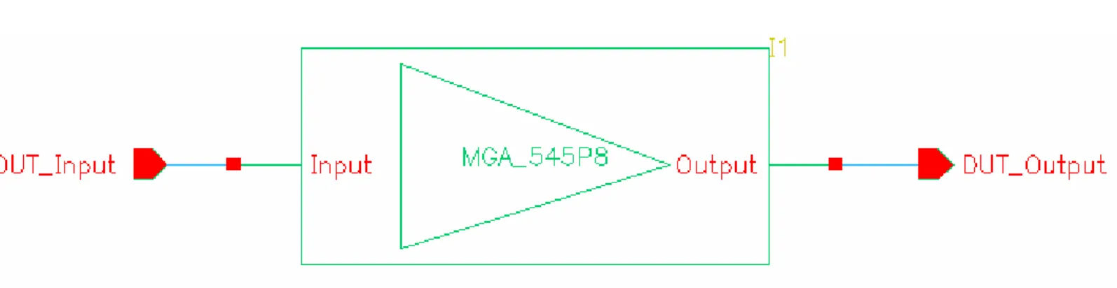
The DUT must contain an input and an output Pin connected to the node or wire to which the WTB model must be connected. With the design open in the schematic window, add pins to the design using Add > Pins. It is not necessary to add other input and output components because the WTB model provides the input source signal to simulate the DUT and appropriate termination to perform various measurements. Figure 3-1 shows an example design with pins added.
Note During a WTB analysis, naming a wire on the DUT will not produce data for that named node in the final dataset.
Setting Up a Wireless Test Bench Analysis 3-5
Setting Up a Wireless Test Bench Analysis
Before setting up a WTB analysis you must have a valid design selected in the Analog Design Environment window and the simulator must be set to ADSsim (Setup >
Simulator/Directory/Host). Then choose the wtb analysis (Analyses > Choose).
After choosing the wtb analysis, open a wireless test bench model, connect the RFIC design ports to the WTB model, set the required parameters, and set optional
parameters if necessary. These topics are discussed in the following sections: • “Opening a Wireless Test Bench Model” on page 3-6
• “Connecting to an RF Device Under Test” on page 3-8 • “Setting Required Parameters” on page 3-9
• “Setting Optional Model Parameters” on page 3-13 • “Setting Optional Analysis Parameters” on page 3-14
3-6 Opening a Wireless Test Bench Model
Opening a Wireless Test Bench Model
Before opening any wireless test bench model, they must be available in any of the following locations:
• Under $HPEESOF_DIR/adsptolemy/wtb where RF Design Environment is installed.
• In the user-specified WTB model path.
• In the ADS project containing the exported WTB models and specified in the Wireless Test Bench Path Editor.
To open a wireless test bench model:
1. In the Choosing Analyses window, click Edit in the Wireless Test Bench Setup
area. The Wireless Test Bench Setup window opens where you can select a wireless test bench model. Clicking Edit also updates WTB models imported into RFDE. See “Wireless Test Bench Models Update” on page 3-4 for details.
Note The Wireless Test Bench Setup window will not open if WTB models are not found.
Setting up a Wireless Test Bench Model 3-7 2. In the Wireless Test Bench Setup window, select the wireless standard from the
Category drop-down list.
The pre-configured models installed with RFDE are organized into TD-SCDMA, WCDMA3G, and WLAN categories. If a system designer exports any WTB model from ADS, a new category is added based on the name of the ADS project from which the WTB design was exported.
3. Select the test bench model from the Test Bench drop-down list, which is a list of WTB models available for a selected category.
Each time a WTB model is selected the ports and parameters lists are automatically updated in the Wireless Test Bench Setup window.
You are now ready to connect the WTB model’s input and output to the RFIC DUT pins, select measurements, and set parameters. See “Setting Circuit Envelope
Analysis Parameters” on page 3-10, and “Setting up a Wireless Test Bench Model” on page 3-7.
Setting up a Wireless Test Bench Model
Use the Wireless Test Bench Setup window to set up a WTB for system verification measurements on the RFIC design.
You must connect the RFIC DUT’s ports to the WTB model, set the required parameters, and set optional parameters as necessary. The required parameters include setting simulation frequencies and selecting measurements; at least one measurement must be enabled for successful simulation. Optional parameters
provide additional control of the selected measurements. These topics are discussed in the following sections:
• “Connecting to an RF Device Under Test” on page 3-8 • “Setting Required Parameters” on page 3-9
• “Setting Optional Model Parameters” on page 3-13
The following table lists the various parameter data entry fields found in the Wireless
3-8 Connecting to an RF Device Under Test
Connecting to an RF Device Under Test
You must identify the port connections between the RFIC DUT and the WTB model in the Wireless Test Bench Setup window. Simply connect the WTB RF_out and
Meas_in ports to the DUT by identifying the appropriate pin names.
Parameter Field Type Description
String data entry field Used to enter integer, real, complex, or string type of scalar data. Array and string type data must be enclosed in quotes.
String data entry field with multiple choices
This gives you multiple choices for the value of the parameter to select from. The pull down list field also enables you to type in the data directly. The last choice in the list specifies what the type-in value can be, such as an option index, a real value, etc. Use this mode to assign a variable to this type of parameter; then use the variable to either sweep or optimize the parameter. Information fields This non-editable information field provides information on a certain aspect of the WTB model. Instrument selection field This is a string data entry field followed by a button to launch the instrument-selection user
interface. This type of parameter is used only when you enable ESG download. You can enter the instrument address directly or use the button to launch the instrument-selection user interface to interactively select the instrument and update the address.
Setting Required Parameters 3-9 To connect the ports:
1. Open the RFIC design (the DUT) in a schematic window. The design in the schematic must match the design indicated in the Analog Design Environment window from where the Choosing Analyses and the Wireless Test Bench Setup windows were opened.
2. Add input and output pins to the RFIC design using Add > Pin in the schematic window.
3. In the Wireless Test Bench Setup window Pin Connections area, click Select Pin
next to the field linked to RF_out, then click the input pin in the schematic. The input pin name appears in the field between the ports, indicating that the
RF_out port is connected to the DUT input.
4. Click Select Pin next to the field linked to Meas_in, then click the output pin in the schematic. The output pin name appears in the field between the ports, indicating that the Meas_in port is connected to the DUT output.
You should now set the required parameters; see “Setting Required Parameters” on page 3-9.
Setting Required Parameters
After connecting the WTB model and DUT ports, set the model parameters in the Required Parameters area of the Wireless Test Bench Setup window. The number of parameters will vary between different models. These parameters control the
simulation and identify the selected measurements. They must have valid values and cannot be left blank. For detailed information about setting these parameters, click
WTB Model Help.
Important You must set the required frequencies and select at least one measurement for successful simulations.
Note To reset all parameter values to their default or standard factory-set values, click Reset To Standard located at the top of the Wireless Test Bench Setup window.
3-10 Setting Required Parameters
Setting Circuit Envelope Analysis Parameters
The WTB analysis is a cosimulation between an Env (Circuit Envelope) analysis and a DataFlow analysis to verify an RFIC design’s system performance. The DataFlow analysis is pre-configured with the WTB model. When you select the WTB analysis in the Choosing Analyses window, the contents are similar to Env analysis. The Wireless
Test Bench Options window is the same as Circuit Envelope Options except the
Wireless Test Bench Options window contains Automatic Verification Modeling (AVM)
parameters for faster cosimulation.
The RFIC designer must configure the Circuit Envelope analysis to ensure proper simulation.
• CE_TimeStep (Circuit Envelope Time Step): set the value based on the information field below this parameter.
• FSource (Source Frequency): This DUT input signal frequency should be added to the Fundamental Tones area in the Choosing Analyses window, based on the frequency conversion characteristics of the DUT’s input side.
• FMeasurement (Measurement Frequency): This DUT output signal frequency is used for selected measurements and should be added to the Fundamental Tones
Setting Required Parameters 3-11 area in the Choosing Analyses window, based on the frequency conversion characteristics of the DUT’s output side.
Setting the Fundamental Tones
Use the Fundamental Tones table to enter the frequencies for the underlying Circuit Envelope simulation. This table must contain all of the different frequencies such as
FSource and FMeasurement that are set in the Wireless Test Bench Setup window.
The WTB model uses these parameters for accurate simulation and measurement. When you click OK or Apply in the Wireless Test Bench Setup, the following actions help complete the frequency information in the Fundamental Tones table:
3-12 Setting Required Parameters
• If the Fundamental Tones table is empty, then a warning appears asking if the frequencies FSource and FMeasurement should be added to the table. Click Yes or No.
• If the Fundamental Tones table contains data and you modify FSource or
FMeasurement, a warning appears stating which of the frequencies have been
modified and that you should make the necessary changes in the Fundamental Tones table.
• If the Fundamental Tones table contains data and you have not modified
FSource or FMeasurement, no message appears even if the frequencies are
inconsistent.
Once the frequency information is correctly added to the table, do not delete these frequencies from the table. You can modify other parameters for a frequency added to the table.
For details about modifying the Fundamental Tones table, see this parameter’s description in the section RFDE Envelope Analysis Parameters in the Circuit
Envelope Simulation documentation.
Simulation stop time is controlled by the selected measurements and their parameter values. The measurements and their parameters are located on the tabs below the Required Parameters area. If necessary for your measurement requirements, set the optional parameters for the WTB model, and for the WTB analysis. See “Setting Optional Model Parameters” on page 3-13, and “Setting Optional Analysis
Setting Optional Model Parameters 3-13
Setting Optional Model Parameters
The WTB model’s optional parameters are located on tabs located in the lower area of the Wireless Test Bench Setup window. Scroll down to see all of the parameters. The parameters on some of these tabs control the simulation run time. You will use these tabs mostly to modify the simulation run time; otherwise, you will rarely need to modify them.
Note To reset all parameter values to their default or standard factory-set values, click Reset To Standard at the top of the Wireless Test Bench Setup window.
Other tabs in this area contain parameters for measurements listed in Required
Parameters. Some of those parameters will also control the simulation run time. You
may need to change parameters for the measurements you have selected.
For detailed information about setting these parameters, click WTB Model Help.
Use the left and right arrows beside the tabs to scroll through them. Click a tab label to view its parameters.
Getting Help on WTB Models
Detailed documentation is available from the Wireless Test Bench Setup window: • For documentation about the currently selected, pre-configured model, click
WTB Model Help.
• For documentation about using the Wireless Test Bench Setup window, click
3-14 Setting Optional Analysis Parameters
Setting Optional Analysis Parameters
To set the optional WTB analysis parameters, click Options on the Choosing Analyses window when WTB analysis is selected. This opens the Wireless Test Bench Options window. The parameters set the underlying Circuit Envelope optional parameters. For faster cosimulation, enable the Automatic Verification Modeling (AVM).
For information about using AVM, see “Setting Automatic Verification Modeling Parameters” on page 3-14. For details about the AVM parameters, see “Automatic Verification Modeling Parameters” on page 3-18. For details about the additional, optional Circuit Envelope parameters, see the section RFDE Envelope Analysis
Parameters in the Circuit Envelope Simulation documentation.
Setting Automatic Verification Modeling Parameters
When the Wireless Test Bench Options window is open, enable Automatic Verification
Modeling (AVM) to view and set its parameters.
AVM (also known as Fast Cosim) is a user-selected mode of operation, available for WTB analysis that can significantly speed up Circuit Envelope simulations of
Analog/RF circuits. When this mode is enabled, the analog subcircuit is characterized using a variety of Harmonic Balance simulations at the start of each wireless test bench simulation. During the actual wireless test bench simulation, this
characterization data is then used to predict the response of the subcircuit instead of performing the full circuit simulation at each time point.
Since this characterization is normally done at the start of each WTB analysis sweep based on the full circuit level schematic, the overall capability is basically the same as if the actual circuit level representation is used throughout the Circuit Envelope simulation. For example, optimization of circuit level parameters, or swept
parameters including bias, temperature or swept carrier frequency, will continue to operate as expected. These capabilities do not exist when the circuit is manually replaced with behavioral models.
This ability to predict the modulated response based on the Harmonic Balance
characterization relies on the fact that many circuits, when used in relatively narrow band modulated applications, can have their nonlinearity represented as a static nonlinearity that is strictly a function of the instantaneous amplitude of the carrier. Many of these circuits (amplifiers and mixers) have little or no frequency response over the modulation bandwidth of interest; any frequency response effects that do
Setting Optional Analysis Parameters 3-15 exist can often be represented as a linear filter on the input or output of the
nonlinearity.
Each output of the Analog/RF subcircuit is then characterized by the equation:
The Pk(mag) functions are determined by the swept amplitude Harmonic Balance simulation. The HarmGain is the harmonic gain determined from the harmonic indices of the input and output frequencies.
If phase characterization has been enabled (setting the Num. of phase pts parameter to a non-zero value) each output is then characterized by this modified equation:
In this case, Pk(mag, phase) functions are determined by a 2D swept amplitude and swept phase Harmonic Balance simulation.
If the subcircuit nonlinearities are a function of the input phase, as in a nonlinear IQ demodulator, then the amplitude-only characterization is not accurate and the
2-dimensional amplitude and phase characterization must be used.
Note that the magnitude-only characterization assumes the output phase can be determined from the harmonic indices of the input and output frequencies. In certain rare cases, this can be ambiguous. For example, if the input frequency is fund1 and the output frequency is 2*fund1, then the simulator assumes the output signal is generated by doubling the input frequency and so the input phase is doubled. However, if this 2*fund1 output frequency is actually generated by mixing with another LO source at the fund1 frequency and the phase relationship is supposed to be linear, then the AVM (Fast Cosim) results will be incorrect. If the mixer LO is operating at an independent fund2 frequency, with a mixer output at fund1 + fund2, then the HarmGain of 1.0 is correctly determined. So, as with the IQ demodulator, if there are circuit sources operating at the same frequency as the input signal, caution must be used when enabling this AVM (Fast Cosim) mode, and the 2D amplitude and phase characterization may be required.
In addition to the swept amplitude characterization, the AVM characterization also includes a small signal Harmonic Balance frequency sweep. In this case, the input amplitude is set to 0, and the small signal frequency is swept between
+/- 0.5/TimeStep. Note that even though the input amplitude is set to 0, a nonlinear analysis is still being done so any frequency translation effects due to internal mixers will be fully captured. An impulse response representing this frequency response can
Outk = (Pk(InputMag)–Pk( )0 )×ejInputPhase×HarmGain+Pk( )0
3-16 Setting Optional Analysis Parameters
then be generated and placed (at the user's choice) on the input or the output of the nonlinear block. An additional delay can be added to the frequency response, so that the impulse can be made a more accurate representation of the frequency response. The user should set the number of frequency points high enough that any frequency response deviations are sufficiently sampled (a minimum of 4 samples every 360 degrees). The maximum duration of the impulse response will be approximately 0.75/FreqSpacing, where
N is determined so that 2N is just larger than the user-specified number of frequency points.
In addition to the amplitude and frequency response characterization, nonlinear noise characterization is also done. A single value for the equivalent input noise for each output is determined, then added to the input signal prior to the above
nonlinear and frequency response effects. In the case of multiple outputs, these equivalent noise sources are uncorrelated. So any correlation of the Analog/RF
subcircuit added noise between multiple outputs is lost during this AVM (Fast Cosim) mode. This noise characterization is implemented by selecting Turn On All Noise in the Envelope parameter group in the Options window.
In certain cases, the time spent doing this characterization can be eliminated if the user requests that the simulator use previous characterization. Once this mode is selected, then the user must make sure that the previous characterization is still valid, and that circuit parameters have not been changed (perhaps by optimization), biases have not changed, carrier frequencies have not changed, etc. The circuit should not have changed its connectivity within the WTB analysis environment. Also, the format and data in the dataset must be in the same expected configuration as when it was written by simulator.
In addition to the characterization and implementation portion of the AVM (Fast Cosim) mode, there is also a user-selectable verification step. If the user specifies a non-zero verification Stop Time, then the normal Circuit Envelope simulation is performed in parallel with the fast cosimulation predictions. The error over this verification is then calculated and output to determine how well these predictions are performing. If the behavior is unacceptable, as determined by the Accept Tolerance, then the AVM (Fast Cosim) will be disabled and only the normal Circuit Envelope results will be used. Clearly, if used, this verification time should be set long enough to include a representative portion of the input signal. This may need to take into
FreqSpacing 1
2N× TimeStep ---=
Setting Optional Analysis Parameters 3-17 account the fact that many sources, due to channel filtering, take a while to generate their full amplitude outputs.
Limitations
While you may have selected the AVM (Fast Cosim) mode, it may become disabled if: • The RF DUT has more than one input from the WTB model or the input is not
for an RF signal (non-zero carrier frequency).
• The CE_TimeStep is not an integer submultiple of the WTB_TimeStep. See the specific WTB documentation to understand how the WTB_TimeStep is set. It cannot be set directly by the user and is set by derivation from the other WTB model parameters.
• Verification was enabled but performance did not meet an acceptance level. • The Envelope analysis includes an oscillator analysis.
• The input frequency was a mixing term and not harmonically related to a single fundamental.
• The input frequency does not exactly match an Envelope analysis frequency. • There was a problem reading the previously generated dataset.
Additional limitations of the AVM (Fast Cosim) mode, that may not be automatically detected by the simulator unless verification is enabled, include:
• Envelope analyses parameters such as the Freq parameters should not be swept or optimized.
3-18 Setting Optional Analysis Parameters
Automatic Verification Modeling Parameters
These parameters enable and control the Automatic Verification Modeling (AVM) mode and are only applicable when the Wireless Test Bench Analysis is selected for use with a Ptolemy cosimulation. The following table describes the parameter details. Names listed in the Parameter Name column are used in netlists.
Table 3-1. Wireless Test Bench Analysis AVM Parameters
Setup Dialog Name Parameter Name Description
Automatic Verification Modeling (AVM)
AVM This enables the Automatic Verification Modeling (AVM) mode to be used for the Analog/RF subcircuit. If AVM (Fast Cosim) is not possible for this subcircuit, then a warning will be output and regular Circuit Envelope Cosimulation will be performed.
Max Input Power (dBm) ABM_MaxPower This specifies the maximum input power to this Analog/RF subcircuit that will be used during the AVM (Fast Cosim) characterization phase. Excessively high values will take longer to characterize due to potentially more difficult circuit convergence. If the input power during the cosimulation exceeds this value, a warning will be generated since the AVM (Fast Cosim) results will no longer be accurate.
Number of Amplitude Points ABM_AmpPts This sets the number of linear amplitude points between 0 and the full scale value defined by the Max Input Power. Depending on how much variation there is in the output vs. input amplitude characterization, more amplitude points may be needed to achieve optimum accuracy at a cost of additional characterization time. Due to the continuation nature of the swept amplitude harmonic balance characterization when not using Krylov modes, the cost of additional amplitude points is usually small. In addition to these linear spaced points, the characterization adds an additional power point every 6 dB down to a value 100 dB below the Max Input Power.
Number of Phase Points ABM_PhasePts Any value greater than 0 will enable the characterization to be done as a function of both amplitude and phase. This specifies the number of phase points to be used at each amplitude point. Since this will now be a two dimensional sweep and so will be slower, it should only be used when required, such as with IQ demodulators where the output is a nonlinear function of the input phase. IQ Modems that are linear with phase, but nonlinear with amplitude, do not require phase characterization. Just identify the I/Q pair with the correct polarity in the Node Names section.
Number of Frequency Points ABM_FreqPts This sets the minimum number of small signal frequency points that are used to characterize the Analog/RF subcircuit. The actual number of points is increased to the next highest power of 2 value. These points are spaced between +/- 0.5/TimeStep, where TimeStep is the Step time defined for the Envelope analysis. The maximum impulse duration for this frequency response characterization is determined by this frequency spacing. So the number of frequency points should be greater than the maximum impulse response time of the circuit around the carrier frequency plus any additional Delay specified in the Implementation block, both normalized by the Circuit Envelope TimeStep value.
Setting Optional Analysis Parameters 3-19
Use Previous Characterization
ABM_ReUseData Checking this tell the simulator to re-use any previous characterization that was done for this Analog/RF subcircuit. This characterization is saved in a dataset named after the subcircuit name. This eliminates any overhead time associated with the characterization, but it is then the responsibility of the user to make sure that nothing significant enough has changed (including carrier frequency, time step, bias voltages, temperature, optimization variables, etc.) since the last characterization.
Frequency Compensation ABM_FreqComp This specifies whether or not a frequency compensation filter is to be created for use in the AVM (Fast Cosim) mode. In addition, the user can specify whether this filter is best placed on the input or the output of the nonlinear block. If the modulation is sufficiently narrow that there is not significant frequency response over the envelope bandwidth, then None should be selected. If the frequency response is primarily due to input filtering or transistor bandwidth limitations, then an Input frequency compensation should perform the best. Similarly, if the dominant filtering is at the output of
Analog/RF subcircuit, such as the channel filter, then an Output frequency compensation should be used.
Delay (sec) ABM_Delay This adds additional transit delay to all the outputs of the Analog/RF subcircuit. In cases where this absolute delay is not critical to the overall system
simulation, adding additional delay permits more accurate impulse
implementation of the frequency response. This delay should not exceed half the impulse length, as determined by the frequency response characterization. Verification Time (sec) ABM_VTime If this verification stop time is not zero, then both the normal Envelope
cosimulation and the AVM (Fast Cosim) results are computed. The RMS error between these two results is computed and output after this verification time has ended. This gives an indication as to how well the AVM (Fast Cosim) is matching the Circuit Envelope results.
Verification Acceptance Tolerance
ABM_VTol If the Verification Stop Time has been set, then the resultant RMS error must be less than this value or else the AVM (Fast Cosim) will be turned off and just the normal Envelope cosimulation results will be used for the remainder of the Ptolemy simulation. The stop time must be large enough to account for turn-on delays of filters and to give a sufficiently representative sample of the normal input signal.
Table 3-1. Wireless Test Bench Analysis AVM Parameters
3-20 Running a Simulation
Running a Simulation
After setting the WTB analysis parameters, connecting the WTB model ports to the DUT ports, and setting the model parameters, you can run a simulation. WTB
analysis is supported for remote and distributed simulations. To run a simulation:
1. On the Choosing Analyses window, select Enable, then click OK or Apply.
2. Verify that the Analog Design Environment window indicates Yes for the WTB analysis in the Analyses queue.
During a WTB analysis, do not select any other analysis type. If this happens, the netlisting will error out, suggesting that you turn off other analyses.
Performing Sweeps, Monte Carlo/Yield Analysis, and Optimizations 3-21
Performing Sweeps, Monte Carlo/Yield Analysis, and
Optimizations
WTB model parameters can be included in Parameter Sweep, Monte Carlo/Yield Analysis, and Optimization Analysis. These are available in the Analog Design Environment window on the Tools menu. The simulation start and stop are not
controlled from the Analog Design Environment window; they are controlled from the windows for each of these other tools.
To include WTB model parameters in a sweep, Monte Carlo/yield analysis, and optimization:
1. In the Analog Design Environment window choose Variables > Edit. 2. Define a variable.
This variable must be assigned to the WTB model parameter value. The multiple choice parameters can also be used in a sweep, Monte Carlo/yield analysis, and optimization in a similar manner.
3. Click OK.
For information about Parameter Sweeps, see Parameter Sweeps and Sweep Plans in
RFDE in the chapter Parameter Sweeps and Sweep Plans in the Simulation
documentation.
For information about Monte Carlo/Yield Analysis and Optimizations, see
Introduction 4-1
Chapter 4: Using Instrument Connectivity
Introduction
Transmitter wireless test benches support instrument connectivity. The following sections explain how to connect to instruments and describe the test benches’ compatibility with Agilent Technologies instruments.
Connecting to Instruments
The wireless test benches rely on Connection Manager architecture for instrument connectivity. Connection Manager is the implementation of Agilent Technologies Connected Solutions for RFDE.
A Connection Manager-based simulation is part of the client half of the Connection Manager client/server system, and operates through an instance of the Connection Manager server. You can think of the Connection Manager-based simulation as an interface into the measurement available on the server.
Detailed information about using Connection Manager, including functional concepts and server IO configuration is provided in the Connection Manager documentation. The Connection Manager architecture also provides instrument discovery and measurement exploration.
• Discovery makes it easy to identify the instruments that are connected to your server workstation, enabling the client to easily associate a particular
instrument with a particular measurement.
• Exploration locates measurements on the server and describes a measurement’s capabilities so a client can easily determine what a measurement does and how to use that measurement.
Instrument Discovery
The transmitter test benches provide interactive selection of the instrument before simulation. The Signal to ESG tab includes an Instrument parameter that is set to a string following a specific syntax as shown in this example:
4-2 Connecting to Instruments
To interactively select an instrument:
1. From the Wireless Test Bench Setup window, select the Signal to ESG tab. 2. Look for Instrument in the parameter list.
3. Click the Select Instrument button to access the Set Server dialog box.
4. Enter the DNS hostname or IP address of the workstation on which an instance of the Connection Manager server is running.
5. Enter the port number on which the server is waiting for incoming connection requests. Unless the server settings are changed manually, use the default port number 4790.
6. Click OK to access the Remote Instrument Explorer dialog box.
This dialog box shows the Visa Resource identifiers of all instruments that are currently connected to the workstation running the Connection Manager server. A Visa Resource identifier is like an IP address that can uniquely identify an instrument among all the instruments connected to the workstation through all available interfaces.
Compatibility with Agilent Technologies Instruments 4-3 To map the Visa Resource identifiers to the associated instrument model
number, select one or more of the Visa Resource entries and click the Query Instruments’ IDs button. This tells the Connection Manager server to send the standard IEEE 488.2 identification command *IDN? to the instrument(s). Most modern instruments that understand this command will respond with an
identification string. After all selected instruments are queried, the Instrument IDs are displayed:
7. Select a specific instrument based on the Instrument ID string displayed and click OK.
Click OK on the component dialog box to return to the RFDE dialog box. Click Cancel on any of the dialogs to retain your old settings.
Compatibility with Agilent Technologies Instruments
WLAN test benches, signal sources, and EVM measurements are compatible with the Agilent E4438C ESG Vector Signal Generator, and Agilent 89600 Series VectorSignal Analyzer; details are given in Table 4-1.
TD-SCDMA test benches and signal sources are compatible with Agilent E4438C Signal Generator and Agilent 89600 Series Vector Signal Analyzer; details are given in Table 4-2.
3GPP FDD test benches and signal sources are compatible with Agilent E4406A VSA Series Transmitter Tester, Agilent PSA Series High-Performance Spectrum Analyzer, and Agilent 89600 Series Vector Signal Analyzer; details are given in Table 4-3.
4-4 Compatibility with Agilent Technologies Instruments
For more information about Agilent ESG Series of Digital and Analog RF Signal Generator and Options, visit http://www.agilent.com/find/ESG.
For more information about Agilent PSG Series of Digital and Analog RF Signal Generator and Options, visit http://www.agilent.com/find/PSG.
For more information about Agilent 89600 Series Vector Signal Analyzer and Options, visit http://www.agilent.com/find/89600.
For more information about Agilent PSA series High-Performance Signal Analyzer and Options, visit http://www.agilent.com/find/psa.
Table 4-1. WLAN Agilent Instrument Compatibility Information
WLAN Spec ESG Models VSA Models
SpecVersion= 1999 E4438C, Firmware Revision C.03.40 Option 417 - “802.11 WLAN” Software Personality (Signal Studio)
89600 Series, software version 4.xx/5.xx Option B7R - “WLAN Modulation Analysis”
Table 4-2. TD-SCDMA Agilent Instrument Compatibility Information
TD-SCDMA Spec ESG Models VSA Models
SpecVersion= 6-2002 E4438C, Firmware Revision C.03.40 Option 411 - “TD-SCDMA (TSM)” Software Personality (Signal Studio)
89600 Series, software version 4.xx/5.xx Option B7N - “3G Modulation Analysis”
Table 4-3. 3GPP FDD Agilent Instrument Compatibility Information
3GPP Spec ESG Models VSA Models
SpecVersion= 3-2002 E4438C, Firmware Revision C.03.40
Option 400 - “3GPP W-CDMA FDD” Personality
E4406A, Firmware Revision A.06.03
Option BAF - “W-CDMA” Measurement Personality PSA, Firmware Revision A.04.07
Option BAF - “W-CDMA” Measurement Personality 89600 Series, software version 3.01/4.xx/5.xx Option B7N - “3G Modulation Analysis”
Introduction 5-1
Chapter 5: Viewing Simulation Results
Introduction
Wireless test bench simulation results can be viewed in a data display window. A dataset is generated for each simulation with configurations and data display
template information in which to view results. For automatic plotting, a data display window automatically opens showing the results. For distributed simulation, data display options are provided for viewing plot outputs. The following sections provide information on viewing automatic plotting and distributed simulation results.
For more details regarding using the data display, see the Data Display documentation.
Automatic Plotting
A Data Display/autoplot data display window contains pages that are set up for every measurement enabled in the Wireless Test Bench Setup form.
To enable automatic plotting of results at the end of a simulation:
1. In the Analog Design Environment window, select Results > Data Display Options.
2. In the Data Display Options window, enable the options Open Data Display After Simulation and Enable Automatic Plotting of Outputs.
To perform automatic plotting of a simulation dataset collected earlier:
1. In the Analog Design Environment window, select Results > Data Display Options.
2. In the Data Display Options window, for the option Dataset Used for Automatic Plotting, choose Use most recent dataset, or Prompt for dataset.
3. In the Analog Design Environment window, select Results > Plot Outputs.
If the Analog Design Environment window is opened for a given DUT and the simulation directory is same as the directory used earlier when a successful WTB simulation dataset was generated, then you can see the results without re-running the simulation.
5-2 Distributed Simulation
Distributed Simulation
Wireless test bench models can be used in a distributed simulation with a different model for each simulation, or the same model can be used having different
measurements for each simulation. A dataset is generated for each simulation with configurations and data display template information in which to view results (a data display window does not open automatically).
To plot the most recent generated dataset:
1. In the Analog Design Environment window, select Results > Data Display Options.
2. In the Data Display Options window, for the option Dataset Used for Automatic Plotting, choose Use most recent dataset (the default setting).
3. In the Analog Design Environment window, select Results > Plot Outputs. To select a specific dataset for plotting:
1. In the Analog Design Environment window, select Results > Data Display Options.
2. In the Data Display Options window, for the option Dataset Used for Automatic Plotting, choose Prompt for dataset.
3. In the Analog Design Environment window, select Results > Plot Outputs. The Prompt for Dataset window opens containing the list of datasets generated from a given Analog Design Environment session. The datasets in the list can
include the results of distributed and individual simulations.
4. Select a dataset to use for automatic plotting, and click OK. The selected dataset will contain the data display template names that must be used for automatic plotting. Each different dataset selection will update the final automatic plot window.
Introduction 6-1
Chapter 6: Wireless Measurement
Definitions
Introduction
The following sections briefly describe the most commonly used measurements in transmitter and receiver testing for WLAN, TD-SCDMA, and 3GPP FDD.
• Transmission Test Measurements •“RF Envelope” on page 6-1 •“Constellation” on page 6-1 •“Power” on page 6-5
•“Spectrum” on page 6-8 •“EVM” on page 6-10
• Receiver Test Measurements
•“BER Measurements” on page 6-12 •“Eb/No Definition” on page 6-12
Transmission Test Measurements
RF Envelope
The RF envelope measurement shows the magnitude of the RF signal’s envelope versus time. By observing a signal’s RF envelope versus time you can see the signal’s frame/burst structure. Some wireless standards specify a mask, to which the signal’s RF envelope must conform. The mask is typically specified during the ramp up and ramp down transient of the signal.
Constellation
The constellation measurement shows in a graphical way the general quality of a signal. For a more accurate measurement of a signal’s modulation quality an EVM analysis must be performed.
6-2 Transmission Test Measurements
A constellation measurement is most appropriate when a QAM modulation scheme is used (directly or indirectly; for example WLAN 802.11a uses OFDM modulation, where a set of subcarriers is modulated using some QAM scheme). An ideal QAM signal will have a constellation that consists of a set of distinct points on the IQ plane. Figure 6-1 shows the constellation for an ideal 16-QAM signal. This
constellation has 16 points and is symmetric around the X and Y axes. All points are equally spaced.
Figure 6-1. Constellation for Ideal 16-QAM Signal
Different signal distortions modify the ideal constellation in different ways and so by looking at the constellation you can get some idea of what types of distortions are present in the signal. Figure 6-2 through Figure 6-6 show some examples of how signal distortions appear in the constellation.
Figure 6-2 shows the constellation for a 16-QAM signal with gain imbalance. This can be deduced by the fact that in the ideal constellation the span of the points across both axes is the same (approximately 0.425), whereas in the constellation with the gain imbalance the Y axis has a bigger span (approximately 0.475).
Figure 6-3 shows the constellation for a 16-QAM signal with phase imbalance. This can be deduced by the fact that in the ideal constellation the points are lined up in lines that are parallel to the X and Y axes, whereas in the constellation with the phase imbalance the points are lined up in lines that are parallel to the X axis but not to the Y axis.
Transmission Test Measurements 6-3 Figure 6-2. Constellation for 16-QAM Signal with Gain Imbalance
6-4 Transmission Test Measurements
Figure 6-4 shows the constellation for a 16-QAM signal with ISI (intersymbol interference) and AWGN (additive white gaussian noise). Notice that instead of 16 distinct points there are 16 clusters of points centered around the ideal 16-QAM points.
Figure 6-5 shows the constellation for a 16-QAM signal with gain compression (from a nonlinear amplifier). Notice how the outer points (especially the four corner points), which have the highest power, have been compressed (moved closer to the center of the IQ plane).
Figure 6-4. Constellation for 16-QAM Signal with ISI and AWGN
Transmission Test Measurements 6-5 Figure 6-6 shows the constellation for a 16-QAM signal which includes all of the distortions discussed above.
Figure 6-6. Constellation for 16-QAM Signal with Multiple Types of Distortion
Power
The power measurement is a set of power-related measurements that provides
information about a signal’s statistical properties. The power measurement includes: • Power vs. Time shows the instantaneous signal power versus time. Some
wireless standards specify a mask, to which the signal’s instantaneous power versus time waveform must conform. The mask is typically specified during the ramp- up and ramp-down transient of the signal.
• Total (Average) Power is the average signal power over the measurement duration. For signals that are transmitted in bursts or in slots this
measurement should be performed only when the signal is active (on) and not during the idle intervals or inactive slots.
• Peak Power is the maximum instantaneous signal power over the
measurement duration. Some standards define the peak power not as the absolute maximum instantaneous signal power but as the power level that is exceeded only for a small percentage (e.g. 1%) of the time.
• Peak to Average Ratio is the ratio of the peak signal power to the average signal power.
6-6 Transmission Test Measurements
• Power Complementary Cumulative Distribution Function is defined as CCDF = 1 - CDF, where CDF is the cumulative distribution function of the signal’s instantaneous power. If the probability density function of the signal’s instantaneous power is p(x), then
The power CCDF curve shows the probability that the instantaneous signal power will be higher than the average signal power by a certain amount of dB. The X axis of the CCDF curve shows power levels in dB with respect to the signal average power level (0 dB corresponds to the signal average power level). The Y axis of the CCDF curve shows the probability that the instantaneous signal power will exceed the corresponding power level on the X axis. Figure 6-7 shows the CCDF curve for a WLAN 802.11a 54 Mbps signal.
In Figure 6-7, you can see that the instantaneous signal power exceeds the average signal power (0 dB) for approximately 20% of the time. You can also see that the instantaneous signal power exceeds the average signal power by 5 dB for only 0.7% of the time.
For signals that are transmitted in bursts or in slots this measurement should be performed only when the signal is active (on) and not during the idle
intervals or inactive slots. CDF y( ) p x( )dx
y
∞
∫
Transmission Test Measurements 6-7 Figure 6-7. Power CCDF Curve for a WLAN 802.11a 54 Mbps Signal
• Code Domain Power (CDP)
For signals that use Code Division Multiple Access (CDMA) techniques, CDP is another useful power measurement. CDP shows the distribution of the signal’s power in the code domain. Figure 6-8 shows the results of a CDP measurement for a 3GPP FDD Test Model 3 signal (based on 2000-12 version of the standard) with 16 DPCHs.
6-8 Transmission Test Measurements
Figure 6-8. CDP Measurement for 3GPP FDD Test Model 3 Signal with 16 DPCHs In Figure 6-8, you can clearly see the 16 active DPCHs (occupying codes in the 64 to 128 range), as well as the primary CPICH (code 0), the P-CCPCH+SCH (code 1), and the PICH (code 16).
Spectrum
The spectrum measurement shows the spectrum of a signal, that is the distribution of the signal’s power in the frequency domain. Most wireless standards specify a mask, to which the signal’s spectrum must conform. The need for the transmitted signal spectrum to conform to a spectral mask is so that the interference to adjacent channels is minimized and kept at acceptable levels. Figure 6-9 is an example of a spectrum measurement and a spectral mask for a WLAN 802.11a signal.
Transmission Test Measurements 6-9 Figure 6-9. Spectrum Measurement and Spectral Mask for WLAN 802.11a Signal Some wireless standards specify additional spectrum related measurements. For example, the 3GPP FDD standard defines the following spectrum measurements:
• Adjacent channel leakage ratio (ACLR) is the ratio of the transmitted power to the power measured after a receiver filter in the adjacent channel(s).
• Occupied Bandwidth is the bandwidth that contains 99% of the signal’s total transmitted power. The bandwidth is centered around the channel frequency so that the total power outside this bandwidth is split equally (0.5% of the total transmitted power) between the bands below and above it. Figure 6-10 shows the definition of the occupied bandwidth.
Measurement
6-10 Transmission Test Measurements
Figure 6-10. Occupied Bandwidth Definition
EVM
The EVM (error vector magnitude) measurement provides a metric for the
modulation quality/accuracy of a signal. EVM is a measure of the difference between the measured signal and an ideal reference signal. While EVM may be defined
differently in each wireless standard, the basic concept is described here.
Let S(k), k = 1, ... , N, be the ideal transmitted signal sampled at one sample per symbol (or chip) at the optimal (zero-ISI) instance. The actual transmitted signal can be modeled as
where:
W = e Dr+jDa, accounts for both a frequency offset (Da radians/symbol phase rotation) and an amplitude change rate (Dr nepers/symbol)
C0 is a complex constant representing origin offset
C1 is a complex constant representing the arbitrary phase and output power of the transmitter
E(k) is the residual vector error on sample S(k)