Intel
®
Server Board
S875WP1-E
Technical Product Specification
Intel order number C40538-003
Revision 4.0
November 2003
Enterprise Platforms and Services Marketing
Revision History
Date RevisionNumber
Modifications
May 2003 1.0 Initial Release.
June 2003 2.0 Updated mechanical drawing and I/O shield drawing.
June 2003 3.0 Added correct calculated MTBF numbers and additional notes about ATX12V
power supply support. November
2003 4.0 Additional notes regarding Serial ATA controller for S875WP1LX sku
This product specification applies to the Intel® Server Board S875WP1-E with BIOS identifier WP87510A.86B.
Changes to this specification will be published in the Intel Server Board S875WP1-E Specification Update before being incorporated into a revision of this document.
Disclaimers
Information in this document is provided in connection with Intel® products. No license, express or implied, by estoppel or otherwise, to any intellectual property rights is granted by this
document. Except as provided in Intel's Terms and Conditions of Sale for such products, Intel assumes no liability whatsoever, and Intel disclaims any express or implied warranty, relating to sale and/or use of Intel products including liability or warranties relating to fitness for a particular purpose, merchantability, or infringement of any patent, copyright or other intellectual property right. Intel products are not intended for use in medical, life saving, or life sustaining
applications. Intel may make changes to specifications and product descriptions at any time, without notice.
The S875WP1-E may contain design defects or errors known as errata which may cause the product to deviate from published specifications.Current characterized errata are available on request.
Intel, Pentium, Itanium, and Xeon are trademarks or registered trademarks of Intel Corporation. *Other brands and names may be claimed as the property of others.
Table of Contents
1. Introduction ...1
2. Server Board Overview ...2
2.1 S875WP1-E Feature Set ...2
3. Functional Architecture ...5
3.1 Processor and Memory Subsystem...5
3.1.1 Processor Support...5 3.1.2 Memory Subsystem...6 3.1.3 Memory Configurations ...7 3.2 Intel 875P Chipset...13 3.2.1 AGP...14 3.2.2 USB...14 3.2.3 IDE Interfaces ...15
3.2.4 Real-Time Clock, CMOS SRAM, and Battery ...17
3.2.5 Intel 82802AC 8 Megabit Firmware Hub (FWH) ...17
3.3 Serial ATA (SATA) Support...18
3.3.1 SATA Interfaces ...18
3.3.2 SATA RAID with ICH5-R Controller ...18
3.3.3 SATA RAID with Promise Technology* PDC20319...19
3.4 I/O Controller ...20
3.4.1 Serial Ports...20
3.4.2 Parallel Port...21
3.4.3 Diskette Drive Controller...21
3.4.4 Keyboard and Mouse Interface...21
3.5 Hardware Management Subsystem ...22
3.5.1 Hardware Monitoring and Fan Control ASIC...22
3.7 Clock Generation and Distribution...30
3.8 PCI I/O Subsystem ...30
3.8.1 32-bit, 33-MHz PCI Subsystem...31
3.8.2 Video Controller...31
3.9 Network Interface Controller (NIC) Subsystem ...33
3.9.1 RJ-45 LAN Connectors with Integrated LEDs...34
4. Maps and Interrupts ...35
4.1 Memory Map ...35
4.2 I/O Map ...35
4.3 DMA Channels ...36
4.4 PCI Configuration Space Map...37
4.5 Interrupts...38
4.6 PCI Interrupt Routing Map ...39
5. Connectors and Jumper Blocks...40
5.1 Power Connectors ...40
5.2 PCI Bus Connectors ...41
5.3 AGP Connector...42
5.4 Front Panel Connector ...43
5.5 VGA Connector...44
5.6 NIC /USB Connector ...44
5.7 SATA/SATA RAID Connectors...45
5.8 ICH5-R IDE Connectors...46
5.9 Front Panel USB Header ...46
5.10 Floppy Connector ...47
5.11 Serial Port Connector ...47
5.12 Keyboard and Mouse Connector ...48
5.13 Miscellaneous Headers...49
5.13.1 Fan Headers ...49
5.14 System Recovery and Update Jumper...49
5.15 Clear CMOS Jumper...50
6. BIOS Features...51
6.1 BIOS Flash Memory Organization...51
6.2 Resource Configuration ...51
6.2.2 PCI IDE Support...52
6.3 System Management BIOS (SMBIOS)...52
6.4 Legacy USB Support...53
6.5 BIOS Updates ...54
6.5.1 Language Support...54
6.5.2 Custom Splash Screen...54
6.6 Recovering BIOS Data...55
6.7 Boot Options ...55
6.7.1 CD-ROM and Network Boot ...55
6.7.2 Booting Without Attached Devices ...56
6.8 Fast Booting Systems with Intel
®
Rapid BIOS Boot ...576.8.1 Intel Rapid BIOS Boot ...57
6.9 BIOS Security Features ...57
7. BIOS Setup Program ...59
7.1.1 Maintenance Menu ...60 7.1.2 Main Menu...60 7.1.3 Advanced Menu...62 7.1.4 Security Menu ...79 7.1.5 Power Menu ...80 7.1.6 Boot Menu ...81 7.1.7 Exit Menu ...85
8. Error Reporting and Handling ...86
8.1 Error Sources and Types ...86
8.1.1 PCI Bus Errors ...86
8.1.2 Processor Bus Errors ...86
8.1.3 Single-Bit ECC Error Throttling Prevention ...87
8.1.4 Memory Bus Errors...87
8.2 BIOS Error Messages, POST Codes, and BIOS Beep Codes ...87
9.3 Product Regulatory Compliance...96
9.3.1 Product Safety Compliance ...96
9.3.2 Product EMC Compliance ...96
9.3.3 Product Regulatory Compliance Markings...97
9.4 Electromagnetic Compatibility Notices ...97
9.4.1 FCC (USA) ...97
9.4.2 INDUSTRY CANADA (ICES-003)...98
9.4.3 Europe (CE Declaration of Conformity) ...98
9.4.4 Taiwan Declaration of Conformity...98
9.4.5 Korean RRL Compliance ...99
9.4.6 Australia / New Zealand...99
9.5 Replacing the Back-Up Battery ...99
9.6 Calculated Mean Time Between Failures (MTBF) ...100
9.7 Mechanical Specifications ...100
List of Figures
Figure 1. Intel Server Board S875WP1-E Diagram ...4
Figure 2. Examples of Dual Channel Configuration with Dynamic Mode ...9
Figure 3. Example of Dual Channel Configuration without Dynamic Mode...10
Figure 4. Examples of Single Channel Configuration with Dynamic Mode ...11
Figure 5. Examples of Single Channel Configuration without Dynamic Mode ...12
Figure 6. Intel 875P Chipset Block Diagram...13
Figure 7. USB Port Configuration...15
Figure 8. Location of the Standby Power Indicator LED (CR7J1)...29
Figure 9. LAN Connector LED Locations ...34
Figure 10. S875WP1-E Server Board Mechanical Drawing ...101
List of Tables
Table 1. Processor Support Matrix...5
Table 2. Supported Memory Configurations...6
Table 3. Supported System Bus Frequency and Memory Speed Combinations ...7
Table 4. Characteristics of Dual/Single Channel Configuration with/without Dynamic Mode ...8
Table 5. Effects of Pressing the Power Switch...24
Table 6. Power States and Targeted System Power...24
Table 7. Wake-up Devices and Events ...25
Table 8. Fan Connector Function/Operation ...27
Table 9. PCI Bus Characteristics ...30
Table 10. PCI Bus Configuration IDs ...31
Table 11. Video Modes ...32
Table 12. 10/100 Ethernet LAN Connector LEDs...34
Table 13. 10/100/1000 LAN Connector LED States ...34
Table 14. System Memory Map ...35
Table 15. I/O Map ...35
Table 16. DMA Channels ...36
Table 17. PCI Configuration Space Map ...37
Table 18. Interrupts...38
Table 19. PCI Interrupt Routing Map...39
Table 20. Power Connector Pin-out (J2J2) ...40
Table 21. 12V CPU Power Connector (J4C1) ...40
Table 22. Auxiliary Power Connector (J4J1) ...41
Table 23. PCI Bus Connectors...41
Table 24. AGP Connector ...42
Table 25. High-Density Front Panel 34-Pin Header Pin Out (J7J1)...43
Table 26. VGA Connector Pin-out (J3A1) ...44
Table 27. Magjack3 Connector (dual USB + RJ45, Gbe) Pin Out (JA4A1) ...44
Table 28. Magjack3 Connector (dual USB + RJ45, 10/100) Pin Out (JA5A1) ...45
Table 29. SATA 7-pin Connectors Pin Out (J9E1, J9F1, J9G1, J9H1, J9H2, J9J2) ...45
Table 30. ICH5-R IDE 40-pin Connector Pin Out (J5J1, J6J1)...46
Table 32. 34-pin Floppy Connector Pin Out (J3J1) ...47
Table 33. 9-pin Serial A Port Pin Out (J2A1)...47
Table 34. 10-pin Header Serial B Port Pin Out (J6J4)...48
Table 35. Keyboard /Mouse PS/2 Connector Pin Out (J1A1) ...48
Table 36. Three-Pin Fan Headers Pin-Out...49
Table 37. BIOS Setup Configuration Jumper Settings (J8J2) ...49
Table 38. Clear CMOS Jumper Settings (J8G1) ...50
Table 39. Supervisor and User Password Functions...58
Table 40. BIOS Setup Program Menu Bar ...59
Table 41. BIOS Setup Program Function Keys ...59
Table 42. Maintenance Menu...60
Table 43. Main Menu ...60
Table 44. Advanced Menu ...62
Table 45. PCI Configuration Submenu...63
Table 46. Boot Configuration Submenu ...64
Table 47. Peripheral Configuration Submenu ...65
Table 48. Drive Configuration Submenu ...67
Table 49. Primary/Secondary Master/Slave Submenus ...68
Table 50. Floppy Configuration Submenu ...70
Table 51. Event Log Configuration Submenu...71
Table 52. Video Configuration Submenu ...72
Table 53. USB Configuration Submenu ...73
Table 54. Chipset Configuration Submenu...74
Table 55. Fan Control Configuration Submenu ...76
Table 56. Hardware Monitoring Submenu...77
Table 57. Remote Access Configuration Submenu...78
Table 58. Security Menu ...79
Table 59. Power Menu ...80
Table 66. Exit Menu ...85
Table 67. BIOS Error Messages ...88
Table 68. Uncompressed INIT Code Checkpoints ...89
Table 69 Boot Block Recovery Code Checkpoints ...90
Table 70. Runtime Code Uncompressed in F000 Shadow RAM ...90
Table 71. BIOS Beep Codes...93
Table 72. Bus Initialization Checkpoints...94
Table 73. Upper Nibble High Byte Functions ...94
Table 74. Lower Nibble High Byte Functions...94
Table 75. Absolute Maximum Ratings...95
1. Introduction
The S875WP1-E Technical Product Specification (TPS) provides a high-level technical description for the Intel® Server Board S875WP1-E. It details the architecture and feature set for all functional sub-systems that make up the server board.
This TPS covers both versions of the Intel Server Board S875WP1-E, which includes product codes: S875WP1 and S875WP1LX. When appropriate, the specific product code is used to relay information that pertains only to a specific version of the Intel Server Board S875WP1-E. This document is divided into the following main categories:
Chapter 2: Server Board Overview
Chapter 3: Functional Architecture
Chapter 4: Technical Reference
Chapter 5: Connectors and Jumper Blocks
Chapter 6: Overview of BIOS Features
Chapter 7: BIOS Setup Program
Chapter 8: Error Reporting and Handling
2. Server Board Overview
2.1 S875WP1-E Feature Set
The Intel Server Board S875WP1-E provides the following feature set:
• Support for an Intel® Pentium® 4 processor with hyper-threading technology in a
µPGA478 socket.
• 400/533/800 MHz System Bus
• Intel® 875P chipset
- Intel® 82875P Memory Controller Hub (MCH) - Intel® 82801ER I/O Controller Hub (ICH5-R) - Intel® 82802AC 8 Megabit Firmware Hub (FWH)
• Support for single-sided or double-sided dual inline memory module (DIMM) double-data rate (DDR) memory providing up to 4 GB of system memory with four 184-pin DIMM sockets.
- PC3200 (400 MHz): to run 400 MHz memory at full speed requires an Intel Pentium 4 processor with 800 MHz system bus frequency.
- PC2700 (333 MHz): to run 333 MHz memory at full speed requires an Intel Pentium 4 processor with 533 MHz system bus frequency.
Note: PC2700 (333 MHZ) memory will run at 320 MHz frequency when using an Intel Pentium 4 processor with 800 MHz system bus frequency.
- PC2100 (266 MHZ): PC2100 (266 MHZ) memory may only be used with an Intel Pentium 4 processor with 400 MHz or 533 MHz system bus frequency only.
• One AGP bus with AGP connector, supporting 1.5 V and 0.8V AGP cards at 4X and 8X.
• One independent PCI bus (32-bit, 33 MHz, 5 V) with three PCI connectors and two embedded devices:
- Integrated 2D/3D graphics controller: ATI Rage* XL Video Controller with 8 MB of SDRAM
- Optional 4-port Serial ATA (SATA) controller (on S875WP1LX): Promise Technology* PDC20319
• LPC (Low Pin Count) bus segment with one embedded device: SMSC LPC47M172 LPC Bus I/O controller controller chip providing all PC-compatible I/O (floppy, serial,
keyboard, mouse)
• Four external USB 2.0 ports on the back panel with an additional internal header, which provides support for an additional two USB ports for front panel support (six total
• Hardware Monitor Subsystem:
- Voltage sense to detect out of range power supply voltages - Thermal sense to detect out of range thermal values
The figure below shows the functional blocks of the server board and the plug-in modules that it supports. TP00182 A B C D E F G I J K L M N O P Q R T U V W Y Z AA BB CC X S H
A. System Fan 4 Header B. +12V CPU Power Connector C. Processor Socket
D. CPU Fan
E. DIMM Sockets
F. Main Power Connector G. Floppy Drive Connector H. Auxiliary Power Connector I. Primary IDE Connector J. Secondary IDE Connector K. Serial B Header
L. System Fan 1 Header M. System Fan 2 Header N. Front Panel Connector
R. Battery
S. SATA-A1 through SATA-A4 Connector (S875WP1LX only, slots numbered from left to right)
T. Chassis Intrusion Header U. PCI 32/33 Slots 1 – 3
(slots numbered from top to bottom) V. System Fan 3 Header
W. Front Panel USB Header X. Clear CMOS Jumper J8G1
Y. SATA-B1 and SATA-B2 Connectors (slots numbered from left to right)
Z. AGP Connector
3. Functional
Architecture
This chapter provides a high-level description of the functionality distributed between the architectural blocks of the Intel Server Board S875WP1-E.
3.1 Processor and Memory Subsystem
The Intel 82875P Memory Controller Hub (MCH) is one component of the Intel 875P chipset. The MCH is a centralized controller for the system bus, the memory bus, the AGP bus, and the accelerated hub architecture interface.
3.1.1 Processor
Support
The Intel Server Board S875WP1-E supports a single Pentium 4 processor (in a µPGA478 socket) with a system bus of 400 /533 /800 MHz. The server board supports the processors listed in Table 1.
Table 1. Processor Support Matrix
Type Designation System Bus L2 Cache Size Pentium® 4 processor with
Hyperthreading (HT) Technology
2.40, 2.60, 2.80, and 3.0 GHz 800 MHz 512 KB
Pentium 4 processor with Hyperthreading Technology
3.06 GHz 533 MHz 512 KB
Pentium 4 processor 2.0, 2.26, 2.4, 2.53, 2.6, 2.66, and 2.8
GHz
400 / 533 MHz 512 KB
CAUTION
Use only the processors listed above. Use of unsupported processors can damage the board, the processor, and the power supply. See the Intel® Server Board S875WP1-E Specification Update or go to http://support.intel.com/support/motherboards/server/S875WP1-E/ for the current list of supported processors for this board.
✏
NOTE
Use only ATX12V or EPS12V compliant power supplies with the server board S875WP1-E. ATX12V and EPS12V power supplies have an additional power lead that provides required supplemental power for the Intel Pentium 4 processor. The board will not boot if you do not connect the 20-pin (or 24-pin) and 4-pin (or 8-pin) leads of ATX12V or EPS12V power supplies to the corresponding connectors.
Do not use a standard ATX power supply. The board will not boot with a standard ATX power supply.
3.1.1.1 Reset Configuration Logic
The BIOS determines the processor stepping, cache size, and other processor information through the CPUID instruction. The requirement is for the processor to run at a fixed speed. The processor cannot be programmed to operate at a lower or higher speed.
On the S875WP1-E platform, the BIOS is responsible for configuring the processor speed. The BIOS uses CMOS settings to determine which speed to program into the speed setting device. The processor information is read at every system power-on.
3.1.2 Memory
Subsystem
The server board S875WP1-E provides four DIMM slots and supports a maximum memory capacity of 4 GB. The DIMM organization is x72, which includes eight ECC check bits. ECC from the DIMMs are passed through to the processor’s system bus. Memory scrubbing, single-bit error correction and multiple-bit error detection is supported. Memory can be implemented with either single-sided (one row) or double-sided (two row) DIMMs.
Table 2. Supported Memory Configurations DIMM Capacity Configuration DDR SDRAM
Density DDR SDRAM Organization Front-side/Back-side Number of DDR SDRAM Devices 64 MB SS 64 Mbit 8 M x 8/empty 8 64 MB SS 128 Mbit 8 M x 16/empty 4 128 MB DS 64 Mbit 8 M x 8/8 M x 8 16 128 MB SS 128 Mbit 16 M x 8/empty 8 128 MB SS 256 Mbit 16 M x 16/empty 4 256 MB DS 128 Mbit 16 M x 8/16 M x 8 16 256 MB SS 256 Mbit 32 M x 8/empty 8 256 MB SS 512 Mbit 32 M x 16/empty 4 512 MB DS 256 Mbit 32 M x 8/32 M x 8 16 512 MB SS 512 Mbit 64 M x 8/empty 8 1024 MB DS 512 Mbit 64 M x 8/64 M x 8 16
Note: In the second column, “DS” refers to double-sided memory modules (containing two rows of DDR SDRAM) and “SS” refers to single-sided memory modules (containing one row of DDR SDRAM).
DIMM and memory configurations must adhere to the following:
• 2.5 V (only) 184-pin DDR SDRAM DIMMs with gold-plated contacts
Table 3 lists the supported system bus frequency and memory speed combinations.
Table 3. Supported System Bus Frequency and Memory Speed Combinations To use this type of DIMM… The processor's system bus frequency must be…
PC3200 (400 MHZ) 800 MHz
PC2700 (333 MHZ) 800 or 533 MHz (Note)
PC2100 (266 MHZ) 800, 533, or 400 MHz
Note: When using PC2700 (333 MHZ) memory with an 800 MHz system bus frequency processor, the memory channel will be set to 320 MHz.
Only DIMMs tested and qualified by Intel or a designated memory test vendor will be supported on the Intel Server Board S875WP1-E. A list of qualified DIMMs will be made available through http://support.intel.com/support/motherboards/server/S875WP1-E/. Note that all DIMMs are supported by design, but only fully qualified DIMMs will be supported.
✏
NOTES
• Remove the AGP video card while installing or upgrading memory to avoid interference with the memory retention mechanism.
• To be fully compliant with all applicable DDR SDRAM memory specifications, the board should be populated with DIMMs that support the Serial Presence Detect (SPD) data structure. This allows the BIOS to read the SPD data and program the chipset to accurately configure memory settings for optimum performance. If non-SPD memory is installed, the BIOS will attempt to correctly configure the memory settings, but
performance and reliability may be impacted or the DIMMs may not function under the determined frequency.
• For ECC functionality, all installed DIMMs must be ECC. If both ECC and non-ECC DIMMs are used, ECC will be disabled and will not function.
• Only low profile DIMMs can be supported in a 1U server chassis.
3.1.3 Memory
Configurations
The Intel 82875P MCH component provides two features for enhancing memory throughput:
• Dual Channel memory interface. The board has two memory channels, each with two DIMM sockets.
• Dynamic Addressing Mode. Dynamic mode minimizes overhead by reducing memory accesses.
Table 4 summarizes the characteristics of dual and single channel configurations with and without the use of Dynamic Mode.
Table 4. Characteristics of Dual/Single Channel Configuration with/without Dynamic Mode Throughput
Level
Configuration Characteristics
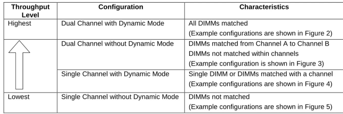
Highest Dual Channel with Dynamic Mode All DIMMs matched
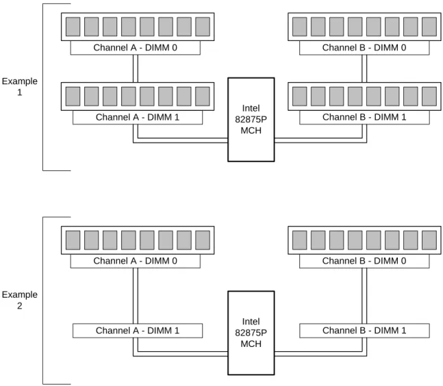
(Example configurations are shown in Figure 2) Dual Channel without Dynamic Mode DIMMs matched from Channel A to Channel B
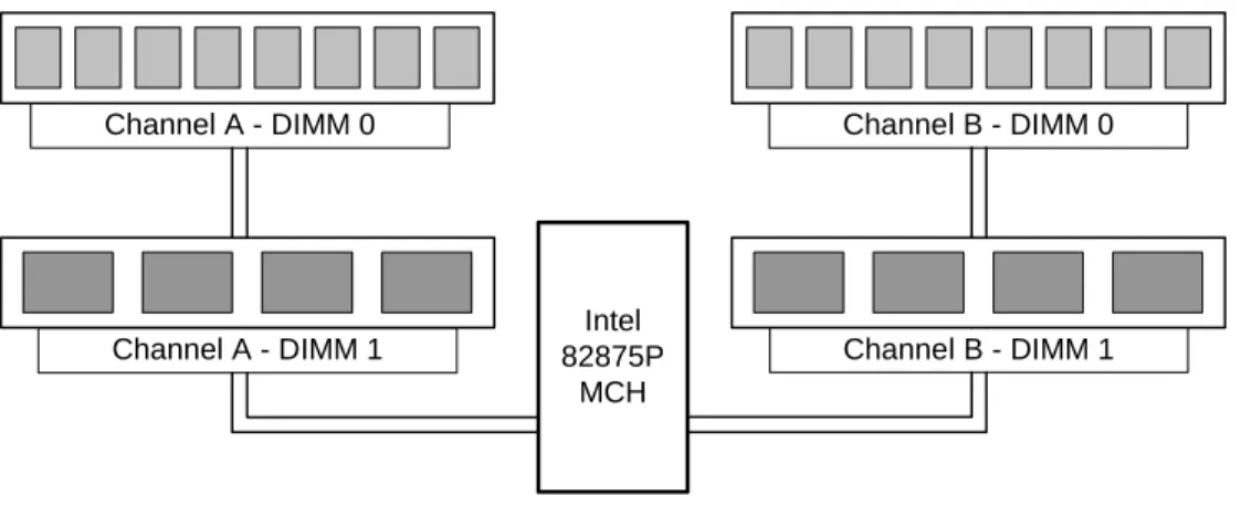
DIMMs not matched within channels (Example configuration is shown in Figure 3) Single Channel with Dynamic Mode Single DIMM or DIMMs matched with a channel
(Example configurations are shown in Figure 4)
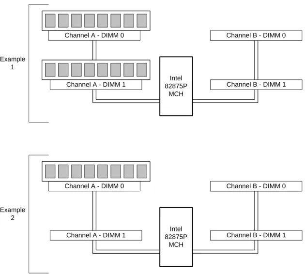
Lowest Single Channel without Dynamic Mode DIMMs not matched
Intel 82875P
MCH
Channel A - DIMM 0 Channel B - DIMM 0
Channel A - DIMM 1 Channel B - DIMM 1
Dual Channel Configuration with Dynamic Mode
(All DIMMs matched)
OM15978 Intel
82875P MCH
Channel A - DIMM 0 Channel B - DIMM 0
Channel A - DIMM 1 Channel B - DIMM 1
Example 2 Example
1
Intel 82875P
MCH
Channel A - DIMM 0 Channel B - DIMM 0
Channel A - DIMM 1 Channel B - DIMM 1
Dual Channel Configuration without Dynamic Mode
- DIMMs not matched within channel
- DIMMs match Channel A to Channel B
OM15979
Intel 82875P
MCH
Channel A - DIMM 0 Channel B - DIMM 0
Channel A - DIMM 1 Channel B - DIMM 1
Single Channel Configuration with Dynamic Mode
(Single DIMM or DIMMs matched within Channel)
OM15980 Intel
82875P MCH
Channel A - DIMM 0 Channel B - DIMM 0
Channel A - DIMM 1 Channel B - DIMM 1
Example 2 Example
1
Intel 82875P
MCH
Channel A - DIMM 0 Channel B - DIMM 0
Channel A - DIMM 1 Channel B - DIMM 1
Single Channel Configuration without Dynamic Mode
(DIMMs not matched)
OM15981 Intel
82875P MCH
Channel A - DIMM 0 Channel B - DIMM 0
Channel A - DIMM 1 Channel B - DIMM 1
Example 2 Example
1
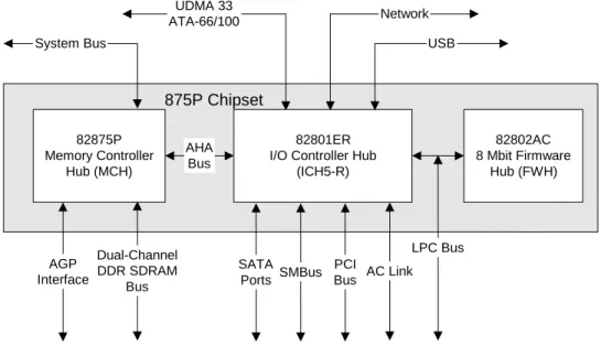
3.2 Intel 875P Chipset
The Intel 875P chipset consists of the following devices:
• Intel 82875P Memory Controller Hub (MCH) with Accelerated Hub Architecture (AHA) bus
• Intel 82801ER I/O Controller Hub (ICH5-R) with AHA bus
• Intel 82802AC (8 Mbit) Firmware Hub (FWH)
The MCH is a centralized controller for the system bus, the memory bus, the AGP bus, and the Accelerated Hub Architecture interface. The ICH5-R is a centralized controller for the Server Board S875WP1-E’s I/O paths. The FWH provides the nonvolatile storage of the BIOS. The component combination provides the chipset interfaces as shown in Figure 6.
875P Chipset
82801ER I/O Controller Hub
(ICH5-R) 82875P Memory Controller Hub (MCH) 82802AC 8 Mbit Firmware Hub (FWH) AHA Bus System Bus UDMA 33 ATA-66/100 USB AGP Interface OM15967 Network AC Link PCI Bus SMBus Dual-Channel DDR SDRAM Bus LPC Bus SATA Ports
Figure 6. Intel 875P Chipset Block Diagram
For information about Refer to
3.2.1 AGP
The AGP connector supports the following:
• 4x, 8x AGP 3.0 add-in cards with 0.8 V I/O
• 1x, 4x AGP 2.0 add-in cards with 1.5 V I/O
AGP is a high-performance interface for graphics-intensive applications, such as 3D
applications. While based on the PCI Local Bus Specification, Rev. 2.2, AGP is independent of the PCI bus and is intended for exclusive use with graphical display devices. AGP overcomes certain limitations of the PCI bus related to handling large amounts of graphics data with the following features:
• Pipelined memory read and write operations that hide memory access latency
• Demultiplexing of address and data on the bus for nearly 100 percent efficiency
✏
NOTES
• AGP 2x operation is not supported.
• Install memory in the DIMM sockets prior to installing the AGP video card to avoid interference with the memory retention mechanism.
• The AGP connector is keyed for Universal 0.8 V AGP 3.0 cards or 1.5 V AGP 2.0 cards only. Do not attempt to install a legacy 3.3 V AGP card. The AGP connector is not mechanically compatible with legacy 3.3 V AGP cards.
For information about Refer to
The AGP connector Section 5.3
3.2.2 USB
The Intel Server Board S875WP1-E supports up to six USB 2.0 ports, supports Universal Host Controller Interface (UHCI) and Enhanced Host Controller Interface (EHCI), and uses UHCI- and EHCI-compatible drivers.
The ICH5-R provides the USB controller for all ports, as shown in Figure 7. The port arrangement is as follows:
• Two ports are implemented with stacked back panel connectors, above NIC1
OM16101
82801ER I/O Controller Hub
(ICH5-R) USB USB USB USB ports [2] USB ports [2]
Back panel USB connectors above NIC1
USB ports [2]
Back panel USB connectors above NIC2
Front panel USB header Providing up to 2 USB ports
Figure 7. USB Port Configuration
✏
NOTES
• Computer systems that have an unshielded cable attached to a USB port may not meet FCC Class B requirements, even if no device is attached to the cable. Use shielded cable that meets the requirements for full-speed devices.
• Native USB 2.0 support has been tested with Windows* 2000 and Windows XP drivers and is not currently supported by any other operating system. See the Intel server board support website at http://support.intel.com/support/motherboards/server/s875wp1-e for possible driver updates for other operating systems.
For information about Refer to
The location of the USB connectors on the back panel Figure 1
The location of the front panel USB connector Figure 1
The signal names of the front panel USB header Section 5.9
Legacy USB support Section 6.4
Wake from USB Section 3.6
3.2.3 IDE
Interfaces
The ICH5-R IDE controller has two independent bus-mastering IDE interfaces that can be independently enabled. The IDE interfaces support the following modes:
• Programmed I/O (PIO): processor controls data transfer.
• 8237-style DMA: DMA offloads the processor, supporting transfer rates of up to 16 MB/sec.
• Ultra DMA: DMA protocol on IDE bus supporting host and target throttling and transfer rates of up to 33 MB/sec.
• ATA-66: DMA protocol on IDE bus supporting host and target throttling and transfer rates of up to 66 MB/sec. The ATA-66 protocol is similar to Ultra DMA and is device driver compatible.
• 100: DMA protocol on IDE bus allows host and target throttling. The ICH5-R ATA-100 logic can achieve read transfer rates up to ATA-100 MB/sec and write transfer rates up to 88 MB/sec.
✏
NOTE
ATA-66 and ATA-100 are faster timings and require a specialized 40-pin, 80-wire cable to reduce reflections, noise, and inductive coupling.
The IDE interfaces also support ATAPI devices (such as CD-ROM drives) and ATA devices using the transfer modes. The BIOS supports Logical Block Addressing (LBA) and Extended Cylinder Head Sector (ECHS) translation modes. The drive reports the transfer rate and translation mode to the BIOS.
The Server Board S875WP1-E supports Laser Servo (LS-120) diskette technology through the IDE interfaces. The BIOS supports booting from an LS-120 drive.
✏
NOTE
The BIOS will always recognize an LS-120 drive as an ATAPI floppy drive. To ensure correct operation, do not configure the drive as a hard disk drive.
For information about Refer to
The location of the IDE connectors Figure 1
The signal names of the IDE connectors Table 30
BIOS Setup program’s Boot Configuration menu Section 7.1.3.2
Drive Configuration Submenu Section 7.1.3.4
3.2.3.1 SCSI Hard Drive Activity LED Connector
The SCSI hard drive activity LED connector is a 1 x 2-pin connector that allows an add-in SCSI controller to use the same LED as the on-board IDE controller. For proper operation, this connector should be wired to the LED output of the add-in SCSI controller. The LED indicates when data is being read from, or written to, both the add-in SCSI controller and the IDE controller.
For information about Refer to
3.2.4
Real-Time Clock, CMOS SRAM, and Battery
The real-time clock provides a time-of-day clock and a multi-century calendar with alarm features. The real-time clock supports 256 bytes of battery-backed CMOS SRAM in two banks that are reserved for BIOS use.
A coin-cell battery (CR2032) powers the real-time clock and CMOS memory. When the computer is not plugged into a wall socket, the battery has an estimated life of three years. When the computer is plugged in, the standby current from the power supply extends the life of the battery. The clock is accurate to ± 13 minutes/year at 25 ºC with 3.3 VSB applied.
The time, date, and CMOS values can be specified in the BIOS Setup program. The CMOS values can be returned to their defaults by using the BIOS Setup program.
✏
NOTE
If the battery and AC power fail, custom defaults, if previously saved, will be loaded into CMOS RAM at power-on.
3.2.5
Intel 82802AC 8 Megabit Firmware Hub (FWH)
The FWH provides the following:
• System BIOS program
3.3 Serial ATA (SATA) Support
3.3.1 SATA
Interfaces
The Serial ATA controller provided by the ICH5-R offers two independent SATA ports with a theoretical maximum transfer rate of 150MB/s per port. One device can be installed on each port for a maximum of two SATA devices when using ICH5-R. Server board with order code of S875WP1 includes only two SATA ports through the ICH5-R. Server board with order code S875WP1LX includes an additional four SATA ports using an onboard Promise* Serial ATA controller, for a maximum of six SATA drives. A point-to-point interface is used for host to device connections, unlike IDE which supports a master/slave configuration and two devices per channel.
For compatibility, the underlying SATA functionality is transparent to the operating system. The SATA controller can operate in both legacy and native modes. In legacy mode, standard IDE I/O and IRQ resources are assigned (IRQ 14 and 15). In native mode, standard PCI resource steering is used. Native mode is the preferred mode for configurations using the Windows XP and Windows 2000 operating systems.
Key features include:
• Two SATA ports
• Maximum throughput of 150MB/s
• Smaller cable
✏
NOTE
• Many SATA drives use new low-voltage power connectors and require adaptors or power supplies equipped with low-voltage power connectors. For more information, see:
http://www.serialata.org/
• ATA and SATA add-in controllers may experience resource conflicts IRQ 14 and 15. Refer to the tested hardware and operating system list at (URL). In some instances, onboard SATA controller may need to be disable to use those add-in controllers.
3.3.2
SATA RAID with ICH5-R Controller
Support for RAID (Redundant Array of Independent Disks) on the two SATA ports from the ICH5-R controller is planned for a future date. See
http://support.intel.com/support/motherboards/server/S875WP1-E/ for the availability information.
3.3.3
SATA RAID with Promise Technology
*PDC20319
The Intel Server Board S875WP1LX provides additional four port Serial ATA through the use of the Promise* Technology PDC20319 ASIC. The PDC20319 SATA-150 controller contains four independent SATA channels that share a single 32-bit, 33-MHz PCI bus master interface as a multifunction device, packaged in a 144-pin LQFP.
The PDC 20319 controller supports the following features:
• Burst bus mastering and advanced packet command based scatter/gather engine to enhance overall system performance
• Built in 4 channels SATA PHY, which meets the SATA 1.0 specification and can transfer data with 1.5GHz speed
• Capable to support multiple arrays and quad master mode for dedicated SATA channel, up to four physical drive can operated at master mode.
• Quad independent data paths with read ahead and write posting supported for quad IDE channels to have high performance
• PCI interface that complies with PCI Local Bus Specification Revision 2.3 and PCI power management 1.1
• Support 48-bit LBA format for drives larger than 128GB
• 32-bit, 33-MHz bus speed and 150 MB/sec sustained transfer rate.
The Promise* PDC20319 supports SATA RAID through four SATA Channels. The RAID Engine supports advance chained packet commands for XOR and four independent ATA operations improving performance for all RAID levels. In a RAID configuration, multiple SATA hard drives are placed into one or more arrays of disks. Each array is seen as an independent disk, though the array may include upwards of two, three, or four drives. The SATA RAID can be configured as follows:
• RAID 0: Striping one to four drives.
• RAID 1: Mirroring two drives.
• RAID 10: Striping and mirroring of data concurrently (requires 4 drives)
RAID 0 configurations are used for high-performance applications, as it doubles the sustained transfer rate of its drives. RAID 1 configurations are primarily used for data protection. It creates an identical drive backup to a secondary drive. Whenever a disk write is performed, the
controller sends data simultaneously to a second drive located on a different data channel. With four drives attached to four SATA channels, one pair of striped drives can mirror themselves to another pair (RAID 10) for storage capacity and data redundancy.
3.4 I/O
Controller
The SMSC* LPC47M102 I/O Controller provides the following features:
• One serial port
• One parallel port with Extended Capabilities Port (ECP) and Enhanced Parallel Port (EPP) support
• Serial IRQ interface compatible with serialized IRQ support for PCI systems
• PS/2-style mouse and keyboard interfaces
• Interface for one 1.44 MB diskette drive
• Intelligent power management, including a programmable wake-up event interface
• PCI power management support
The BIOS Setup program provides configuration options for the I/O controller.
For information about Refer to
SMSC LPC47M172 I/O controller http://www.smsc.com
3.4.1 Serial
Ports
The Intel Server Board S875WP1-E has one 9-pin D-sub serial port connector and one 2 x 5 serial port header. The serial port A connector is located in the rear I/O area. The serial port B header is located near the main power connector. The serial ports’ NS16C550-compatible UART supports data transfers at speeds up to 115.2 kbits/sec with BIOS support. The serial ports can be assigned as COM1 (3F8h), COM2 (2F8h), COM3 (3E8h), or COM4 (2E8h).
For information about Refer to
The signal names of the serial port A connector Table 33
The location of the serial port B header Figure 1
3.4.2 Parallel
Port
The 25-pin D-Sub parallel port connector is located in the rear I/O area. In the BIOS Setup program, the parallel port can be set to the following modes:
• Output only (PC AT-compatible mode)
• Bi-directional (PS/2 compatible)
• EPP
• ECP
For information about Refer to
The location of the parallel port connector Figure 1
Setting the parallel port’s mode Table 47
3.4.3
Diskette Drive Controller
The I/O controller supports one diskette drive that is compatible with the 82077 diskette drive controller and supports both PC-AT and PS/2 modes.
For information about Refer to
The location of the diskette drive connector Figure 1
The signal names of the diskette drive connector Section 5.10
The supported diskette drive capacities and sizes Table 50
3.4.4
Keyboard and Mouse Interface
PS/2 keyboard and mouse connectors are located on the back panel. The +5 V lines to these connectors are protected with a PolySwitch* fuse circuit that, like a self-healing fuse,
reestablishes the connection after an overcurrent condition is removed.
✏
NOTE
The keyboard is supported in the bottom PS/2 connector and the mouse is supported in the top PS/2 connector. Power to the computer should be turned off before a keyboard or mouse is connected or disconnected.
The keyboard controller contains the American MegaTrends* (AMI) keyboard and mouse controller code, provides the keyboard and mouse control functions, and supports password protection for power-on/reset. A power-on/reset password can be specified in the BIOS Setup program.
For information about Refer to
The location of the keyboard and mouse connectors Section 3.4.4
3.5 Hardware Management Subsystem
The hardware management features enable the Intel Server Board S875WP1-E to be
compatible with the Wired for Management (WfM) specification 2.0. The server board complies with DMI specification 2.0 and has several hardware management features, including the following:
• Fan monitoring
• Thermal and voltage monitoring
• Chassis intrusion detection
3.5.1
Hardware Monitoring and Fan Control ASIC
The features of the hardware monitoring and fan control ASIC (Standard Microsystems SMSC EMC6D101 or equivalent) include:
• Internal ambient temperature sensor
• Two remote thermal diode sensors for direct monitoring of processor temperature and ambient temperature sensing
• Power supply monitoring of five voltages (+5 V, +12 V, +3.3 V Standby, +1.5 V, and +VCCP) to detect levels above or below acceptable values
• Thermally monitored closed-loop fan control, for four fans, that can adjust the fan speed or switch the fans on or off as needed
• SMBus interface
For information about Refer to
The Standard Microsystems SMSC EMC6D101 http://www.smsc.com
3.5.2 Fan
Monitoring
The Hardware Management ASIC provides four fan tachometer inputs. Monitoring can be implemented using LANDesk* Client Manager or third-party software.
For information about Refer to
The location of the fan connectors Figure 1
3.5.3
Chassis Intrusion and Detection
The Intel Server Board S875WP1-E supports a chassis security feature that detects if the chassis cover is removed. For the chassis intrusion circuit to function, the chassis’ power supply must be connected to AC power. The security feature uses a mechanical switch on the chassis that attaches to the chassis intrusion connector. When the chassis cover is removed the mechanical switch is in the closed position.
For information about Refer to
The location of the chassis intrusion connector Figure 1
✏
NOTE
Chassis intrusion detection may be implemented using LANDesk* Client Manager or other third-party software.
3.6 Power
Management
Power management is implemented at several levels, including:
• Software support through Advanced Configuration and Power Interface (ACPI)
• Hardware support: - Power connector - Fan connectors - LAN wake capabilities
- Instantly Available PC technology - Wake from USB
- Wake from PS/2 devices
- Power Management Event (PME#) wake-up support
3.6.1
Advanced Configuration and Power Interface (ACPI)
ACPI gives the operating system direct control over the power management and Plug and Play functions of a computer. The use of ACPI with the Intel Server Board S875WP1-E requires an operating system that provides full ACPI support. ACPI features include:
• Plug and Play (including bus and device enumeration)
• Power management control of individual devices, add-in boards (some add-in boards may require an ACPI-aware driver), video displays, and hard disk drives
• Methods for achieving less than 15-watt system operation in the standby or sleeping state
• A Soft-off feature that enables the operating system to power-off the computer
• Support for multiple wake-up events (see Table 7)
Table 5 lists the system states based on how long the power switch is pressed, depending on how ACPI is configured with an ACPI-aware operating system.
Table 5. Effects of Pressing the Power Switch If the system is in this state…
…and the power switch is
pressed for …the system enters this state Off
(ACPI S5 – Soft off)
Less than four seconds Power-on
(ACPI S0 – working state) On
(ACPI S0 – working state)
Less than four seconds Soft-off/Standby
(ACPI S1 or S3 – sleeping state) On
(ACPI S0 – working state)
More than four seconds Fail safe power-off
(ACPI S5 – Soft off) Sleep
(ACPI S1 or S3 – sleeping state)
Less than four seconds Wake-up
(ACPI S0 – working state) Sleep
(ACPI S1 or S3 – sleeping state)
More than four seconds Power-off
(ACPI S5 – Soft off)
3.6.1.1 System States and Power States
Under ACPI, the operating system directs all system and device power state transitions. The operating system puts devices in and out of low-power states based on user preferences and knowledge of how devices are being used by applications. Devices that are not being used can be turned off. The operating system uses information from applications and user settings to put the system as a whole into a low-power state.
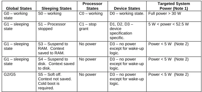
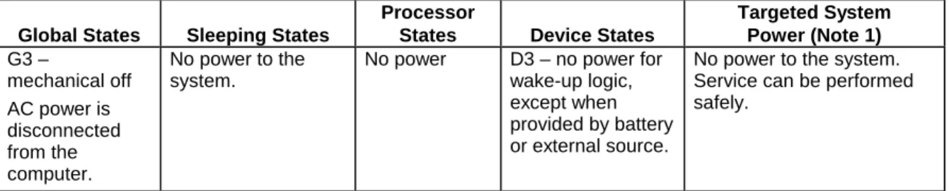
Table 6 lists the power states supported by the Server Board S875WP1-E along with the associated system power targets. See the ACPI specification for a complete description of the various system and power states.
Table 6. Power States and Targeted System Power Global States Sleeping States
Processor
States Device States
Targeted System Power (Note 1) G0 – working
state
S0 – working C0 – working D0 – working state. Full power > 30 W G1 – sleeping state S1 – Processor stopped C1 – stop grant D1, D2, D3 – device specification specific. 5 W < power < 52.5 W G1 – sleeping state S3 – Suspend to RAM. Context No power D3 – no power
except for wake-up
Global States Sleeping States
Processor
States Device States
Targeted System Power (Note 1) G3 – mechanical off AC power is disconnected from the computer. No power to the system.
No power D3 – no power for
wake-up logic, except when provided by battery or external source.
No power to the system. Service can be performed safely.
Notes:
1. Total system power is dependent on the system configuration, including add-in boards and peripherals powered
by the system chassis’ power supply.
2. Dependent on the standby power consumption of wake-up devices used in the system.
3.6.1.2 Wake-up Devices and Events
Table 7 lists the devices or specific events that can wake the computer from specific states.
Table 7. Wake-up Devices and Events These devices/events can wake up the
computer…
…from this state
LAN S1, S3, S4, S5 (Note)
Modem (back panel Serial Port A) S1, S3
PME# S1, S3, S4, S5 (Note) Power switch S1, S3, S4, S5 PS/2 devices S1, S3 RTC alarm S1, S3, S4, S5 USB S1, S3
✏
NOTE
• For LAN and PME#, S5 is disabled by default in the BIOS Setup program. Setting this option to Power On will enable a wake-up event from LAN in the S5 state.
• The use of these wake-up events from an ACPI state requires an operating system that provides full ACPI support. In addition, software, drivers, and peripherals must fully support ACPI wake events.
3.6.1.3 Plug and Play
In addition to power management, ACPI provides control information so that operating systems can facilitate Plug and Play. ACPI is used only to configure devices that do not use other hardware configuration standards. PCI devices for example, are not configured by ACPI.
3.6.2 Hardware
Support
CAUTION
Ensure that the power supply provides adequate +5 V standby current if LAN wake capabilities and Instantly Available PC technology features are used. Failure to do so can damage the power supply. The total amount of standby current required depends on the wake devices supported and manufacturing options.
The Server Board S875WP1-E provides power management hardware features, including:
• Power connector
• Fan connectors
• LAN wake capabilities
• Instantly Available PC technology
• Wake from USB
• Wake from PS/2 keyboard
• PME# wake-up support
LAN wake capabilities and Instantly Available PC technology require power from the +5 V standby line. The sections discussing these features describe the incremental standby power requirements for each.
3.6.2.1 Power Connector
ATX12V or EPS12V compliant power supplies and the Intel Server Board S875WP1-E can turn off the system power through software control. When the system receives the correct command from the operating system, the power supply removes non-standby voltages from the system. When power to the computer is interrupted by a power outage or a disconnected power cord, when power resumes, the computer returns to the power state it was in before power was interrupted (on or off). The computer’s response can be set using the After Power Failure in the BIOS Setup program’s Boot menu.
For information about Refer to
The location of the power connectors Figure 1
The signal names of the power connector Section 5.1
3.6.2.2 Fan Connectors
CAUTION
The processor fan must be connected to the processor fan connector, not to a chassis fan connector. Connecting the processor fan to a chassis fan connector may result in onboard component damage that will halt fan operation.
Table 8 summarizes the fan connector function/operation.
Table 8. Fan Connector Function/Operation
Connector Description
Processor fan • +12 V DC connection for a processor fan or active fan heatsink. • Fan is on in the S0 or S1 state.
Fan is off when the system is off or in the S3, S4, or S5 state.
• Wired to a fan tachometer input of the hardware monitoring and fan control ASIC. • Closed-loop fan control that can adjust the fan speed or switch the fan on or off as
needed.
System fans • +12 V DC connection for a system or chassis fan. • Fan is on in the S0 or S1 state.
Fan is off when the system is off or in the S3, S4, or S5 state.
• Wired to a fan tachometer input of the hardware monitoring and fan control ASIC. • Closed-loop fan control that can adjust the fan speed or switch the fan on or off as
needed.
For information about: Refer to:
The location of the fan connectors Figure 1
The signal names of the fan connectors Section 5.13.1
3.6.2.3 LAN Wake Capabilities
CAUTION
For LAN wake capabilities, the +5 V standby from the power supply must be capable of providing adequate +5 V standby current. Failure to provide adequate standby current when implementing LAN wake capabilities can damage the power supply.
LAN wake capabilities enable remote wake-up of the computer through a network. The LAN subsystem PCI bus network adapter monitors network traffic at the Media Independent
Interface. Upon detecting a Magic Packet* frame, the LAN subsystem asserts a wake-up signal that powers up the computer. Depending on the LAN implementation, the server board
S875WP1-E supports LAN wake capabilities with ACPI in the following ways:
• PCI bus PME# signal for PCI 2.2 compliant LAN designs
3.6.2.4 Instantly Available PC Technology
CAUTION
For Instantly Available* PC technology, the +5 V standby from the power supply must be capable of providing adequate +5 V standby current. Failure to provide adequate standby current when implementing Instantly Available PC technology can damage the power supply. Instantly Available PC technology enables the server board S875WP1-E to enter the ACPI S3 (Suspend-to-RAM) sleep-state. While in the S3 sleep-state, the server will appear to be off (the power supply is off, and the front panel LED is amber if dual colored, or off if single colored.) When signaled by a wake-up device or event, the system quickly returns to its last known wake state. Table 7 lists the devices and events that can wake the computer from the S3 state. The server board supports the PCI Bus Power Management Interface Specification. Add-in boards that also support this specification can participate in power management and can be used to wake the computer.
The use of Instantly Available PC technology requires operating system support and PCI 2.2 compliant add-in cards and drivers.
3.6.3
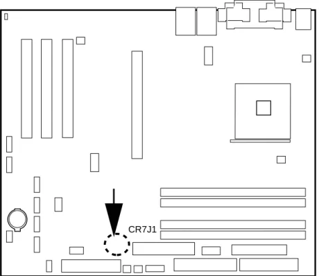
Standby Power (+5 V) Indicator LED
The standby power indicator LED (CR7J1) shows that power is still present even when the computer appears to be off. Figure 8 shows the location of the standby power indicator LED.
CAUTION
If AC power has been switched off and the standby power indicator is still lit, disconnect the power cord before installing or removing any devices connected to the board. Failure to do so could damage the board and any attached devices.
TP00185
CR7J1
Figure 8. Location of the Standby Power Indicator LED (CR7J1)
3.6.3.1 Wake from USB
USB bus activity wakes the computer from an ACPI S1 or S3 state.
✏
NOTE
Wake from USB requires the use of a USB peripheral that supports it.
3.6.3.2 Wake from PS/2 Devices
PS/2 device activity wakes the computer from an ACPI S1 or S3 state.
3.6.3.3 PME# Wake-up Support
When the PME# signal on the PCI bus is asserted, the computer wakes from an ACPI S1, S3, S4, or S5 state (with Wake on PME enabled in BIOS).
3.7 Clock Generation and Distribution
All buses on the S875WP1-E baseboard operate using synchronous clocks.Clock
synthesizer/driver circuitry on the baseboard generates clock frequencies and voltage levels as required, including the following:
• 100/133-MHz at 2.5 V & 3.3 V logic levels: For the mPGA478 socket, the MCH, and the ITP port.
• 66 MHz at 3.3 V logic levels: For the MCH and the AGP clocks.
• 33.3 MHz at 3.3 V logic levels: For the PCI slots and devices.
• 14.318 MHz at 3.3V logic levels: ICH5-R and Super I/O clocks. The synchronous clock sources on the S875WP1-E baseboard are:
• 100/133-MHz host clock generator for processor, MCH, Memory DIMMs, and the ITP.
• 66-MHz clock for MCH and the AGP clocks.
• 48-MHz clock for USB.
• 33.3-MHz PCI reference clock.
• 14.318 MHz ICH5-R and Super I/O clocks.
The S875WP1-E baseboard also provides asynchronous clock generators:
• 25-MHz clocks for the embedded network interface controllers.
• 29.498928-MHz clock for the embedded video controller.
• 20-MHz clock for the Promise PDC20319 controller.
• 32-KHz clock for the RTC.
3.8 PCI I/O Subsystem
The primary I/O bus for the Intel Server Board S875WP1-E is PCI, with one independent PCI bus. The PCI bus complies with the PCI Local Bus Specification, Rev 2.2. The PCI bus is directed through the Intel 82801ER I/O Controller Hub (ICH5-R). The table below lists the characteristics of the PCI bus.
Table 9. PCI Bus Characteristics
Voltage Width Speed Type Comments
3.8.1
32-bit, 33-MHz PCI Subsystem
All 32-bit, 33-MHz PCI I/O for the Intel Server Board S875WP1-E is directed through the Intel 82801ER I/O Controller Hub (ICH5-R). The PCI bus supports the following embedded devices and connectors:
• 2D/3D Graphics Accelerator: ATI Rage XL Video Controller
• SATA controller: Promise Technology PDC20319
• Three PCI Slots
Each of the embedded devices listed above will be allocated a GPIO to disable the device.
3.8.1.1 Device IDs (IDSEL)
Each device under the PCI hub bridge has its IDSEL signal connected to one bit of AD[31:16], which acts as a chip select on the PCI bus segment in configuration cycles. This determines a unique PCI device ID value for use in configuration cycles. The following table shows each IDSEL value for the PCI bus devices and the corresponding device description.
Table 10. PCI Bus Configuration IDs
IDSEL Value Device
16 PCI slot 1 (closest to AGP connector)
17 PCI slot 2 (middle slot)
18 PCI slot 3 (closest to left edge of board)
22 ATI Rage XL Video Controller
23 ATA-100 controller Promise Technology PDC20319
3.8.2 Video
Controller
The Intel Server Board S875WP1-E provides an ATI Rage XL PCI graphics accelerator, along with 8 MB of video SDRAM and support circuitry for an embedded SVGA video subsystem. The ATI Rage XL chip contains a SVGA video controller, clock generator, 2D and 3D engine, and RAMDAC in a 272-pin PBGA.
The SVGA subsystem supports a variety of modes, up to 1600 x 1200 resolution in 8/16/24/32 bpp modes under 2D, and up to 1024 x 768 resolution in 8/16/24/32 bpp modes under 3D. It also supports both CRT and LCD monitors up to 100 Hz vertical refresh rate.
The server board provides a standard 15-pin VGA connector and supports disabling of the on-board video through the BIOS Setup menu or when a plug-in video card is installed in the AGP slot or any of the PCI slots.
3.8.2.1 Video Modes
The Rage XL chip supports all standard IBM VGA modes. The following table shows the 2D/3D modes supported for both CRT and LCD, as well as various display resolution, refresh rates, and color depths.
Table 11. Video Modes
S875WP1-E 2D Video Mode Support 2D Mode Refresh Rate (Hz)
8 bpp 16 bpp 24 bpp 32 bpp
640x480 60, 72, 75, 90, 100 Supported Supported Supported Supported
800x600 60, 70, 75, 90, 100 Supported Supported Supported Supported
1024x768 60, 72, 75, 90, 100 Supported Supported Supported Supported
1280x1024 43, 60 Supported Supported Supported Supported
1280x1024 70, 72 Supported – Supported Supported
1600x1200 60, 66 Supported Supported Supported Supported
1600x1200 76, 85 Supported Supported Supported –
3D Mode Refresh Rate (Hz) S875WP1-E 3D Video Mode Support with Z Buffer Enabled
640x480 60,72,75,90,100 Supported Supported Supported Supported
800x600 60,70,75,90,100 Supported Supported Supported Supported
1024x768 60,72,75,90,100 Supported Supported Supported Supported
1280x1024 43,60,70,72 Supported Supported – –
1600x1200 60,66,76,85 Supported – – –
3D Mode Refresh Rate (Hz) S875WP1-E 3D Video Mode Support with Z Buffer Disabled
640x480 60,72,75,90,100 Supported Supported Supported Supported
800x600 60,70,75,90,100 Supported Supported Supported Supported
1024x768 60,72,75,90,100 Supported Supported Supported Supported
1280x1024 43,60,70,72 Supported Supported Supported –
1600x1200 60,66,76,85 Supported Supported – –
3.8.2.2 Video Memory Interface
The memory controller subsystem of the Rage XL arbitrates requests from direct memory interface, the VGA graphics controller, the drawing coprocessor, the display controller, the video scalar, and hardware cursor. Requests are serviced in a manner that ensures display integrity and maximum CPU/coprocessor drawing performance.
3.9 Network Interface Controller (NIC) Subsystem
The Intel Server Board S875WP1-E supports two Network Interface Controllers (NICs), one that runs at 10/100Mb and is based on the Intel 82562ET NIC and the other that runs at one gigabit and is based on the Intel 82547EI NIC. When looking at the rear of the chassis, the gigabit NIC is at the left (closest to the video port) and the 10/100Mb NIC is at the right. The Intel Server Board S875WP1-E supports independent disabling of the two NIC controllers using the BIOS Setup menu.
The NIC subsystem consists of the following:
• Intel 82801ER ICH5-R device with an integrated LAN Media Access Controller (MAC)
• Intel 82547EI Platform LAN Connect (PLC) device for 10/100/1000 Mbits/sec Ethernet LAN connectivity
• RJ-45 LAN connector with integrated status LEDs
The 82562ET is controlled by the ICH5 and supports the following features:
• Integrated IEEE 802.3 10Base-T and 100Base-TX compatible PHY
• IEEE 802.3u auto-negotiation support
• Full duplex support at both 10 Mbps and 100 Mbps operation
• Low power +3.3 V device with reduced power in unplugged mode and automatic detection of unplugged mode
• 3-port LED support
The 82547EI is controlled by the CSA interface off of the MCH and supports the following features:
• Basic 10/100/1000 Ethernet LAN connectivity
• Integrated Gigabit Ethernet Media Access Control (MAC) and physical layer (PHY)
• IEEE 802.3 10BASE-T/100BASE-TX/1000BASE-T compliant physical layer interface
• IEEE 802.3ab Auto-Negotiation support
• Low power (less than 350mW in active transmit mode)
• Reduced power in “unplugged mode” (less than 50mW)
• Automatic detection of “unplugged mode”
• Communication Streaming Architecture (CSA) port provides higher throughput and lower latencies resulting in up to 30% higher bus throughput (up to wire speed)
• Full device driver compatibility
• Programmable transit threshold
• Configuration EEPROM that contains the MAC address
Additional features of the NIC subsystem include:
• PCI bus master interface
• CSMA/CD protocol engine
• PCI power management - Supports ACPI technology - Supports LAN wake capabilities
3.9.1
RJ-45 LAN Connectors with Integrated LEDs
Two LEDs are built into each RJ-45 LAN connector (as shown in Figure 9). For the 82562ET NIC, the yellow LED indicates a link to the LAN and the green LED indicates the connection speed. Table 12 describes the LED states when the board is powered up and the 82562ET 10/100 Ethernet LAN subsystem is operating.
Table 12. 10/100 Ethernet LAN Connector LEDs
LED Color LED State Indicates
Off 10 Mbit/sec data rate is selected.
Green (left
LED) On 100 Mbit/sec data rate is selected.
Off LAN link is not established.
On (steady state) LAN link is established. Yellow
(right LED)
On (brighter and pulsing) The computer is communicating with another computer on the LAN.
Table 13 describes the LED states when the board is powered up and the 10/100/1000 Mbits/sec LAN subsystem is operating.
Green LED Green/Orange LED
OM15977
Figure 9. LAN Connector LED Locations Table 13. 10/100/1000 LAN Connector LED States
4. Maps and Interrupts
In this section, Table 14 describes the system memory map, Table 15 shows the I/O map, Table 16 lists the DMA channels, Table 17 defines the PCI configuration space map, and Table 18 describes the interrupts.
4.1 Memory
Map
Table 14. System Memory Map Address Range (decimal) Address Range (hex) Size Description 1024 K - 4194304 K 100000 - FFFFFFFF 4095 MB Extended memory 960 K - 1024 K F0000 - FFFFF 64 KB Runtime BIOS
896 K - 960 K E0000 - EFFFF 64 KB Reserved
800 K - 896 K C8000 - DFFFF 96 KB Available high DOS memory (open to the PCI bus)
640 K - 800 K A0000 - C7FFF 160 KB Video memory and BIOS
639 K - 640 K 9FC00 - 9FFFF 1 KB Extended BIOS data (movable by memory manager
software)
512 K - 639 K 80000 - 9FBFF 127 KB Extended conventional memory
0 K - 512 K 00000 - 7FFFF 512 KB Conventional memory
4.2 I/O
Map
Table 15. I/O Map
Address (hex) Size Description
0000 - 00FF 256 bytes Used by the Server Board S875WP1-E. Refer to the ICH5-R data
sheet for dynamic addressing information.
0170 - 0177 8 bytes Secondary IDE channel
01F0 - 01F7 8 bytes Primary IDE channel
0228 - 022F (Note 1) 8 bytes LPT3
0278 - 027F (Note 1) 8 bytes LPT2
02E8 - 02EF (Note 1) 8 bytes COM4/video (8514A)
02F8 - 02FF (Note 1) 8 bytes COM2
0376 1 byte Secondary IDE channel command port
0377, bits 6:0 7 bits Secondary IDE channel status port
0378 - 037F 8 bytes LPT1
03B0 - 03BB 12 bytes Intel 82875P MCH
03C0 - 03DF 32 bytes Intel 82875P MCH
03E8 - 03EF 8 bytes COM3
03F0 - 03F5 6 bytes Diskette channel 1
03F6 1 byte Primary IDE channel command port
Address (hex) Size Description
04D0 - 04D1 2 bytes Edge/level triggered PIC
LPTn + 400 8 bytes ECP port, LPTn base address + 400h
0CF8 - 0CFB (Note 2) 4 bytes PCI configuration address register
0CF9 (Note 3) 1 byte Reset control register
0CFC - 0CFF 4 bytes PCI configuration data register
FFA0 - FFA7 8 bytes Primary bus master IDE registers
FFA8 - FFAF 8 bytes Secondary bus master IDE registers
Notes:
1. Default, but can be changed to another address range 2. Dword access only
3. Byte access only
4.3 DMA
Channels
Table 16. DMA Channels DMA Channel
Number
Data Width System Resource
0 8 or 16 bits Open
1 8 or 16 bits Parallel port
2 8 or 16 bits Diskette drive
3 8 or 16 bits Parallel port (for ECP or EPP)
4 8 or 16 bits DMA controller
5 16 bits Open
6 16 bits Open
4.4 PCI Configuration Space Map
Table 17. PCI Configuration Space Map Bus
Number (hex)
Device Number (hex)
Function
Number (hex) Description
00 00 00 Memory controller of Intel 82875P component
00 01 00 Host to AGP bridge (virtual P2P)
00 1E 00 Hub link to PCI bridge
00 1F 00 Intel 82801ER ICH5-R PCI-to-LPC bridge
00 1F 01 IDE controller
00 1F 03 SMBus controller
00 1F 05 AC ’97 audio controller
00 1F 06 AC ’97 modem controller (optional)
00 1D 00 USB UHCI controller 1
00 1D 01 USB UHCI controller 2
00 1D 02 USB UHCI controller 3
00 1D 07 EHCI controller
01 00 00 AGP add-in card
02 08 00 LAN controller
02 00 00 PCI bus connector 1
02 01 00 PCI bus connector 2
02 02 00 PCI bus connector 3
02 03 00 PCI bus connector 4
02 04 00 PCI bus connector 5
4.5 Interrupts
The interrupts can be routed through the Advanced Programmable Interrupt Controller (APIC) portion of the ICH5-R component. The APIC is supported in Windows 2000 Server and Windows XP and supports a total of 24 interrupts.
Table 18. Interrupts
IRQ System Resource
NMI I/O channel check
0 Reserved, interval timer
1 Reserved, keyboard buffer full
2 Reserved, cascade interrupt from slave PIC
3 COM2 (Note 1)
4 COM1 (Note 1)
5 LPT2 (Plug and Play option)/User available
6 Diskette drive
7 LPT1 (Note 1)
8 Real-time clock
9 Reserved for ICH5-R system management bus
10 User available
11 User available
12 Onboard mouse port (if present, else user available)
13 Reserved, math coprocessor
14 Primary IDE (if present, else user available)
15 Secondary IDE (if present, else user available)
16 USB UHCI controller 1 (through PIRQA)
17 User available (through PIRQB)
18 ICH5-R USB controller 3 (through PIRQC)
19 ICH5-R USB controller 2 (through PIRQD)
20 ICH5-R LAN (through PIRQE)
21 User available (through PIRQF)
22 User available (through PIRQG)
23 ICH5-R USB 2.0 EHCI controller/User available (through PIRQH)
Notes:
4.6 PCI Interrupt Routing Map
This section describes interrupt sharing and how the interrupt signals are connected between the PCI bus connectors and onboard PCI devices. The PCI specification specifies how interrupts can be shared between devices attached to the PCI bus. In most cases, the small amount of latency added by interrupt sharing does not affect the operation or throughput of the devices. In some special cases where maximum performance is needed from a device, a PCI device should not share an interrupt with other PCI devices. Use the following information to avoid sharing an interrupt with a PCI add-in card.
PCI devices are categorized as follows to specify their interrupt grouping:
• INTA: By default, all add-in cards that require only one interrupt are in this category. For almost all cards that require more than one interrupt, the first interrupt on the card is also classified as INTA.
• INTB: Generally, the second interrupt on add-in cards that require two or more interrupts is classified as INTB. (This is not an absolute requirement.)
• INTC and INTD: Generally, a third interrupt on add-in cards is classified as INTC and a fourth interrupt is classified as INTD.
The ICH5-R has eight programmable interrupt request (PIRQ) input signals. All PCI interrupt sources either onboard or from a PCI add-in card connect to one of these PIRQ signals. Some PCI interrupt sources are electrically tied together on the Server Board S875WP1-E and therefore share the same interrupt. Table 19 shows an example of how the PIRQ signals are routed.
For example, using Table 19 as a reference, assume an add-in card using INTB is plugged into PCI bus connector 3. In PCI bus connector 3, INTB is connected to PIRQA, which is already connected to the Promise PDC20319 Controller. The add-in card in PCI bus connector 3 now shares an interrupt with the onboard interrupt source.
Table 19. PCI Interrupt Routing Map
ICH5-R PIRQ Signal Name PCI Interrupt Source
PIRQA PIRQB PIRQC PIRQD PIRQE PIRQF PIRQG PIRQH
AGP connector INTA INTB
PCI bus connector 1 INTF INTG INTH INTE
PCI bus connector 2 INTG INTF INTE INTH
PCI bus connector 3 INTB INTC INTD INTA
LAN_10/100 INTE
ATI Rage XL INTE
Promise PD20319 Controller INTB
✏
NOTE
In PIC mode, the ICH5-R can connect each PIRQ line internally to one of the IRQ signals (3, 4, 5, 6, 7, 9, 10, 11, 12, 14, and 15). Typically, a device that does not share a PIRQ line will have a unique interrupt. However, in certain interrupt-constrained situations, it is possible for two or more of the PIRQ lines to be connected to the same IRQ signal. See Table 18 for the allocation of PIRQ lines to IRQ signals in APIC mode.