Composition Dependence of Pd
Ag Alloy Proton Injection Layer
on Optical Switching Properties of Electrochromic Switchable Mirror
Kazuki Tajima
+, Yasusei Yamada, Masahisa Okada and Kazuki Yoshimura
Material Research Institute for Sustainable Development, National Institute of Advanced Industrial Science and Technology, Nagoya 463-8560, Japan
We fabricated electrochromic switchable mirror glass with a PdAg alloy proton injection layer to investigate the relationship between the composition of the proton injection layer and the optical switching properties, in an attempt to reduce the cost and the amount of palladium used in the fabrication of these devices. The composition of the layer was easily controlled by co-sputtering of palladium and silver metal targets with various power ratios. A device with a Pd86Ag14layer showed the maximum transmittance in the transparent state, and similar switching speed between the reflective and transparent states to a palladium-only reference device. Changing the silver content in the layer effectively controlled the reflectance of the device. The maximum reflectance in the reflective state increased with increasing silver content, due to the high reflectance of silver. However, the maximum transmittance in the transparent state decreased, and the high silver content prevented smooth switching of the device. In this work, although Pd86Ag14displayed the best properties as a proton injection layer, the performance was insufficient for commercial use. Therefore, more suitable fabrication conditions and proton injection materials will be the subject of future investigation.
[doi:10.2320/matertrans.M2011177]
(Received June 10, 2011; Accepted December 26, 2011; Published February 15, 2012)
Keywords: electrochromic, switchable mirror, thinfilm, sputtering, proton, optical properties, X-ray photoelectron spectroscopy
1. Introduction
The environmental load in houses, buildings, automobiles, airplanes, and trains must be significantly reduced if human life is to be sustainable in the long-term future. Several types of energy-saving windows have been developed for this purpose, such as double-glazing and low-emission glass, which have come into widespread use. However, these windows reduce incoming solar radiation by a constant factor, thus limiting their heat reduction performance and usefulness. Recently, switchable mirror materials have been developed which can change between transparent and reflective states as a result of hydrogenation and dehydrogen-ation of thin films.13)When these materials are adapted to be used in conventional windows, the inflow of heat into a building can be controlled effectively, by reflecting solar radiation.
Our research has focused on investigating and developing electrochromic switchable mirrors for energy-saving window applications.47)A typical device has a multilayer Mg
80Ni20/
Pd/Al/Ta2O5/WO3/indium-tin oxide (ITO) structure on a
glass substrate. The layers function as an optical switching layer, a proton injector, a buffer, a solid electrolyte, an ion storage layer, and a transparent conductor, respectively. The initial surface state of the device is the mirrored reflective (metallic) state. When a voltage is applied between the Mg80Ni20and ITO layers, protons from the ion storage layer
move into the Mg80Ni20 optical switching layer, forming
transparent MgH2 and Mg2NiH4 hydrides. In our previous
work, we attempted to develop more suitable proton injection layers for electrochromic devices from the viewpoint of practical application, in order to lower the cost and save material resources.8)The relationship between the thickness
of the palladium proton injection layer and the optical switching properties of the device was investigated. A
palladiumsilver (PdAg) alloy thin film with Pd92Ag8
composition was chosen. This alloy film is well known as a hydrogen permeation membrane due to the high solubility and diffusivity of hydrogen and its isotopes in the lattice.914)
However, the reduction of the amount of palladium in the layer was minimal. For practical use, it is important to reduce the amount of palladium even further. Therefore, here we fabricate a PdAg alloy proton injection layer with various compositions by dc co-sputtering of palladium and silver metal targets. The optical switching properties of these devices were investigated.
2. Experimental
2.1 Device fabrication
A commercially available WO3/ITO/glass substrate (30 mm©30 mm©1.1 mm, Geomatec Co.) was used. Ta2O5 (thickness: 400 nm) was deposited on top of this by
reactive dc magnetron sputtering with a sputtering power of 70 W, in a mixture of argon and oxygen with a gas flow volume ratio of 7 : 1, under a working pressure of 0.7 Pa. Protons were supplied across the Ta2O5 layer to the WO3
film, by dipping in 0.5 mol·m¹3 sulfuric acid solution
electrochemically. Aluminum (thickness: 2 nm) was then deposited by dc magnetron sputtering with a sputtering power of 52 W under a working pressure of 0.65 Pa. A Pd Ag alloy proton injection layer under a working pressure of 1.2 Pa. The thickness of the layer was fixed to 4 nm monitored by sputtering time, power and quartz crystal unit. The composition was controlled by the co-sputtering power ratio of the palladium and silver targets. Finally, MgNi (thickness: 40 nm) was deposited by co-sputtering magne-sium and nickel from metal targets. The sputtering power ratio of Mg to Ni was adjusted to 1.88 in order to deposit a Mg80Ni20layer, which has already been shown to have good
optical switching properties.4) The working pressure was
1.2 Pa. All processes were carried out at room temperature.
2.2 Characterization
The surface state and chemical composition of the proton injection layer were characterized by X-ray photoelectron spectroscopy (XPS; Sigma Probe, Thermo Scientific) with argon sputter etching. The optical switching properties of the devices were measured with a laser diode (=670 nm) together with a silicon photodiode. The electrodes were connected with the Mg80Ni20 and ITO thin films, and a
voltage of «5 V was applied to change the state of the devices. The surface morphology of the device was evaluated by atomic force microscopy (AFM) with optical microscopy (VN-8000, Keyence Co.).
3. Results and Discussion
3.1 XPS analysis of the PdAg proton injection layer
We confirmed the surface state of the PdAg proton injection layer by XPS analysis on samples in which the surface Mg80Ni20 optical switching layer was not deposited.
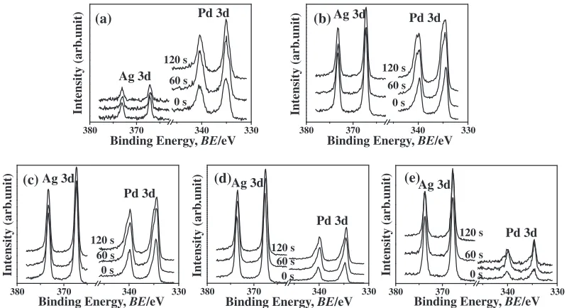
Figure 1 shows XPS spectra of the Pd 3d and Ag 3d signals for as-prepared PdAg films. The etching time t=0 s corresponds to the sample surface. The inside of the films was evaluated by argon sputter etching. The times of 60 and 120 s mean the etching time. The Pd 3d5/2 metallic peak
position is located at around 335 eV, and the Ag 3d5/2
metallic peak position is at approximately 368 eV.15)A peak
shift originated from typical compound with contamination was not observed by argon sputter etching. This result indicates that the PdAg films had uniform compositions without the formation of other compound. Figure 1(a) shows the XPS spectrum for the PdAg thin film fabricated by the sputtering powers 30 W (palladium) and 5 W (silver). Figures 1(b) to 1(e) show results for palladium and silver sputtering power ratios of 30 : 15, 30 : 30, 15 : 30, and 5 : 30, respectively. When the silver content in the layer was increased and the palladium content in the layer was decreased, the Ag 3d peak intensity increased, and the Pd 3d peak intensity decreased. Therefore, varying the sputtering
power of palladium and silver deposition can effectively control the elemental composition of the layer. The chemical composition of the PdAg layers was estimated from Fig. 1 using Avantage of computer software for XPS.
Figure 2 shows the relationship between the power ratio and the concentration of palladium in the layer, as estimated by XPS analysis. The sputtering power ratio of 1 corresponds to sputtering of a palladium metal target with a power of 30 W. The ratio of 0.86 corresponds to a layer fabricated by co-sputtering of palladium and silver with powers of 30 and 5 W, respectively. The relationship between sputtering power ratio and concentration of palladium is linear. The calculated results show the chemical composition of the layer, and the composition was rewritten as a relationship of PdAg. For example, a layer with Pd67Ag33 composition was fabricated
using a power ratio of 0.67. To summarize, the composition of the layer could be simply controlled by varying the sputtering powers of palladium and silver.
3.2 Device properties
We investigated the optical switching properties of devices with various PdAg proton injection layer compositions
(c) (e)
(a)
380 370 340 330
Intensity (arb
.unit)
Binding Energy, BE/eV 380 370 340 330
Intensity (arb
.unit)
Binding Energy, BE/eV
380 370 340 330
Intensity (arb
.unit)
Binding Energy, BE/eV
(b)
380 370 340 330 Binding Energy, BE/eV
Intensity (arb
.unit)
(d)
380 370 340 330
Intensity (arb
.unit)
Binding Energy, BE/eV Pd 3d
Ag 3d
0 s 60 s 120 s
0 s 60 s 120 s
0 s 60 s 120 s
0 s 60 s 120 s
0 s 60 s 120 s Pd 3d
Ag 3d
Pd 3d
Ag 3d
Ag 3d
Pd 3d
Pd 3d Ag 3d
Fig. 1 XPS Pd 3d and Ag 3d spectra of PdAg layers, fabricated by co-sputtering of palladium and silver metal targets. The Pd/Ag power ratios were (a) 30/5, (b) 30/15, (c) 30/30, (d) 15/30, and (e) 5/30.
0.0 0.1 0.2 0.3 0.4 0.5 0.6 0.7 0.8 0.9 1.0 0
10 20 30 40 50 60 70 80 90 100
Pd Concentration (mol%)
Sputtering Power Ratio, Pd/Ag
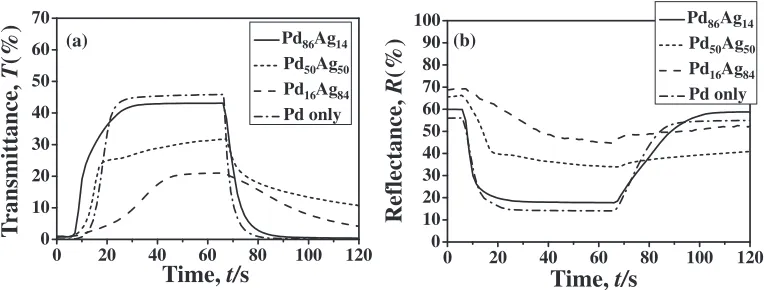
[image:2.595.99.500.69.286.2] [image:2.595.325.528.333.482.2](Fig. 3). Specifically, we measured the properties of devices with compositions of Pd86Ag14, Pd50Ag50, and Pd16Ag84. The
results were compared to a reference device containing a pure Pd layer. Figure 3(a) shows the change in transmittance, and Fig. 3(b) shows the change in reflectance under an applied voltage of«5 V. For example, when a voltage was applied to the reference device at 5 s, the transmittance changed from the reflective state (0.1%) to the transparent state (44%). The reflectance changed from 57 to 15%. When the polarity of the voltage was reversed at 65 s, the device changed back to the reflective state. The device with a Pd86Ag14proton injection
layer had a transmittance of 41% in the transparent state, which is similar to the reference device. When the silver content in the PdAg alloy thinfilm increased, the maximum reflectance in the reflective state increased to 69% (Pd16Ag84). However, the maximum transmittance in the
transparent state decreased to 20%. These results appear to be related to the high reflectance of silver.16) Furthermore, the reversal time (the time taken to switch from the transparent state to the reflective state) increased with increasing silver content. Indeed, devices with Pd50Ag50 and Pd16Ag84 layers
were not able to change from the reflective state to the fully transparent state, suggesting that the Mg80Ni20 optical
switching layer remains partially dehydrogenated in this case. This in turn suggests that a proton injection layer including high silver content is not suitable to inject protons into the optical switching layer. A reference device using only a silver thinfilm did not show any optical switching properties. For commercial use, high reflectance in the reflective state is required to control solar radiation of heat effectively. However, in this case the optical switching range between transmittance and reflectance was reduced when silver content in the proton injection layer increased. Therefore, the optical design of the multilayer structure of the device should be optimized, with suitable fabrication conditions. Moreover, when the device has crystalline layers, it is difficult to observe the optical switching properties because amorphous layers are needed for moving protons in the layer smoothly by switching. The details of the crystallinity of layer will be investigated by using transmission electron microscope in future work.
We also evaluated the surface of the device in relation to the optical switching performance. Figure 4 shows AFM
topography images of as-prepared devices with various Pd Ag layer compositions. Each as-prepared device had a relatively smooth surface. For example, the device containing a Pd86Ag14layer had a surface roughness ofRa=1.8 nm, and
a grain size of around 50 nm, as shown in Fig. 4(a). As the silver content in the layer increased, the surface of the device showed only slightly different morphology. In particular, the device with a Pd50Ag50 layer had afiner grain structure, and
a surface roughness of Ra=2.2 nm, as shown in Fig. 4(b).
Conversely, the reference device with a pure Pd layer had a slightly larger grain structure than that of other devices, with a surface roughness of Ra=1.6 nm, as shown in Fig. 4(d).
This result indicates that although the addition of silver induces a finer grain structure, there may be a limit to this effect.
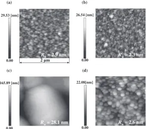
The devices were also evaluated by AFM after several switching cycles of the optical state. Figure 5 shows the surfaces of switched devices with various PdAg composi-tions. Each device was switchedfive times; one cycle being the same as the measurement conditions described in Fig. 3. The surface roughness of the devices increased after five switching cycles, as shown in Figs. 5(a), 5(b), and 5(d). The surface roughness was measured as Ra=2.9 nm, Ra=
2.3 nm, andRa=2.6 nm, for switched devices with Pd86Ag14
and Pd50Ag50 layers, and the Pd reference device,
respec-tively. Conversely, a peculiar surface structure change was observed in the switched device with a Pd16Ag84layer, with a
surface roughness of Ra=28.1 nm, as shown in Fig. 5(c).
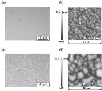
This structural change was evaluated in more detail in Fig. 6, which shows a comparison of optical and AFM topography images for the Pd16Ag84device. The as-prepared device had a
smooth surface and it did not show any typical structure, as shown in Fig. 6(a). However, after five switching cycles, a distinct surface change was observed on the Pd16Ag84device,
as shown in Fig. 6(c), and many large surface features were found, as observed by AFM [Fig. 6(d)]. It is presumably due to this surface change that the device with high silver content in the proton injection layer displayed strange optical switching properties. To solve this problem, it will be necessary to develop more suitable methods to deposit the proton injection layer.
In our previous work, the device properties were affected by temperature and relative humidity of the local
environ-0 20 40 60 80 100 120
0 10 20 30 40 50 60 70
T
ransmittance,
T
(%)
Time, t/s
Pd86Ag14 Pd50Ag50 Pd16Ag84 Pd only
0 20 40 60 80 100 120
0 10 20 30 40 50 60 70 80 90
100 Pd86Ag14
Pd50Ag50
Pd16Ag84 Pd only
Reflectance,
R
(%)
Time, t/s
(a) (b)
[image:3.595.108.490.71.216.2]ment.17) Therefore, it is clear that the optical switching properties are closely related to a variety of factors. In future work, we will investigate suitable fabrication conditions for the proton injection layer, for example, by varying the composition, thickness, structure, sputtering power, and working pressure in order to realize improved devices. Moreover, alternative materials will be researched and adapted to be used as proton injection layers for electro-chromic devices.
4. Conclusions
PdAg alloy thin films with varying composition were deposited by co-sputtering of palladium and silver metal targets, in order to fabricate proton injection layers for electrochromic devices. The composition of the layer was linearly related to the palladium and silver sputtering power ratio. For example, a Pd50Ag50 layer was fabricated using
sputtering powers of 30 W for both palladium and silver
Ra= 2.3 nm
0.00 26.54 [nm]
0.00
165.89 [nm] 22.08[nm]
Ra= 28.1 nm Ra= 2.6 nm
(b)
(d) (c)
(a)
2 µm 0.00
29.53 [nm]
Ra= 2.9 nm
0.00
Fig. 5 AFM images of surface of the devices afterfive switching cycles. (a) Pd86Ag14, (b) Pd50Ag50, (c) Pd16Ag84, and (d) Pd only.
Ra= 2.2 nm 0.00
19.75 [nm]
0.00 19.41 [nm]
0.00 11.27 [nm]
Ra= 2.1 nm Ra= 1.6 nm
(b)
(d) (c)
(a)
2 µm 0.00
16.25 [nm]
Ra= 1.8 nm
[image:4.595.156.441.71.327.2] [image:4.595.151.447.378.640.2]targets. The optical switching properties of electrochromic devices using these proton injection layers were also evaluated. A device containing a Pd86Ag14 layer had a
transmittance of 41% in the transparent state, and the switching speed between the reflective and transparent states was similar to a reference device with a pure Pd proton injection layer. When the silver content of the PdAg layer was increased, the maximum reflectance in the reflective state increased. However, the maximum transmittance in the transparent state decreased, due to the high reflectance of silver. Furthermore, the device with high silver content in the PdAg layer showed considerably higher surface roughness and large grain size after five switching cycles. The relationship between the composition of the PdAg proton injection layer and the optical switching properties of the device was investigated in this work. However, for commercial use it is necessary to conduct further research into more suitable fabrication conditions, and to apply alternative materials to the PdAg proton injection layer.
Acknowledgment
This work was supported by KAKENHI (21760570) of Japan Society for the Promotion of Science.
REFERENCES
1) T. J. Richardson, J. L. Slack, R. D. Armitage, R. Kostecki, B. Farangis and M. D. Rubin:Appl. Phys. Lett.78(2001) 30473049.
2) B. Farangis, P. Nachimuthu, T. J. Richardsona, J. L. Slacka, B. K. Meyer, R. C. C. Pereraa and M. D. Rubin:Solid State Ionic.165(2003) 309314.
3) J. L. M. van Mechelen, B. Noheda, W. Lohstroh, R. J. Westerwaal, J. H. Rector, B. Dam and R. Griessen:Appl. Phys. Lett.84(2004) 36513653.
4) K. Yoshimura, Y. Yamada and M. Okada:Appl. Phys. Lett.81(2002) 47094711.
5) Y. Yamada, K. Tajima, M. Okada, S. Bao and K. Yoshimura:Jpn. J. Appl. Phys.46(2007) 51685171.
6) K. Tajima, Y. Yamada, S. Bao, M. Okada and K. Yoshimura:Appl. Phys. Lett.91(2007) 051908-1051908-3.
7) K. Tajima, Y. Yamada, S. Bao, M. Okada and K. Yoshimura:Appl. Phys. Lett.92(2008) 041912-1041912-3.
8) K. Tajima, Y. Yamada, M. Okada and K. Yoshimura:Thin Solid Films
519(2010) 934937.
9) Y. Sakamoto, S. Hirata and H. Nishikawa:J. Less-Common Met.88
(1982) 387395.
10) T. Ishikawa and R. B. McLellan:Acta Metall.34(1986) 18251831.
11) J. Shu, A. Adnot, B. P. A. Grandjean and S. Kaliaguine:Thin Solid Films286(1996) 7279.
12) B. McCool, G. Xomeritakis and Y. S. Lin:J. Membr. Sci.161(1999) 6776.
13) S. Tosti, L. Bettinali and V. Violante: Int. J. Hydrogen Energy 25
(2000) 319325.
14) H. D. Tonga, A. H. J. vanden Berga, J. G. E. Gardeniersa, H. V. Jansena, F. C. Gielensb and M. C. Elwenspoek:Thin Solid Films479
(2005) 8994.
15) M. L. Bosko, J. B. Miller, E. A. Lombardo, A. J. Gellman and L. M. Cornaglia:J. Membr. Sci.369(2011) 267276.
16) A. Rizzo, M. A. Tagliente, M. Alvisi and S. Scaglione:Thin Solid Films396(2001) 2935.
17) K. Tajima, Y. Yamada, M. Okada and K. Yoshimura: Sol. Energy Mater. Sol. Cell.94(2010) 17161722.
(a)
(b)
40 µm
10 µm
0.00 212.71 [nm]
R
a= 32.3 nm
(c)
(d)
2 µm
R
a= 2.1 nm
40 µm
0.00 19.41 [nm]
[image:5.595.123.468.69.378.2]