Electron Backscatter Diffraction Characterization
of Microstructure Evolution of Electroplated Copper Film
Su-Hyeon Kim, Joo-Hee Kang and Seung Zeon Han
Korea Institute of Materials Science, 531 Changwondaero, Changwon, Gyeongnam, 641-831, Korea
The microstructure evolution of electroplated copper films was characterized by electron backscatter diffraction (EBSD). Special care was taken during the preparation of the cross-sectional specimens and microstructure analysis to obtain reliable results. The film exhibited a columnar grain structure with a large fraction of twin boundaries. Annealing induced normal grain growth and caused many of the general high-angle grain boundaries to be replaced by twin boundaries, possibly by annealing twinning. [doi:10.2320/matertrans.MG200910]
(Received September 30, 2009; Accepted February 5, 2010; Published March 17, 2010)
Keywords: electron backscatter diffraction, copper film, columnar grain structure, high-angle grain boundary, twin boundary, annealing, grain growth, annealing twinning
1. Introduction
Copper film is used as a metallization material in micro-electronics. The increasing interest in copper films is driven by their large spectrum of applications in printed circuit boards, ultra large-scale integration (ULSI) metallization, and flexible electronics. The physical, mechanical, and chemical properties of polycrystalline copper films are influenced by their microstructural characteristics, such as their grain size, grain boundary characteristics, and grain orientation. The strengths of metallic films are inherently related to their grain size. Their electromigration perform-ance is influenced by their grain size, grain distribution, grain boundary misorientation and texture.1) The flexibility or
bending fatigue resistance of the copper films used for flexible printed circuit boards is strongly influenced by their microstructure evolution.2,3)The texture evolution should be
taken into consideration, because the macroscopic behavior of polycrystalline copper films depends on the orientation distribution of the crystallites. The elastic anisotropy of textured copper films can give rise to non-uniform mechan-ical properties,4,5)and their grain boundary characteristics are
influenced by their texture evolution. The microstructure of copper films grown by vapor deposition or electro-deposition can be changed by heat treatment. The modification of the grain boundary structure of copper films by recrystallization, grain growth, and twin formation during annealing can change their properties and reliability.
The microstructure evolution of copper films can be characterized by several techniques: optical and electron microscopy,6–11)focused ion beam (FIB) imaging,6,12–15)and
electron backscatter diffraction (EBSD).12,16,17) EBSD
pro-vides information on the grain size and morphology statistics and grain boundary characteristics, as well as the crystal orientation of the individual grains. There have been several studies involving the EBSD analysis of copper films,12,16,17)
but systematic studies by means of cross-sectional mapping are still lacking.18)Cross-sectional observation is essential for identifying columnar grain structures of copper films. EBSD measurement only on the film surface12,16,17)does not provide overall information throughout the thickness of the speci-mens. The cross-sectional EBSD measurement by Pantleon
et al.18)would not be guaranteed because many numbers of
the pixels remained non-indexed and the grain morphology was not identified.
In the present study, we carried out a cross-sectional EBSD analysis of electroplated copper films. Special care was taken in preparing the EBSD specimens, in order to avoid any possible artifacts of orientation measurement. A commercial flexible copper clad laminate (FCCL), where copper film was deposited on polyimide (PI) film, was used. The specimens were annealed and the effect of the annealing was inves-tigated. We characterized the grain size and grain boundary characteristics of the as-received and annealed specimens and discussed the mechanism of microstructure evolution.
2. Experimental
2.1 Specimen preparation
The specimen used in this study is a commercial FCCL which is composed of 8mm-thick electroplated copper film and 35mm-thick PI film. The as-received FCCL was cut into several coupons and they were annealed in a convection oven in an air atmosphere at 150, 200, 250 or 300C for
15 min. The annealed specimens were immersed in a nitric acid solution for several seconds to remove the surface oxide.
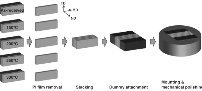
Figure 1 shows the process used for the preparation of the EBSD specimens. The mechanical polishing method was used in this study. Ion etching and FIB are frequently used, but these processes can cause thermal transformation or crystal lattice damage to temperature-sensitive and soft materials. This study employed a simple mechanical polish-ing process to obtain satisfactory surface quality. The polyimide film was completely removed by immersing the FCCL specimens in a KOH solution at 50 to 60C for about
3 h, because the non-conductive film should be removed to help eliminate charging and severe drift problems during long-term EBSD mapping. The copper films were stacked together and then inserted between two dummy copper (phosphor bronze) plates and mounted in a 25 mm diameter brass holder. The mounted specimen was mechanically ground and polished using an Allied Dualprep 3 auto-polisher in conjunction with an AP-4 power head. The specimen was
ground with silicon carbide papers and then polished with polycrystalline 3 and 1mm diamond suspensions. Final polishing was done with a 0.05mmcolloidal silica suspension with a pH of 9.8 for 30 min. During polishing, a 13N force was applied to the specimen, and the plate and holder were rotated at 120 rpm. No further treatment, such as electro-polishing, chemical etching, or conductive coating on the surface, was necessary.
2.2 EBSD measurement and analysis
For EBSD mapping, a Tescan Mira II scanning electron microscope incorporating an EDAX-TSL Hikari EBSD detector was used. The magnification of each mapping was 15,000 and the mapping speed was 180 points per second. Each pixel was 30 nm in size and hexagonal in shape. The area size of a single mapping was about 8mm30mm. A total of 9 or 10 mapping data were gathered for each specimen, giving a total mapping area for each specimen of 2,000–2,500mm2. Number of non-indexed pixels was less
than 1% of the total measured pixels and the average confidence index was 0.6 to 0.7.
TSL OIM analysis software version 5.3 was used to analyze the EBSD measurement results. Erroneous pattern indexing was corrected by a clean-up procedure consisting of single iteration grain dilation19)with the parameters of grain tolerance being 5 misorientation and a minimum grain of
two pixels. A grain was defined as a single-oriented region divided by high-angle grain boundaries (HAGB). If two neighboring pixels had a misorientation of less than or equal to 15, they were considered part of the same grain. A grain
consisting of less than five pixels was excluded from the grain size calculation. The grain size was defined as the mean intercept length using the linear intercept method. Both vertical and horizontal lines were used and the mean intercept length is defined by
d¼1=N ð1Þ
whered is the mean intercept length andNis the number of intersections per unit length of test line with the grains. The average grain size is defined as the geometric mean value of the vertical and horizontal intercept lengths using the following equation.
dav¼ ðdvdhÞ1=2 ð2Þ
wheredavis the average grain size, anddv anddhare the
vertical and horizontal intercept lengths, respectively. A twin boundary was defined as a grain boundary across which the misorientation relationship was a 60 rotation about a
h111icrystal axis.
The texture evolution was described by the area fraction of the specific crystallographic direction parallel to the normal direction of the specimen. The calculation of the area fraction was carried out within an angular tolerance of 5.
3. Results and Discussion
Figure 2 shows the cross-sectional orientation maps of the as-received and annealed copper films. ND is the normal direction and MD is the machine direction of film fabrication. The through-thickness observation of the specimen revealed that the microstructure consisted of very small grains near the interface between the copper film and the polyimide (PI) film and relatively large grains in the remaining area. Figure 3 shows the grain boundary maps of the specimens. The black, grey, and red lines indicate the HAGBs with a boundary misorientation of 15 or larger, low angle grain boundaries
(LAGB) with a boundary misorientation of 2 to 15, and
twin boundaries, respectively. The grain boundary structure of the specimen exhibited an HAGB structure with a large amount of twin boundaries. The presence of the LAGBs mainly originated from the substructure inside the grains. Twin boundaries were not as frequently found at the interface as in the remaining area.
Figure 4 shows the grain boundary misorientation histo-grams of the areas at a distance of 2mm from the Cu/PI interface toward the Cu surface. The Cu/PI interface regions were excluded from the quantitative analysis, because the grain sizes were too small and the unsolved areas were large. A large fraction of the 60 misoriented
boundaries correspond to twin boundaries, and a low fraction of LAGBs indicates that the specimens exhibit an HAGB structure. Except for the LAGBs and twin boundaries, the distribution of the boundary misorientation is close to that for randomly oriented grains, which indicates that the specimens do not have a strong texture. The presence of LAGBs does not seem to be an indication of a well-developed texture, because they were in the substructure inside the grains, as shown in Fig. 3.
Dummy attachment PI film removal
Mounting & mechanical polishing As-received
150°C
200°C
MD TD
ND
250°C
Stacking 300°C
[image:2.595.130.465.72.223.2]The grain structure of metallic films grown by electro-plating is influenced by the substrate or seed layer structure. Their epitaxial growth is responsible for the morphology and orientation of the grains near the interface. However, the microstructure in the overall region of the as-received specimen does not resemble that at the interface. This
microstructure composed of HAGBs and twin boundaries could be formed during electroplating or room temperature recrystallization right after electroplating (self annealing). The microstructure of the electrodeposits can be changed by increasing the film thickness16)and by altering the electro-plating conditions.17)
5µm
5µm
5µm (a)
(b)
(c)
(d)
(e)
5µm
5µm
Surface direction
Cu/Pi interface direction
MD
Color: ND ND
111
101 001
Fig. 2 Orientation maps of the copper films; (a) as-received, (b) annealed at 150C, (c) annealed at 200C, (d) annealed at 250C, and (e) annealed at 300C.
5µm 5µm
5µm
(a)
(b)
(c)
(d)
(e)
5µm
5µm
Surface direction
Cu/Pi interface direction
MD ND
HAGB
Twin boundary LAGB
[image:3.595.71.526.68.348.2] [image:3.595.68.531.394.664.2]Figure 2 also indicates that the annealing caused grain coarsening. We suggest that the microstructural changes caused by annealing are driven by a normal grain growth mechanism. Recrystallization did not occur even after high temperature annealing at 300C.
Table 1 shows the area fractions ofh111i,h100i, andh110i
oriented grains calculated within a 5angular deviation from
the ideal ND fiber axis. The film did not develop a strong texture and annealing also did not appear to cause any critical changes in the texture evolution.
Figure 5 shows the grain size as a function of the annealing temperature. It was found that the vertical grain size (dv) was
always larger than the horizontal grain size (dh), which
indicates that the film exhibits columnar grain structure. The microstructure characterization by surface analysis reported by other researchers12,16,17) would not be identical to that
determined by the cross-sectional measurement because the surface view shows the horizontal sectioning of the film but cannot provide any information of the vertical sectioning. Mirpuri et al.12) identified the columnar grain structure of
copper films in a FIB cross-sectional image but provided incomplete information of the microstructure evolution because EBSD mapping was carried out only on the film surface. The cross-sectional observation is essential to understand the real microstructure evolution of the electro-plated copper films.
Figure 5 also shows that the average grain size (dav)
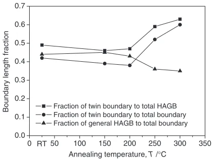
increased with increasing annealing temperature. As men-tioned previously, the increase in the grain size is driven by normal grain growth, and the driving force of grain growth is the reduction of the grain boundary energy. The grain boundary energy can be reduced by reducing the grain boundary length through grain growth. Figure 6 shows the boundary lengths of the LAGBs, total HAGBs, twin boundaries, and general HAGBs as a function of the annealing temperature. A general HAGB was defined as an HAGB excluding twin boundaries, so that a total HAGB is composed of both a general HAGB and twin boundary. General HAGBs rather than total HAGBs are more indicative of high energy grain boundaries, because the interfacial energy of coherent twin boundaries is much lower than that of the average grain boundaries in copper.20) Annealing reduced the lengths of the LAGBs, total HAGBs, and general HAGBs. The twin boundary length was not significantly changed by annealing at 150 or 200C, but increased when annealing was performed above 200C (Fig. 6). The increase in the twin boundary length caused by high temperature
Misorientation angle / °
Number fraction
0.1 0.2 0.3 0.4 0.5 0.6
10 20 30 40 50 60
(a)
Misorientation angle / °
Number fraction
0.1 0.2 0.3 0.4 0.5 0.6
10 20 30 40 50 60
(b)
Misorientation angle / °
Number fraction
0.1 0.2 0.3 0.4 0.5 0.6
10 20 30 40 50 60
(c)
Misorientation angle / °
Number fraction
0.1 0.2 0.3 0.4 0.5 0.6 (d) 0.7
10 20 30 40 50 60
(e)
Misorientation angle / °
10 20 30 40 50 60
Number fraction
0.1 0.2 0.3 0.4 0.5 0.6 0.7
[image:4.595.318.533.327.483.2]Fig. 4 Grain boundary misorientation histograms of the copper films; (a) as-received, (b) annealed at 150C, (c) annealed at 200C, (d) annealed at 250C, and (e) annealed at 300C.
Table 1 Area fractions of h111i, h100i, and h110i ND fiber texture components.
Annealing Texture component
temperature,T/C
h111i h100i h110i
Room temperature 0.017 0.011 0.015
150 0.024 0.005 0.040
200 0.025 0.013 0.028
250 0.019 0.013 0.023
300 0.020 0.020 0.033
0 50 100 150 200 250 300 350
0.3 0.4 0.5 0.6
Vertical grain size (d
v)
Horizontal grain size (dh)
Average grain size (d
av)
Grain size
d
/
µ
m
Annealing temperature, T /°C RT
[image:4.595.46.291.353.450.2]annealing is attributed to the generation of annealing twins. During grain growth, annealing twins can be formed in order to reduce the grain boundary energy.20)The reduction in the
number of general HAGBs with a relatively high grain boundary energy is mainly responsible for the reduction of the total HAGB length during high temperature annealing.
The modification of the grain boundary characteristics is shown in Fig. 7. The total boundary is composed of the LAGB and the total HAGB. Low temperature annealing at 150 or 200C did not appreciably change the fractions of twin
boundaries, HAGBs, and LAGBs. Meanwhile, high temper-ature annealing at 250 and 300C increased the fraction of
twin boundaries and decreased that of the general HAGBs. After annealing at 300C, the twin boundaries accounted for
about 60% of the total boundaries. We suggest that annealing causes many of the general HAGBs to be replaced by twin boundaries through grain growth and the formation of annealing twins.
4. Conclusion
The through-thickness EBSD analysis successfully re-vealed the columnar grain structure of the copper film electroplated on polyimide film. The grain structure of the copper film was characterized by a high angle grain boundary structure with a large fraction of twin boundaries. During annealing, the normal grain growth mechanism is responsible for the increase in the grain size and the decrease in the length of the high angle grain boundaries. During annealing at high temperatures above 250C, many of the general high angle
grain boundaries ware replaced by twin boundaries through grain growth and annealing twinning.
Acknowledgement
This work was supported by the Next Generation New Technology Development Program of the Ministry of Knowledge Economy, Korea. The authors are grateful to Hye Kyung Kim at Changwon National University for the EBSD measurements.
REFERENCES
1) C. M. Tan and A. Roy: Mater. Sci. Eng. R58(2007) 1–75. 2) T. Hatano, Y. Kurosawa and J. Miyake: J. Electron. Mater.29(2005)
611–616.
3) H. D. Merchant, M. G. Minor and Y. L. Liu: J. Electron. Mater.28
(1999) 998–1007.
4) A. Wikstro¨m and M. Nyga˚rds: Acta Mater.50(2002) 857–870. 5) Y. Tomioka and N. Yuki: J. Mater. Proc. Tech.146(2004) 228–233. 6) T. Wang, P. Lindquist, S. Erdemli, E. C. Basol, R. Zhang, C. E. Uzoh
and B. M. Basol: Thin Solid Films478(2005) 345–351.
7) L. A. Giannuzzi, P. R. Howell, H. W. Pickering and W. R. Bitler: Scr. Metall.23(1989) 1353–1358.
8) H. D. Merchant, W. C. Liu, L. A. Giannuzzi and J. G. Morris: Mater. Charact.53(2004) 335–360.
9) S. P. Hau-Riege and C. V. Thompson: Appl. Phys. Lett.76(2000) 309– 311.
10) J.-M. Paik, Y.-J. Park, M.-S. Yoon, J.-H. Lee and Y.-C. Joo: Scr. Mater.
48(2003) 683–688.
11) C. E. Murray, K. P. Rodbell and P. M. Vereecken: Thin Solid Films503
(2006) 207–211.
12) K. Mirpuri, H. Wendrock, S. Menzel, K. Wetzig and J. Szpunar: Thin Solid Films496(2006) 703–717.
13) C. Lingk, M. E. Gross and W. L. Brown: J. Appl. Phys.87(2000) 2232–2236.
14) K. B. Yin, Y. D. Xia, C. Y. Chan, W. Q. Zhang, Q. J. Wang, X. N. Zhao, A. D. Li, Z. G. Liu, M. W. Bayes and K. W. Yee: Scr. Mater.58(2008) 65–68.
15) M. Moriyama, K. Matsunaga, T. Morita, S. Tsukimoto and M. Murakami: Mater. Trans.45(2004) 3033–3038.
16) P. Sonnweber-Ribic, P. Gruber, G. Dehm and E. Arzt: Acta Mater.54
(2006) 3863–3870.
17) D. Xu, V. Sriram, V. Ozolins, J.-M. Yang, K. N. Tu, G. R. Stafford, C. Beauchamp, I. Zienert, H. Geisler, P. Hofmann and E. Zschech: Microelectron. Eng.85(2008) 2155–2158.
18) K. Pantleon, A. Gholinia and M. A. J. Somers: Phys. Stat. Sol. A205
(2008) 275–281.
19) TSL OIM analysis 5.3 manual.
20) R. L. Fullman and J. C. Fisher: J. Appl. Phys.22(1951) 1350–1355.
0 50 100 150 200 250 300 350
0 1 2 3 4 5 6
Grain boundary length per unit area /
µ
m
-1
Annealing temperature, T /°C LAGB Total HAGB Twin boundary General HAGB
RT
Fig. 6 Boundary lengths of LAGBs, total HAGBs, twin boundaries, and general HAGBs as a function of the annealing temperature.
0 50 100 150 200 250 300 350
0.0 0.1 0.2 0.3 0.4 0.5 0.6 0.7
Fraction of twin boundary to total HAGB Fraction of twin boundary to total boundary Fraction of general HAGB to total boundary
Boundary length fraction
Annealing temperature, T /°C RT
[image:5.595.64.276.72.236.2] [image:5.595.61.275.297.459.2]