Electro-thermal modelling for plasmonic structures
in the TLM method
Ahmed Elkalsh1•Ana Vukovic1•Phillip D. Sewell1• Trevor M. Benson1
Received: 25 July 2015 / Accepted: 10 March 2016 / Published online: 30 March 2016
The Author(s) 2016. This article is published with open access at Springerlink.com
Abstract This paper presents a coupled electromagnetic-thermal model for modelling temperature evolution in nano-size plasmonic heat sources. Both electromagnetic and thermal models are based on the Transmission Line Modelling method and are coupled through a nonlinear and dispersive plasma material model. The stability and accuracy of the coupled EM-thermal model is analysed in the context of a nano-tip plasmonic heat source example.
Keywords Plasmonic waveguidePhotonicsThermal modelElectromagnetic
PlasmaTLM method
1 Introduction
Plasmonics waveguides and devices have attracted large attention in the research com-munity in the past decade due to the ability of a metallic-dielectric interface to support surface-plasmon (SP) modes at optical frequencies. This is a consequence of the fact that at optical frequencies metals behave as lossy dielectrics and can support SP modes that are highly sensitive to the changes in the surrounding medium. Large losses in the metal limit the propagation of SP modes to distances of 10–100lm (Wassel et al.2012). The same
This article is part of the Topical Collection on Optical Wave and Waveguide Theory and Numerical Modelling, OWTNM’ 15.
Guest edited by Arti Agrawal, B. M. A. Rahman, Tong Sun, Gregory Wurtz, Anibal Fernandez and James R. Taylor.
& Ahmed Elkalsh
1
losses cause heating of the metallic surface and have opened the way for thermoplasmonics i.e., nano-controlled plasmonic heat sources and applications in the areas of thermal photovoltaics (Atwater and Polman 2010), liquid heating (Fang et al. 2013; Liu et al.
2006), thermal memories (Wang and Li2008), imaging and spectroscopy (Boyer et al.
2002), and medicine (Gobin et al.2007).
The emerging field of thermoplasmonics faces challenges concerning the accurate measurements of the transient temperature variation. A number of experimental approa-ches have been used to measure the dynamics of metal nanoparticles heating (Baffou et al.
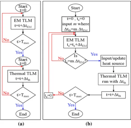
2009,2010; Boyer et al.2002; Chen et al.2012; Gobin et al.2007; Hu and Hartland2002; Plech et al.2004; Romanova et al.2009). The numerical modelling of these phenomena has been restricted to either modelling of a purely thermal process using a time-domain diffusion equation (Baffou et al. 2009, 2010), or using an electromagnetic-thermal approach whereby the steady state solution of the EM field is used as an input excitation to the thermal model (Baffou et al.2009,2010; Chen et al.2012). Although in these models the essence of the EM and thermal field evolution is captured, the EM and thermal domain models are essentially decoupled and the material parameters are assumed to be constant. This is schematically shown in Fig.1a, where cumulative power loss of the EM model is used to excite the thermal simulation and where EM and thermal simulations are performed separately, generally using different time steps (DtEM=Dtth) for the same real timeTmax. This is clearly inadequate if temporal sources are considered and in scenarios where the material parameters are frequency dependent as is the case of a metal at optical frequencies.
In this paper a coupled time-domain electromagnetic and thermal method based on Transmission Line Modelling (TLM) method is developed to reflect the multi-physics
[image:2.439.92.347.353.601.2]nature of the optically induced heating process. On their own, electromagnetic (EM) TLM and thermal TLM methods are well established methodologies for the modelling of electromagnetic wave propagation and thermal diffusion processes, respectively. The EM TLM method is an unconditionally stable time domain numerical method (Christopoulos
1995) that allows for great flexibility when modelling complex geometries and materials (Paul1998). The EM TLM method uses the analogy between the EM field propagation and the voltage impulses travelling through a network of inter-connected transmission lines. Transmission lines are represented using equivalent RLC circuit equivalents and voltage propagation through the structure is solved in a time-stepping process of alternating scatter and connect operations (Christopoulos 1995). The background material in EM TLM is assumed to be free space and different material properties such as conductivity, permit-tivity and permeability are incorporated using transmission line stubs (Christopoulos
1995). Dispersive and frequency dependent properties are implemented using digital filters methodology (Paul 1998). Traditionally TLM has been used for microwave applications but it has also proved useful at optical frequencies (Janyani et al.2004; Meng et al.2013; Phang et al. 2013) The electromagnetic properties of plasma and a range of plasmonic devices such as a Surface Plasmon Polariton Waveguide Bragg Grating (SPP-WBG) and a dielectric surface grating for beam focusing applications have also been modelled in the TLM using the digital filter approach (Ahmed et al.2010; Paul et al.1999).
The thermal TLM uses the analogy between the heat equation and the EM wave equation to simulate the conductive heat diffusion through a network of lossy transmission lines whereby thermal properties such as the thermal conductivity and heat capacity of materials are mapped onto the equivalent resistances and impedances in the transmission line model (De Cogan 1998). The background material in the thermal model is chosen to be the material with the lowest time RC constant among the materials used in the model. Different materials are modelled using the link-stub technique (De Cogan1998; Patel1994). The thermal TLM model has previously been used for heat flux modelling in several applications such as semiconductor devices (Hocine et al.2003), microwave heating process (Flockhart
1994) and modelling of magneto-optic multi-layered media (Williams et al.1996). The multi-physics nature of optical heating is in this paper described as follows: The electromagnetic TLM model is used to model electromagnetic scattering of the optical wave in the plasmonic waveguide. The metal at optical frequencies cannot be assumed to be a perfect conductor and is highly lossy, dispersive and frequency dependent. As such the metal is described using the Drude model (Ramo et al. 1997) and the Z-transform that facilitates the translation between frequency responses of the filter to the time domain of the numerical method. The losses in the metal will give rise to the heating which is used as a heat source in solving the temporal heat diffusion using the thermal TLM. The coupling process is presented in Fig.1b where coupling is done from the EM to thermal models at specified time intervalsDtthand where both EM and thermal simulations are run in parallel. The temporal time step of the EM simulation is fixed but the time step of the thermal simulation can in practice be much larger than that of the EM simulation; in the present model it can bemtimes larger wheremis a positive integer.
interface. The strong confinement of the EM field at the waveguide tip will result in high ohmic losses and heating of the Au around the waveguide tip.
The paper is organized as follows: in the next section the plasma model and a brief description of the EM and thermal model are given followed by a description of the coupled EM-thermal algorithm. This is followed by the results on temperature distribution, thermal field convergence and temperature rise for a variety of input mesh sizes and power excitations to demonstrate the convergence and self-consistency of the model. The results are also compared to those calculated and obtained experimentally by (Desiatov et al.
2014). In (Desiatov et al. 2014) the optical simulations were performed using Finite-Difference Time Domain (FDTD) and Finite Element Method (FEM) analyses and the thermal simulations by a FEM approach. Finally some conclusions are given in Sect.4.
2 The model
2.1 The electromagnetic (EM) model
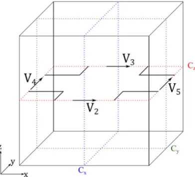
In order to simulate the propagation of the fundamental TM optical mode, the series TLM node shown in Fig.3 is used. This node configuration allows for a magnetic field
Fig. 3 The 2D TLM series node
[image:4.439.193.393.57.181.2] [image:4.439.196.392.435.612.2]component along the longitudinal direction Hz and transversal electric fields Ex andEy (Christopoulos,1995). The node is of the sizeDx=Dy=DlwhereDxis typically\k/10 wherekis the wavelength at the highest frequency of interest. The node has four ports at which it is connected to neighbouring nodes and at which the electric fields are related to voltage impulsesV2,V3,V4,V5.
At each port the incident and reflected voltage impulses at each node can be defined usingViandVrmatrices respectively in the form of
Vi¼ Vi
2V3iV4iV5i
T
;
Vr¼ Vr
2V r 3V r 4V r 5 T
; ð1Þ
where superscript ‘‘T’’ denotes transpose of the matrix.
The nodal excitation fields matrixFiis related to incident voltages as (Paul1998)
Fi¼ Vi
x Vyiiiz
h iT ; Vi x Vi y ii z 2 4 3 5¼
1 1 0 0
0 0 1 1
1 1 1 1 2 4 3 5 Vi 2 Vi 3 Vi 4 Vi 5 2 6 6 4 3 7 7 5¼RiVi;
ð2Þ
where Ri is the cell excitation matrix. The nodal voltage and nodal current are then obtained from the excitation field matrix using
F¼ VxVyiz
T ; Vx Vy iz 2 6 4 3 7 5¼
tex 0 0 0 tey 0 0 0 tmz 2 6 4 3 7 5 Vi x Vi y ii z 2 6 4 3 7
5¼TFi; ð3Þ
whereTis the transmission coefficient matrix andtex,teyandtezdepend on the normalized parameters of the modelled material. For a material with constant electric and magnetic parameters the general transmission coefficients for the series 2D-TLM node are obtained from (Paul1998),
tex¼tey¼ 2 2þgeþsve
;
tmz¼ 2 4þrmþ2svm
;
ð4Þ
whereve,vm,ge,rmandsare the electric susceptibility, magnetic susceptibility, normalized electric conductivity, normalized magnetic resistivity and normalized Laplace variable, respectively.
The nodal voltage and current obtained from Eq.3 are then transformed into the Z-domain using the bilinear transform:
s¼ s
Dt¼
2 Dt
1z1
1þz1 ð5Þ
Frequency dependent materials are modelled in the same fashion by replacing the electric or magnetic parameters such as susceptibility or conductivity with their corre-sponding frequency dependent parameters.
In this paper the metal is described using a frequency dependant parameters using the Drude model (Luebbers et al.1991):
e xð Þ ¼e0 1þ x2
p xðjmcxÞ
!
¼ereð Þ x jeimð Þ;x ð6Þ
wherexpis the plasma frequency in rad/s,mcis the plasma collision frequency,e0is the permittivity of free space,xis the angular frequency, andeim(x) andere(x) are the imaginary and real components of the plasma permittivity respectively. Complex dielectric constant is implemented in the TLM method using the Z-transform and digital filter method (Paul1998) and will not be covered in detail here. The imaginary part of the complex dielectric index represents the material conductivity component that is responsible for the power dissipation in the metal. The heat source of the thermal model is obtained from the instantaneous power losses in the EM model as a consequence of the material conductivity. At optical frequencies the conductivity of a plasmonic material can be approximated to be (Ordal et al.1985),
re¼
x2 p 4pmc
; ð7Þ
wherereis electrical conductivity in S/m.
The instantaneous power loss at every TLM node can be obtained using the general formula for dissipated power density (Orfanidis et al.2014)
Pd½ ¼n 1 2rejE n½ j
2
; ð8Þ
wherenrepresents the node,Pdis the power dissipated per unit volume at the node in W/ m3andj jE is the electric field in V/m at each node, obtained asj j ¼E ffiffiffiffiffiffiffiffiffiffiffiffiffiffiffiffiE2
xþE2y q
.
2.2 The thermal model
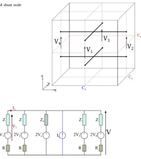
The thermal TLM utilizes the shunt node configuration of the TLM model (Christopoulos
1995) as shown in Fig.4.
The Thevenin equivalent circuit for the 2D-thermal model (De Cogan1998) has to be modified to accommodate a current source that will act as a heat source at the node. The thermal node has to implement the stub technique (Christopoulos1995) in order to model different materials in real applications. The TLM circuit parameters are related to the material thermal properties through (Newton1994)
Z¼Dt
C ¼
2Dt
qCpADl
;
R¼ Dl
2KthA
;
Zs¼ Dt
2 1
Cs
;
ð9Þ
nodal length,Kthis the thermal conductivity andCsis the stub capacitance evaluated from (Newton1994)
Cs¼CmCb; ð10Þ whereCmis the material thermal capacitance andCbis the background material thermal capacitance.
Figure5shows the Thevenin equivalent circuit for the thermal node used in this paper, whereVis the nodal voltage,Ris the node thermal resistance,Isis the nodal heat source,
Vi
1; V2i; V3iandV4i
are the node ports’ incident voltages.
The value of the current source at each node is obtained at coupling intervals using Eq.8, where the mapping from power to current is given by
Is¼Pd½ n Dl A; ð11Þ where A is the nodal area. The nodal voltage at the node is then calculated using
V¼2
Vi
1 ZþRþ
Vi
2 ZþRþ
Vi
3 ZþRþ
Vi
4 ZþRþ
Vi s
Zs
þIs 4
ZþRþ 1 Zs
ð12Þ
Fig. 5 The Thevenin equivalent for the 2D thermal node
[image:7.439.112.392.53.369.2] [image:7.439.193.394.56.236.2]The voltage here is representing the temperature (T); the presentation is a voltage to maintain consistency with the circuit theory analogy.
The TLM scatter and connect processes for thermal problems are described in De Cogan (1998).
The thermal parameters of the materials used in the model are those of an ambient temperature of 25C. The outer boundary conditions for the thermal model are modelled as a heat sink at ambient temperature.
The principal difficulty in coupling the EM and thermal TLM models lies in the fact that the simulation time steps of the EM and thermal models are different. The simulation time step of the thermal model defines its stability and needs to satisfy (De Cogan and De Cogan
1997),
DtthRthCth; ð13Þ
where Rthand Cthare the lowest product of thermal resistance and the thermal capacitance in the thermal model.
Typically, the time step of the thermal model that satisfies Eq.13is many orders of magnitude higher than the time step of the EM model, which means that that the overall timescales of EM and thermal models are different. The choice of thermal time step is thus important for stable coupling between the EM and thermal models. Generally setting the thermal time step to be equal to the electrical time step will guarantee the stability of the thermal model due to the fact that thermal diffusion is much slower than the interaction of the EM waves. However, this choice would increase the computational resources of the model. It would be desirable to increase the thermal time step and coupling intervals so that both the accuracy and the stability of the method are ensured and both EM and thermal simulations are effectively running in parallel over the same time frame as shown in Fig.1b. In the following section the choice of the thermal time step is discussed in terms of the accuracy and stability of the coupled method.
3 Results
In this section the coupled EM-thermal model is used to simulate the EM field propagation and conduction heat diffusion for the 2D nanotip waveguide structure shown in Fig.2. The silicon slab waveguide has a width of 1lm and a length of 3lm. The triangular tapered area has a base of 0.45lm and a length of 1lm with the nanotip of 20 nm diameter to focus the light at the end of the waveguide. The silicon waveguide core has an effective refractive index of 3.3917 at the operating frequency of 1.55lm and the air as the cladding material. The material parameters for gold are xp=1.3673491016rad/s and mc=6.4691013Hz (Ordal et al. 1985). The silicon is considered to be lossless in this model as silicon conductivity is negligible at the operating frequency. All EM material parameters are kept constant in the model.
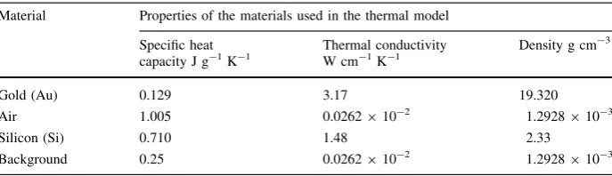
The material properties for the gold, air and silicon used in the thermal model are the specific heat capacity, density and thermal resistance at the ambient temperature of 25C; these are summarised in Table1(Benenson et al.2002; Min et al.2011). The background material is an artificial material with a lower diffusion constant than all the other materials used in the model to satisfy the stability condition in Eq.13.
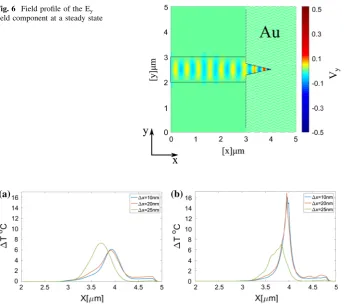
DtEM=2.3586910-17and the total simulation time is 63.6 ps. Figure6shows that the maximum of the field is at the nano-tip, which will effectively result in large Joule heating in this area.
In order to investigate the convergence of the coupled-method results with the mesh size Fig.7a, b shows the temperature distribution along the middle of the plasmonic waveg-uide, i.e., in the y=2.5lm plane, for different mesh sizes, namelyDx=25,Dx=20 and Dx=10 nm. The time steps of the EM and thermal models are kept the same as DtEM=Dtth=2.3586910-17s. Two different cases are considered, namely (a) an uncoupled EM-thermal where a complete EM simulation is done until the field reaches steady state and the power losses at the end of simulation are used as an input to the thermal model, and (b), where the power losses of the EM model are used as an input to the thermal at every time step. The input optical source power in both cases is taken to be 10 mW.
Figure7a shows that as the mesh size is reduced the temperature distribution converges but the temperature distribution is spread across the waveguide tip. Similarly, in the case of coupling at every time step, Fig.7b shows that as the mesh size is reduced the thermal distribution converges. Comparing with Fig.7a it can be seen that the thermal profile of Fig.7b results in a thermal distribution that is much more focused at the tip of the waveguide, i.e., atx%4lm.
Additionally, the maximum temperature achieved at the waveguide tip is much higher in the case of EM-thermal coupling. In both cases the coarse mesh with the discretisation Dx=25 nm doesn’t represent the nano-tip thermal profile accurately, resulting in the maximum temperature just before rather than at the tip of the taper itself; this is a con-sequence of the stair-casing error that is common when discretising planes that do not align with Cartesian coordinates. As the mesh size is reduced the taper profile is modelled more accurately resulting in the maximum field at the tip of the taper, as expected. Figure7b confirms that the convergence is reached for a mesh size of 20 nm or smaller.
[image:9.439.48.392.70.169.2]To further investigate the thermal profile, Fig.8a, b plots the thermal field distribution after 82.78 ps of the simulation time for the uncoupled and coupled EM-thermal models usingDx=20 nm and an input optical power of 10 mW. The uncoupled model results show a wider spatial spread but lower maximum temperature (*8C) due to the fact that all the thermal energy is given once at the beginning of the modelling process as shown in Fig.8a. Figure8b shows that thermal profile of the coupled EM-thermal model results in a more focused profile with higher maximum temperature compared to Fig.8b. In the case of the coupled model the regular application of the input thermal source resulting from the EM simulation leads to higher temperatures and temperature distribution more focused at places where the EM field is strongest as shown in Fig.7. The result of Fig.7b compares
Table 1 Material properties used in the thermal model
Material Properties of the materials used in the thermal model
Specific heat
capacity J g-1K-1 Thermal conductivityW cm-1K-1 Density g cm -3
Gold (Au) 0.129 3.17 19.320
Air 1.005 0.0262910-2 1.2928910-3
Silicon (Si) 0.710 1.48 2.33
very well with the simulations and measurements of (Desiatov et al. 2014) where the maximum temperature rise is*15C. The small differences might occur due to the fact that a 2D model is considered in this paper.
Results reported in Figs.7and8b assume coupling from the EM model to thermal at every time step and that both thermal and EM time steps are equal. For a mesh size of Dx=20 nm the the EM time step is DtEM=4.717910-17s and the maximum stable time step for the thermal model istth &1.57910-13s. Running the simulation at the EM time step is clearly not computationally efficient. However, the significant dif-ference in the time steps allows for the thermal time step to be as small as EM time step and up to a maximum of Dtth(max) determined by Eq. (13) in order to maintain the stability of the thermal model. It is clearly more efficient to run the thermal model at time stepsDtth[DtEMwhilst still ensuring that the coupling from the EM to thermal is done at every Dtth. Figure9 plots the maximum temperature rise in the model using different thermal time steps such that they are integer multiples of the EM time step DtEM. The results are shown forDtth/DtEM =1, 625, 1350 and 2500 and are also compared with the uncoupled approach of Fig.1a. The results of Fig.9 show that for a ratio of Dtth/ DtEM\625 there is no big difference compared to the case when both thermal and EM
Fig. 6 Field profile of the Ey
field component at a steady state
[image:10.439.51.396.54.360.2]time steps are the same (Dtth/DtEM=1). The uncoupled method results in an underesti-mation of the overall temperature rise.
The maximum temperature rise within the same time frame will depend on the input power intensity of the optical source. The relationship between the optical source power
Fig. 8 The thermal profile for
athe uncoupled model and
bcoupled model
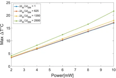
[image:11.439.96.395.47.539.2] [image:11.439.221.396.53.360.2]and the maximum temperature at the same overall simulation time of 82.76 ps is plotted in Fig.10for the mesh sizeDx=20 nm. The results are plotted for different thermal time steps namelyDtth/DtEM=1, 625, 1350 and 2500 and the EM to thermal coupling is done every thermal time step. Figure10shows that in all cases the maximum temperature is linearly dependent on the input optical power which compares well with the experimental results of (Desiatov et al.2014).
4 Conclusion
A stable electromagnetic (EM)-thermal multi-physics coupled model of EM-induced heating in a plasmonic tapered waveguide is demonstrated. The model calculates the accumulative power loss in the EM model and uses it as a source for the thermal model at regular time intervals. The results show that regular coupling from the EM to thermal method is an important factor to consider and that this will affect the accuracy of the overall coupling method. The results show that the computational efficiency of the coupled method can be improved if the thermal time step is up to two orders of magnitude greater than the EM time step whilst ensuring that the EM to thermal coupling is done at every thermal time step. The simulated results compare very well with the experimental results of (Desiatov et al.2014). The linear relation between the optical source power and the maximum temperature rise is also verified and compares well with the experimental results.
Open Access This article is distributed under the terms of the Creative Commons Attribution 4.0 Inter-national License (http://creativecommons.org/licenses/by/4.0/), which permits unrestricted use, distribution, and reproduction in any medium, provided you give appropriate credit to the original author(s) and the source, provide a link to the Creative Commons license, and indicate if changes were made.
References
[image:12.439.109.334.56.207.2]Ahmed, O.S., Swillam, M.A., Bakr, M.H., Li, X.: Modeling and design of nano-plasmonic structures using transmission line modeling. Opt. Express18(21), 21784–21797 (2010)
Atwater, H.A., Polman, A.: Plasmonics for improved photovoltaic devices. Nat. Mater.9, 205–213 (2010) Baffou, G., Quidant, R., Garcı´a de Abajo, F.J.: Nanoscale control of optical heating in complex plasmonic
systems. ACS Nano4, 709–716 (2010)
Baffou, G., Quidant, R., Girard, C.: Heat generation in plasmonic nanostructures: influence of morphology. Appl. Phys. Lett.94, 153109 (2009)
Benenson, W., Harris, J.W., Stocker, H., Lutz, H. (eds.): Handbook of Physics. Springer, New York (2002) Boyer, D., Tamarat, P., Maali, A., Lounis, B., Orrit, M.: Photothermal imaging of nanometer-sized metal
particles among scatterers. Science297, 1160–1163 (2002)
Chen, X., Chen, Y., Yan, M., Qiu, M.: Nanosecond photothermal effects in plasmonic nanostructures. ACS Nano6, 2550–2557 (2012)
Christopoulos, C.: The Transmission-Line Modeling Method TLM. IEEE Press, New York (1995) De Cogan, D., De Cogan, A.: Applied Numerical Modelling for Engineers. Oxford Univeristy Press, Oxford
(1997)
De Cogan, D.: Transmission Line Matrix (TLM) techniques for diffusion applications. Gordon and Breach Science Publishers, Amesterdam (1998)
Desiatov, B., Goykhman, I., Levy, U.: Direct temperature mapping of nanoscale plasmonic devices. Nano Lett.14, 648–652 (2014)
Fang, Z., Zhen, Y.R., Neumann, O., Polman, A., Garcı´a De Abajo, F.J., Nordlander, P., Halas, N.J.: Evolution of light-induced vapor generation at a liquid-immersed metallic nanoparticle. Nano Lett.13, 1736–1742 (2013)
Flockhart, C.: The simulation of coupled electromagnetic and thermal problems in microwave heating. In: Second International Conference on Computation in Electromagnetics. pp. 267–270. IEE, London (1994)
Gobin, A.M., Lee, M.H., Halas, N.J., James, W.D., Drezek, R.A., West, J.L.: Near-infrared resonant nanoshells for combined optical imaging and photothermal cancer therapy. Nano Lett.7, 1929–1934 (2007)
Hocine, R., Boudghene Stambouli, A., Saidane, A.: A three-dimensional TLM simulation method for thermal effect in high power insulated gate bipolar transistors. Microelectron. Eng.65, 293–306 (2003) Hu, M., Hartland, G.V.: Heat dissipation for Au particles in aqueous solution: relaxation time versus size.
J. Phys. Chem. B106, 7029–7033 (2002)
Janyani, V., Paul, J.D., Vukovic, A., Benson, T.M., Sewell, P.: TLM modelling of nonlinear optical effects in fibre Bragg gratings. IEE Proc.: Optoelectron.151, 185–192 (2004)
Liu, G.L., Kim, J., Lu, Y., Lee, L.P.: Optofluidic control using photothermal nanoparticles. Nat. Mater.5, 27–32 (2006)
Luebbers, R.J., Hunsberger, F., Kunz, K.S.: A frequency-dependent finite-difference time-domain formu-lation for transient propagation in plasma. IEEE Trans. Antennas Propag.39, 29–34 (1991) Meng, X., Sewell, P., Vukovic, A., Dantanarayana, H.G., Benson, T.M.: Efficient broadband simulations for
thin optical structures. Opt. Quantum Electron.45, 343–348 (2013)
Min, R., Ji, R., Yang, L.: Thermal analysis for fast thermal-response Si waveguide wrapped by SiN. Front. Optoelectron.5, 73–77 (2011)
Newton, H.R.: TLM models of deformation and their application to vitreous china ware during firing.
https://hydra.hull.ac.uk/resources/hull:3499(1994)
Ordal, M.A., Bell, R.J., Alexander, R.W., Long, L.L., Querry, M.R.: Optical properties of fourteen metals in the infrared and far infrared: Al Co, Cu, Au, Fe, Pb, Mo, Ni, Pd, Pt, Ag, Ti, V, and W. Appl. Opt.24, 4493–4499 (1985)
Orfanidis, S.J.: Electromagnetic Waves and Antennas.http://www.ece.rutgers.edu/*orfanidi/ewa/(2014) Patel, H.C.: Non-linear 3D modelling heat of flow in magneto-optic multilayered media, Ph.D. thesis,
University of Keele (1994)
Paul, J.: Modelling of general electromagentic material properties in TLM, Ph.D. thesis, University of Nottingham (1998)
Paul, J., Christopoulos, C., Thomas, D.W.P.: Generalized material models in TLM Part I: materials with frequency-dependent properties. IEEE Trans. Antennas Propag.47, 1528–1534 (1999)
Phang, S., Vukovic, A., Susanto, H., Benson, T.M., Sewell, P.: Ultrafast optical switching using parity–time symmetric Bragg gratings. J. Opt. Soc. Am. B30, 2984–2991 (2013)
Plech, A., Kotaidis, V., Gre´sillon, S., Dahmen, C., Von Plessen, G.: Laser-induced heating and melting of gold nanoparticles studied by time-resolved X-ray scattering. Phys. Rev. B Condens. Matter Mater. Phys.70, 1–7 (2004)
Romanova, E.A., Konyukhov, A.I., Furniss, D., Seddon, A.B., Benson, T.M.: Femtosecond laser processing as an advantageous 3-D technology for the fabrication of highly nonlinear chip-scale photonic devices. J. Lightwave Technol.27, 3275–3282 (2009)
Wang, L., Li, B.: Thermal memory: a storage of phononic information. Phys. Rev. Lett.101, 1–4 (2008) Wassel, H.M.G., Dai, D., Tiwari, M., Valamehr, J.K., Theogarajan, L., Dionne, J., Chong, F.T., Sherwood,
T.: Opportunities and challenges of using plasmonic components in nanophotonic architectures. IEEE J. Emerg. Sel. Top. Circuits Syst.2, 154–168 (2012)