TPEL-Reg-2014-10-1702.R1
Abstract— The need for multidisciplinary virtual prototyping in power electronics has been well established however design tools capable of facilitating a rapid, iterative virtual design process do not exist. A key challenge in developing such tools is identifying and developing modelling techniques which can account for 3D, geometrical design choices without unduly affecting simulation speed. This challenge has been addressed in this work using model order reduction techniques and a prototype power electronic design tool incorporating these techniques is presented. A relevant electro-thermal power module design example is then used to demonstrate the performance of the software and model order reduction techniques. Five design iterations can be evaluated, using 3D inductive and thermal models, under typical operating and start-up conditions on a desktop PC in less than 15 minutes. The results are validated experimentally for both thermal and electrical domains.
Index Terms—Modeling, Power electronics, Computer aided analysis, Design automation, Electromagnetic analysis, Finite difference analysis, Power converter, Time domain analysis.
I. INTRODUCTION
A. Requirements for Virtual Prototyping and Virtual Design Optimization1
irtual prototyping is the concept of using software to evaluate the performance of prospective power electronic system, sub-system or component designs, thus eliminating the need for construction and testing of physical prototypes. Virtual prototyping therefore has the potential to reduce the time and cost involved in evaluating the performance of proposed design. Design optimization is an iterative process where many design iterations are used to evolve an initial design idea to the stage where it satisfies a set of design constraints and most closely matches a target design performance objective. Clearly, design optimization involves the evaluation of many prototypes and so virtual prototyping has the potential to increase the performance of power
This work was supported in parts by the Engineering and Physical Sciences Research Council, through grant EP/I013636/1and the EU FP7 program through the CleanSky JTI.
The authors are all with the PEMC Research Group, Faculty of Engineering, University of Nottingham, UK. (email:
paul.evans@nottingham.ac.uk, alberto.castellazzi@nottingham.ac.uk,
mark.johnson@nottingham.ac.uk)
electronic designs by allowing increased levels of design optimization within a fixed time-frame or budget. Ideally this optimization process will be automated or semi-automated to allow efficient exploration of the design space.
Rapid multi-domain physical simulation is the key enabling technology for virtual prototyping and virtual design optimization; simulations are needed to predict the effect that design choices – the choice of components, materials and geometrical design – have on overall system performance. Typical physical domains that are of interest in power electronic systems include electrical parasitics[1, 2], EMI[3, 4], electric field in high voltage designs[1], thermal[5] and mechanical[6, 7]. The speed of these multi-domain simulations is important as it will determine the speed and ease of use of the virtual prototyping process. Use of virtual prototyping in design optimization compounds the problem: as many design iterations require many simulations, with changes to the design geometry made at each iteration. The physical models must be therefore be updated and so an efficient, automated process for generating these models from generally applicable, fundamental physics must be available. It must also be possible to couple the physical models with non-physical models of linked components: for example behavioral models of loads such as machines, supply models, control electronics and semiconductor switches.
Once the multi-domain simulation can be performed efficiently, the requirements then shift to the design of the virtual prototyping tools, for example: the required multi-disciplinary model description methods, the integration of design optimization techniques and overall non-expert user-friendliness of the design tool, as is identified in [8].
B. Existing Solutions
Existing commercial physical simulation tools are usually designed for detailed simulation in one domain and are optimized for generality and completeness, rather than computational efficiency and multi-domain optimization. Some previous work has combined these individual tools to form a multi-disciplinary simulation platform [9-11] and while it is possible to achieve multi-domain simulation of almost any design, the speed of these simulations and user-friendliness of the design process are poor. This approach may be a good choice for certain detailed investigations (e.g.[11]) but is not well suited to a general use power electronics design and optimization tool. The model speed limitation may be overcome by using simplified analytical expressions to
Design Tools for Rapid, Multi-Domain Virtual
Prototyping of Power Electronic Systems
Paul L. Evans, Alberto Castellazzi, and C. Mark Johnson,
Member, IEEE
TPEL-Reg-2014-10-1702.R1
Fig. 1 – Chopper cell circuit and 3D model of semiconductor packaging component. Layers not to scale. describe system behavior as function of geometry[12] but
these expressions must be developed individually by the designer for specific cases (e.g. specific topologies or range of operating conditions). The challenge for virtual prototyping is to combine the generality of physical modelling tools with the speed of analytical models in a user-friendly integrated design environment.
An approach often used for multi-domain physical simulation in power electronics is the compact, lumped element, or equivalent circuit model. This approach discards spatial information (and sometimes accepts reduced accuracy) in order that the key system properties can be expressed using relatively few, simple ordinary differential equations which are commonly represented as an equivalent circuit. Quasi-static electromagnetic parasitic[2] and thermal [13] effects are often reduced to these equivalent electrical circuits, but potentially this could also be applied to magnetic and mechanical design problems. This process is often used since it allows physical models in different domains to be combined in a common simulation platform with behavioral models of other system components. Commercial software vendors also offer this approach since it allows them to make use of their existing tools for domain specific model extraction, for example the Ansys Simplorer system simulator can import extracted models from the Ansys suite of simulation packages. The difficulties with this approach for virtual design optimization are that: 1) a process must exist to generate these equivalent circuits from a 3D model of the design, which for virtual design optimization must be automated and computationally efficient, and 2) the models must then be automatically exported from the modelling software and assembled in the circuit simulator. An overall control mechanism is therefore required to automate the data flow from 3D design description and modification, to model extraction, to circuit simulator import and interconnection. The general trend in power electronics virtual prototyping now appears to be automating this fundamentally manual approach. Existing research has tackled the model generation challenge, for example thermal compact model generation[14], quasi-static electromagnetic model generation[15] and the implementation of these models into circuit simulators[16]. With the model generation addressed, the weaknesses is then the integration or coupling of the various modelling tools and circuit simulator, as is identified in [17] which outlines a vision for more integrated power electronics design tools. A solution is presented in [17] which has been implemented in new virtual prototyping tools by Gecko Research[18],
however in the published results from this software, the “circuit simulator + imported equivalent circuit model” philosophy persists. Some additional ideas about the use of Model Order Reduction techniques for the generation of these circuit models is presented in [20], (thesis only available in German).
These newer Model Order Reduction (MOR) techniques such as the Krylov subspace projection algorithms can also allow direct acceleration of 3D thermal and electromagnetic simulations, eliminating the need to generate equivalent circuit models. Some of these are beginning to be implemented in commercial software such as the techniques developed in MOR for Ansys[19], which are now present in the more recent Ansys releases where they can be used for accelerating thermal simulations. This work will show that by applying these techniques to both the thermal and parasitic modelling challenges, and integrating the techniques into a single design and simulation tool, the model extraction and import methodology can be eliminated and more tightly integrated power electronic design software with an improved user experience can be developed.
C. Proposed Design Tool
The aims of this work are to demonstrate how a single, power electronics specific design tool can be developed to allow fast multi-domain simulation and virtual design optimization. A prototype design tool has been developed and a design example will be used to demonstrate its operation. The development goals for the tool were:
Integrated 3D model representation – the ability to represent and view the system in 3D within the tool.
Accelerated physical modelling capabilities with no equivalent circuit model extraction.
Automated design optimisation capabilities for virtual design optimisation.
Full featured, 3D post-processing (e.g. temperature, current distribution plots) without slow FEA type simulations.
TPEL-Reg-2014-10-1702.R1
commutation loop which will increase the MOSFET turn-off voltage overshoot, but with increased dx comes increased device spacing and therefore lower device temperatures.
[image:3.595.63.250.263.376.2]The design tool allows both parts of this system to be described: firstly the power module and heat-sink assembly, whose design is of interest, is described as a geometrical 3D model. The remainder of the system including the semiconductor models is described as an equivalent circuit or behavioral model. Numerical methods and Model Order Reduction techniques are used to generate efficient 3D models describing the part of the system described geometrically, in this work both thermal and inductive parasitic behavior are considered, The complete system is then simulated in the time domain, The design tool structure is described in Fig. 2.
Fig. 2 – Design Tool Structure
II. DESIGNTOOLIMPLEMENTATION A. Model Representation
The developed tool allows a design to be input as a 3D model, so the effect of design choices on performance can be evaluated. Attempting to model all components physically can result in over-complicated models with problems including poor convergence and long execution times. Components such as semiconductor devices may be practically impossible to model using physical models within a wider system simulation. The solution to this is to enable some components to be modelled with behavioral models as is common in many existing power electronics simulation packages. This results in a split simulation where a set of behavioral models, which can have properties in electrical, thermal or other domains, execute in parallel with a multi-disciplinary 3D model of the remainder of the system. Components can be modelled behaviorally if their physical properties and therefore behavior will be unaffected during the design process, and if interaction of the component with other components can be restricted to occurring at a small number of well-defined terminals or boundaries. Conversely, components whose design may change during the design process or where significant distributed interaction with other components exists (e.g. magnetic field coupling between two inductors) must be represented in a unified physical model. The single physical model for each domain ensures effects such as the
inter-component electromagnetic coupling are accounted for. This allows flexible representation where the part of the system whose design is being optimized (the semiconductor packaging in this design exercise but this could also be integrated magnetic components, for example) to be represented and simulated physically and the remainder of the system represented with behavioral models of appropriate fidelity.
The 3D design geometry is defined in terms of building blocks such as 3D solids, and electrical and thermal boundaries. These basic building blocks can be grouped to form components such as power modules, substrate tiles, heat-sinks or bus-bars, which are then in turn grouped to form the final design for a system or sub-system such as the power module and heat-sink shown in Fig. 1. Components or sub-system geometrical or behavioral models can be stored in library files for re-use new designs. The boundaries serve as points to which the behavioral models of the remainder of the system can be connected for design evaluation. The solids and boundaries can be defined from primitives such as cuboids and features are available to allow the easy implementation of power electronics specific entities such as wire-bonds. A simple design such as the example in this work could be entered in under 10 minutes.
Behavioral models are defined using SPICE syntax and are constructed from elementary passive circuit branches (R,L,C), current and voltage source branches and switch branches. Different source models (DC, Pulsed, PWM, Sinusoidal) and semi-ideal electro-thermal switch and diode models are currently available. If these models are connected to thermal boundaries instead of electrical, the current and voltage variables are treated as heat-flux and temperature allowing behavioral thermal models to also be implemented, similar equivalencies could be made for other domains such as mechanical (velocity, force), magnetic (flux, mmf) in the future. The hierarchical component grouping structure acts as an addressing system allowing connection of the behavioral models to the geometry boundaries (Fig. 3). The text based SPICE description would be replaced with a graphical circuit diagram in future work.
Fig. 3 – Example SPICE Load Model Input
TPEL-Reg-2014-10-1702.R1
Fig. 6 – Generalised Physical Model Generation Procedure B. Design Process Control
The design process is controlled by a scripting interface which allows parameter sweeps and other design functions to be used. The custom scripting language builds on the capabilities of the component parameter sweeps (e.g. resistor values) that are possible in software such as PSPICE by also allowing physical parameter sweeps: for example changing the location or dimension of component in the design. An example of this, used for the design example in this work, is shown in Fig. 4. The hierarchical geometry description is used to facilitate design manipulation. The scripting language can also be used to process simulation data, e.g. evaluate maximum/minimum values of waveforms produced to determine design direction and work is also underway to implement reliability or mechanical damage estimation post-processing capabilities. Additional work has also investigated allowing optimization algorithms to control the design variables, rather than using loops [20].
Fig. 4 – Example Design Process Control Script
C. Physical Modelling
A key requirement for virtual prototyping is the ability to efficiently account for the effect of geometrical design choices on system performance, which requires carefully chosen simulation techniques. An approach based on spatial discretization (meshing) of the geometry and model order reduction is proposed here and demonstrated for thermal and inductive parasitic effects. The physical model is coupled to the behavioral components at the small number of defined boundaries at which variables common to both the physical model and the behavioral representation exist, for example total heat generation across a defined volume or the voltage at a defined point.
The design tool can generate both thermal and electrical parasitic physical models; the coupled variables at thermal boundaries are heat-flux and temperature, and at electrical boundaries current and voltage. A numerical method is then used to generate a system of equations which describe the relationship between these boundary variables based on the physical description of the design geometry. In this work
electrical boundaries are defined as a node, the voltage at this node becomes the input to the 3D electrical model, the current flowing into this node from the coupled behavioral model is the output. For the thermal model, a surface or volume region is defined over which the input variable, heat flux, flows into the model. The temperature at a point in the centre of this region becomes the model output variable. A common problem with discretization based numerical methods is that in order to generate equations from an arbitrary physical description, the discretization approach results in a very large number of equations,n, (typically of order 103-106) depending
on method and geometry. The large number of equations is due to the large number of nodes required to accurately capture the detail in the physical geometry.
The proposed solution to this problem is MOR. The principle behind MOR techniques is that although the n equations give rise to n eigenvalues spread over the model’s frequency response range, the solution can in fact be accurately represented using a much smaller set of distinct eigenvalues. The projection based MOR techniques used in this work consider the original model with n equations as being defined by n eigenvalues and eigenvectors in n -dimensional space. The techniques assume it is possible to define anm-dimensional subspace, wherem<<n, onto which the model can be projected. This subspace must be defined so that the projection will capture the dominant properties of the original model. Providing the subspace has been chosen correctly, the projected model defined by a new set of m eigenvalues and eigenvectors in the m-dimensional subspace, will accurately capture the dominant dynamics of the original model but with far fewer equations. The algorithms used in this work use the mth-Krylov subspace for projection and more information on these algorithms can be found in [21-23]. The projection process generates a linear transform between
[image:4.595.72.511.672.733.2]TPEL-Reg-2014-10-1702.R1
the original and reduced order models. The algorithms produce an mxn matrix with orthonormal rows, H, which along with is transpose can be used to translate between the state vectors of the original and reduced order systems (1).
࢞࢘= [ܪ]࢞ (ܽ) ࢞= [ܪ]்࢞࢘ (ܾ) (1)
Related to this, a new set of mequations linking the inputs and outputs of the original system with the states of the reduced order system can be obtained (2-3).
[ܪ]ܯ[ܪ]்࢞
࢘̇ = [ܪ]ܣ[ܪ]்࢞࢘+ [ܪ]ܤ࢛
࢟=ܥ[ܪ]்࢞
࢘ (2)
Or: [ܯ]࢞࢘̇ = [ܣ]࢞࢘+ [ܤ]࢛
࢟= [ܥ]࢞࢘ (3)
The new model equations Mr,Ar,Br, andCraremxm,mxm, mxa andbxmin size compared with the original matrices M, A,BandCwhich were arenxn,nxn,nxaandbxn, whereais the number of inputs and b the number of outputs, so by substituting the original model with the reduced order model onlym equations need to be solved at each time-step. While the input and out variables of the reduced order model still represent the same physical quantities of the original, it should be noted that the states of the reduced order model no longer have any physical meaning. No spatial information is lost however, as the voltage, current, temperature and heat-flux values at any node in the original model can be calculated as a linear combination of the reduced order states using the H matrix (equation 1b). Therefore full 3D spatial post-processing and graphical analysis, at any time-step, is still possible. The volume of data required to be stored and processed for long simulations is also significantly reduced. If the order reduction process is fast enough and is embedded in the design tool, the appearance to the user is that large 3D physical models are executing in parallel with the circuit model at a speed usually only possible with circuit-only simulations. Hence, the need to reduce physical models to compact models or equivalent circuits is eliminated.
It is important to ensure that sufficient iterations of the MOR algorithm are performed so that a reduced order model with a sufficient number of states to accurately approximate the original is obtained. In this work, the size of the reduced order models is specified manually however it may be possible in the future to automatically determine this[24].
This fundamental model generation process is applicable to any physical modelling domain where suitable numerical methods, automatic-meshing algorithms and automated Model Order Reduction techniques exist. The software implementation at present is limited to linear thermal and inductive parasitic modelling techniques and specific details for these cases are given in the following sections.
1) Thermal
For the thermal model, the model generation process is
implemented using the Finite-Difference Method (FDM) for equation generation (as described in [14]) and the Block
Arnoldi algorithm(see [23]) for model order reduction. Application of the FDM results in a multiple-input-multiple-output linear system of equations where the inputs and multiple-input-multiple-outputs represent the locations at which thermal power flows into and out of the model, to which MOR can be applied. A structured or mapped meshing approach is used to simplify the automated meshing process. Meshing constraints (maximum node-spacing or minimum number of edge divisions) can be specified in the geometry description to ensure solution accuracy. Any component in the design can be marked as non-thermally conductive and will then be omitted from the thermal meshing process. A typical mesh produced for the design example is shown in Figure 2, over 40,000 equations are generated which would usually need be solved at each time-step if no MOR was used.
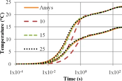
[image:5.595.315.512.124.262.2]Fig. 8 compares the temperature response at the center of the upper surface of the MOSFET and diode when 4.75W is applied to the MOSFET and 8.67W to the diode, from zero initial conditions, for 3 reduced order models and a reference waveform generated using Ansys FE software. The 25 term reduced order model is extremely accurate across the entire
Fig. 8 – Step response of reduced order models compared with Ansys generated reference.
[image:5.595.326.534.497.635.2]TPEL-Reg-2014-10-1702.R1
model response and even the 10 term model is accurate in steady-state and in the lower frequency range. The 25 term model represents a reduction in the number of equations by a factor of over 1,600.
The time taken to perform the order reduction for a range of reduced order and original model sizes is shown in Fig. 9. The model reduction time is predominantly determined by the number of nodes in the mesh as the most expensive operation during MOR is the factorization of the original model matrix into its L and U factors, this is performed once regardless of the size of the reduced order model and uses the KLU solver[25]. At present different mesh structures with similar numbers of nodes can have significant differences in factorization time which is thought to be because differences in the matrix structure affect the number of column and row ordering operations required during factorization. It is anticipated that improvements to the node numbering and equation generation procedure will rectify this issue. It should be possible to achieve a more consistent relationship between node number and extraction time close to the lower values seen in Fig. 9.
2) Inductive Parasitic
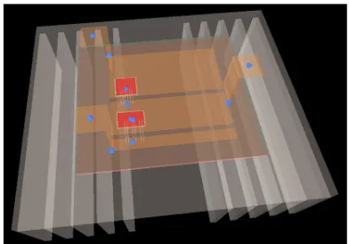
[image:6.595.314.511.89.228.2]The inductive PEEC method divides the conductive geometry into a mesh of equivalent conductors, a partial self-inductance and resistance for each inductor, and a mutual inductance between any two inductors, can be determined from an integral formulation of Maxwell’s equations[26]. A set of equations is then generated from this equivalent circuit of inductors and resistors using Modified Nodal Analysis (MNA). Nodes in this mesh can be defined as boundary points and referred to in the behavioral models, the voltage at, and current flowing into these points become the inputs and outputs to the parasitic model. Parasitic mesh constraints can be specified to control the mesh structure and the components to be included in the mesh specified in the geometrical description, the mesh is generated automatically from these rules for each design. A typical mesh structure is shown in Fig. 10, for this example the equivalent circuit had 943 circuit nodes interconnected by 1736 conductors which resulted in 2679 equations. Since this ‘circuit’ has only inductors and resistors in it, it is possible to use a mesh-analysis based equation generation process which would result in fewer
equations (only the conductor currents are solved for in mesh analysis). However, as MNA also solves for the node voltages it leaves the option for voltage plots to be easily constructed in the design tool and also allows for easy extension of the code to account for capacitive parasitics in future work. More information regarding this type of interconnect model can be found in [27, 28].
PRIMA[29] is used for MOR and it is a variation of the Block Arnoldi algorithm used for thermal modelling which is specifically designed to ensure stability and passivity of the reduced order model when the initial equations are derived using MNA. In this implementation, the number of terms in the reduced order model must be greater than or equal to the number of model inputs, 12, and the maximum number of iterations possible before convergence of the algorithm for this example is 21. The algorithm produces a new basis vector for the reduced order subspace at each iteration which must be normalized. As the algorithm converges the size of this basis vector approaches zero and the algorithm must be terminated, when the size approaches machine precision, complete convergence is assumed at this point. MOSFET switch-off VDS waveforms for reduced order models with 12 and 21
terms and a Fasthenry reference model, generated with the identical behavioral models, are shown in Fig. 11.
[image:6.595.63.254.94.206.2]There are relatively few distinct response modes in an inductive PEEC model, demonstrated by the fact that software such as Fasthenry or InCa3D can extract valid equivalent Fig. 9 – Time taken for thermal MOR for 5 and 20 term
reduced order models vs number of original equations, n, on
3.6GHz Core i7 Desktop PC Fig. 10 - Typical parasitic mesh generated for design example containing 1820 conductors and 986 nodes.
Fig. 11 – MOSFET turn-off Vdswaveform for reduced order
[image:6.595.315.526.585.708.2]TPEL-Reg-2014-10-1702.R1
inductance values for current loops at a single frequency. For this reason, fewer terms are required in the reduced order model compared with the thermal case where equivalent thermal impedances have a significant dependence on frequency over a wide bandwidth (e.g. Fig. 8).
The order reduction time (Fig. 12) is again strongly linked to original model size but the factorization is more expensive for a given matrix size due to the dense structure that arises from the mutually coupled inductors. With the PEEC method used for the electromagnetic model, the voltage and current variables in each mesh cell can potentially influence the voltage and current variables at all other cells which leads to a dense matrix structure with few non-zero elements. The nodal temperature variables in the FDM model are only directly related to adjacent nodal values, which leads to a sparse matrix structure with relatively few non-zero off-diagonal elements. It is much more difficult to solve the dense equations quickly, and with a solver not optimized for this type of problem the solve time can be have a dependence onn3, seen in Fig. 12.
This effectively limits the size of the original parasitic model to under 10,000 equations, More advanced techniques, such as the Fast Multipole Method[15, 30], a QR decomposition approach[31] or multiscale block decomposition approach in[32] , can overcome this limitation by using the geometry of the problem to avoid explicitly forming and solving these dense matrices and are a future option for accelerating the PEEC based MOR process, PEEC models including both inductive and capacitive elements could also be accelerated using this approach.
D. Multidisciplinary Time-Domain Simulation
The design tool takes the equations generated by the physical modelling procedures and combines them with the equations from the behavioral model. The design tool structure offers flexibility in the choice of modelling domains to be included, for example if no physical domains are included it becomes a power electronics circuit simulator, the parasitic model can be excluded for long-timescale thermal mission profile simulations driven by behavioral heat source models, or the thermal model can be omitted for detailed switching transient simulations or EMI simulations. This structure could also be extended to allow further physical domains, for example mechanical analysis, to be considered.
At each time-step, the behavioral switch and source models
can inform the solver when they would like the next time-step to occur. The solver keeps track of these requested steps in a queue (along with its default choice) and selects the next time-step based on the value at the front of the queue. This allows the fundamental time-step size to be quite large, but ensures that time-steps occur at all necessary points. Example uses are pulsed or PWM sources telling the solver when it needs the next time-step to occur so that its edges are defined properly, or a switch model requesting a certain number of closely spaced time-steps after it detects a state-change to capture transient switching behavior.
III. VALIDATIONEXAMPLEPARAMETERS A. Geometrical Parameters
Eleven test power modules were constructed: four with dx = 17, three with dx = 34.5 and four with dx = 52mm (Fig. 13). The MOSFETs were 650V Infineon CoolMOS 60R045CP die (11x7mm) and the diodes ABB 1200V, 100A die (8.4x8.4mm). These were soldered to the IMS substrate tiles using a Sn(96.4%)Ag(3.6%) solder, the source/anode connections using 6 375µm ultrasonically welded Aluminum wires. Two additional 125µm Aluminum wires were added to the MOSFET die at the gate, and source to allow for gate-drive connection and drain-source voltage measurements independent of the high current wires. Each module was painted matt black to allow accurate IR thermal imaging. The modules were mounted in turn to an aluminum heat-sink and connected to a vertically mounted bus-bar (Fig. 13b) for testing. An electric fan was positioned below the heat-sink providing forced air flow across its fins.
TABLE I Material Thermal
Conductivity (Wm-1K-1)
Heat Capacity (JK-1kg-1)
Density
(kgm-3) ConductivityElectrical
(Sm-1)
Aluminium 230 740 3260 4.1x10⁷
IMS Dielectric
0.5 950 1200
-Copper 401 385 8940 6x10⁷
Silicon 149 705 2329
-PbSn Solder 50 250 12000
-The material properties for the layers in the power modules (shown in Fig. 1) are given in Table I, electrical conductivities are not given for materials not included in the parasitic model. The uniform relative permeability in the parasitic model was set to 1. Convective thermal boundary conditions of 60Wm -2K-1were applied to the areas of the heat-sink cooled by the
forced air flow and a default convective boundary condition of 15Wm-2K-1 was applied elsewhere. The specific thermal
resistance at the interface between the heat-sink and IMS tile was set to 333x10-6m2KW-1. Values for the thermal boundary
[image:7.595.301.548.477.575.2]conditions and interface were estimated from experience and then subsequently refined based on initial tests. Once determined the boundary condition was the same across all designs, as was the heat-sink and fan arrangement and so any Fig. 12 – Time taken for parasitic MOR for 12 and 21 term
TPEL-Reg-2014-10-1702.R1
errors in the boundary condition will be consistent across all modules tested.
B. Behavioral Component Parameters
The behavioral models for supply and load were configured as shown in the equivalent circuit of Fig. 1. The input voltage was supplied by a 150V, 20A supply modelled as an ideal voltage source, VDC. A 1.7mH inductor was used as an input
filter to smooth the current demand on the power supply and a diode used to prevent oscillation between the supply output capacitance, filter inductance and bus-bar capacitance. The diode, DI, and input filter, LI, were included in the model. The
link DC capacitance was provided by a custom multilayer PCB design, linking four paralleled 5.6mF electrolytic capacitors with the test power module. 560nF film capacitors were used in an attempt to limit the effect of any parasitic inductance in the bus-bar or electrolytic capacitors. The entire bus-bar was modelled as an ideal 22.4mF capacitance, CDC.
The load resistance, RL, was 4.4Ω, this resulted from the use
of eight 2.2Ω, 2kW resistors in a 2-parallel, 4-series
configuration in the experimental setup. The load inductance, LLwas 4mH, corresponding to that of an available 112A load
inductor. A Concept drive unit with a 4.7Ohm gate-resistor was used to drive the module, the gate drive was modelled an ideal pulse-width-modulated voltage source since the device models used interpret the gate signal as a simple on/off command.
C. Semiconductor Device Models
The semiconductor devices are represented using sub-circuits comprising the inbuilt switch models and additional passive components and sources.
The in-built switch models provide a resistance between two electrical nodes whose value transfers between two configurable values for off and on states. For the “switch”
variant, the state is controlled by a third gate node which is compared to a threshold voltage, for the diode variant the state is determined by the switch voltage polarity. The inter-state resistance profile for the switch model used follows an exponential transition with time of the form (4) and is determined by specifying switch-on and switch-off time constants, whereas the ideal diode model switches instantaneously between the two states.
ܴ௦௪ ௧=ܴ௧+ (ܴ−ܴ௧)൬1−eି௧ఛ൰
(4) The switch model’s switch off-time constant is specified as a function of switch current to allow its behavior to better approximate the switch-off waveforms across a range of load
currents, typical values for τfor switch off are in the range 20-100ns The switch-on and switch-off energies plus the on-state power losses can be specified as quadratic functions of switch current and the models use these to generate realistic power loss waveforms according to these values. All parameters can
be specified at multiple temperature points; the models will interpolate between these points to obtain instantaneous parameter values at each time-step.
Insufficient data were available in the datasheet for these models and so calibration measurements were made using measurements taken from one of the modules, with dx = 17mm. A Tektronix 371A High Power Curve Tracer was used to obtain the static forward characteristics of the devices and the device forward power dissipation as a function of current. A double pulse test setup was used to record switching waveforms at a range of load currents and these were then used to obtain the switch model parameters and switching losses. The parasitic inductance in the double pulse tester was estimated as 56nH using the peak turn-off dI/dT and the MOSFET VDSovershoot. CM(0.29nF) was then chosen based
on the oscillation frequency. CMis a linear capacitance in this
model implementation which may explain why it was not possible to get the device models to match the observed switching waveforms exactly (Fig. 15). The switch-off time of the MOSFET’s switch model was chosen to match the dI/dt (a) Three test modules before painting
[image:8.595.81.244.97.320.2](b) Module mounted in test configuration
Fig. 13 – Test Modules and test setup
[image:8.595.322.497.336.504.2]TPEL-Reg-2014-10-1702.R1
observed during switch-off at each load current and Rm (1Ω)
was chosen to control the damping of the VDSoscillations. No
attempt was made to model the MOSFET switch-on and diode reverse recovery event in detail. All switch and diode forward voltage parameters were specified at 25C, 75C and 115C, while the values of RM, CMand CD(0.01nF) were temperature
independent. A comparison of experimental and calibrated model switching waveforms for a load current of 23A at 25C is given in Fig. 16. The calibration measurements only need to be performed on a single test module, the resulting models can then be used to evaluate a range of module designs.
IV. DESIGNEXAMPLERESULTS A. Overview
Initially, a steady-state operating point simulation was performed for the system with dx = 17, 25.75, 34.5, 43.25, and 52mm. The design tool performed an electro-thermal simulation over 80ms (two complete cycles) to evaluate the electrical and thermal characteristics of each design in typical steady-state operation. The software estimates thermal initial conditions by first running an electrical only simulation at a
[image:9.595.323.541.98.240.2]constant temperature, which it uses to compute mean power dissipation at all heat sources. A single, steady-state thermal solve is then used to estimate the initial temperature at all thermal nodes. Waveforms for the case where dx = 17mm are shown in Fig. 16. These simulations contained around 83,000 time-steps in both the primary simulation and the electrical only preliminary simulation. The simulations for all 5 design variants, including both simulations and all MOR took 10 minutes, 46 seconds. A breakdown of the simulation times is shown in Table II. Without any further simulation, temperature, heat-flux, voltage and current plots are available for any point in the geometry, at any time-step, for any of the designs so effectively a full 3D multi-domain simulation has been performed.
TABLE II – Computation Times (s)
dx (mm) 17 25.75 34.5 43.25 52
Thermal MOR 23.8 24.4 22.9 32.0 22.0
Parasitic MOR 9.5 9.5 9.4 9.4 8.7
Simulation 116.6 90.1 93.9 116.1 38.2
B. Electrical Results
[image:9.595.63.279.101.254.2]A comparison of the experimental and modelled load current and MOSFET voltage waveform, over half a PWM period, for the case where dx = 17mm, is shown in Fig. 17. The VDS
[image:9.595.303.532.460.509.2]Fig. 15 – Comparison of Switch Model (with Lumped Lp = 56nH) and Double Pulse Tester Waveforms
Fig. 17 – Predicted and Measured Electrical Waveforms
[image:9.595.45.515.587.724.2]TPEL-Reg-2014-10-1702.R1
overshoot spikes, although simulated, are not seen in the experimental waveform since it was not possible to record the results at a high enough sample-rate over this time period. The 5V DC link ripple due to the interaction of the input filter and bus-bar capacitance, and the load current waveform are predicted correctly. As might be expected, these features were almost identical for all designs.
For each design, the switch-off voltage waveform was measured at the peak load current of approximately 23A. This was performed using an in-situ double pulse measurement rather than during PWM operation due to difficulties in obtaining a clean voltage measurement and so equivalent waveforms were also obtained from the model for comparison. Measuring the device current and its 50MHz oscillation accurately was not possible in the converter configuration: coaxial shunt resistors of the type used in the double pulse setup are not rated for continuous current and therefore the converter bus-bar was not designed to accommodate them, available Rogowski coils have a bandwidth of around 25-30MHz compared with the 40-50MHz oscillation, and current transformers are physically large and therefore cannot be inserted without physical modifications to the test circuit, which would render the measurement meaningless. Although this makes complete validation of the results difficult, it also demonstrates how virtual prototyping software has the potential to offer insights into the high-frequency behavior of power electronic systems that may not be possible experimentally, such as transient current distribution between paralleled die. Due to these difficulties, validation of the parasitic model in this work is based on the voltage waveform which can be measured.
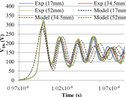
The measured VDS turn-off waveforms for each of the
samples and for each of the 5 designs modelled are shown in Fig. 18 and a summary of the trends observed in Fig. 19. The frequency shift with increasing dx can clearly be seen in both but the increase in peak voltage with dx is less clear. It is difficult to accurately measure the difference in peak voltage with an oscilloscope because of limited resolution and because other lower frequency oscillations in the circuit or
measurement equipment can affect the measurement amplitude.
Since the amplitude measurements cannot be relied upon, the oscillation frequency measurements are used for comparison. The model predicts a shift in oscillation frequency of 4.2MHz between dx=17mm and dx=52mm, which corresponds to a 20V increase in the peak VDS. In the experimental
measurements, the mean frequency shift was 1.6MHz and a peak shift between any two of these designs of 2.5Mhz. The model estimates the effective commutation loop inductance at 40.1nH for dx = 17mm and 48.5nH for dx = 52mm. If these modelled inductance values are taken with the maximum measured oscillation frequency at dx = 17mm (49.6MHz) an estimated MOSFET output capacitance of 0.256nF is obtained, and the minimum observed frequency at dx = 54mm (47.1MHz) gives an estimated MOSFET output capacitance of 0.236nF. The fact that these observed capacitance values are not consistent suggests there must be some error in the inductance estimations in the PEEC model. If the relative change in parasitic inductance predicted by the PEEC model between the two extremes of dx (8.4nH) can be assumed to be approximately correct, there must be errors in both the absolute PEEC predicted inductance values and the 0.29nF value used for the MOSFET output capacitance CM.
The linear model for this component is one source of error in CM.
It is obvious that more work is required to integrate better device and electrical parasitic models to enable useful, quantitative device switching waveform predictions.
C. Thermal Results
[image:10.595.318.533.85.245.2]The peak temperature recorded at the MOSFET and diode during simulation of each of the 5 designs is shown in Fig. 20 along with the peak recorded temperature. There were some small variations (1-2°C) in ambient temperature over the course of the experimental testing and so the recorded temperatures have been adjusted so that the temperature at the start of each test is 29°C to allow comparison with a single simulation.
[image:10.595.57.261.93.250.2]TPEL-Reg-2014-10-1702.R1
The measured MOSFET temperatures follow a linear trend with the exception of one sample with dx=52mm, which appears to have a particularly poor solder layer under the MOSFET and the peak temperature is higher than expected. The peak MOSFET temperature predictions are a close match for the experimental measurement, with a consistent error of around 1°C, therefore the simulation could be used to accurately differentiate between the designs in terms of peak MOSFET temperature. Since its self-thermal impedance does not change, the MOSFET temperature variation is determined by changes in the coupled thermal impedance with the diode, and this effect is significant as the mean diode power dissipation (8.67W) is approximately double the mean MOSFET power dissipation (4.75W).
There is a greater spread in the diode temperature measurements at each design point. This is because the diode’s temperature is dominated by its larger self-heating power and small changes in the thickness and void density of the solder layer beneath the device can have a noticeable effect on the temperature rise. The temperatures recorded for the centered diode, where dx = 34.5mm, are also consistently higher than the predicted trend. This is likely to be because the IMS substrate was clamped to the heat-sink with 8 bolts
around its periphery which results in a lower interface pressure, and therefore increased interface thermal resistance, in the center. The opposite effect is seen in the simulation results, as theoretically the diode will have lower self-thermal impedance when it is positioned in the center of the design. Despite these differences, both simulation and experimental results predict a general decreasing trend in peak temperature. Improved models of the sink and particularly the heat-sink-substrate interface would be required to exactly reproduce the trends seen in the diode measurements.
The high frequency dynamics of the thermal model are illustrated in Fig. 21 where the model waveforms for dx=17mm along with the waveforms taken from the samples which exhibited the minimum and maximum temperatures for this value of dx.
D. Thermal Start-up Transient
[image:11.595.62.271.98.258.2] [image:11.595.309.530.456.736.2]Using the mean power dissipation at each device, available from the operating point simulation, a longer term, thermal only, start-up simulation was performed. The heat sources in the physical thermal model were driven by DC sources in the behavioral model and the parasitic model was disabled. Simulations of the first 1000 seconds with over 800 time-steps were performed and took a total of 3 minutes 30 seconds including MOR for all 5 designs. Surface temperature plots were generated at a number of time-steps, taking advantage of the MOR 3D post-processing capabilities and these are compared with corresponding IR images in Fig. 22. Note that surface or arbitrary cross-sectional plane plots for heat-flux or temperature (and current density or voltage for the previous operating point example where the parasitic model is enabled) Fig. 20 – Predicted and Measured Variations in Thermal Performance
Fig. 21 – High frequency temperature ripple for model and minimum and
[image:11.595.50.275.565.710.2]TPEL-Reg-2014-10-1702.R1
can be generated at any time-step from the reduced order model results with no further simulation. Agreement between the experimental and simulated low frequency thermal response is excellent across the entire design. Some small differences in the IMS substrate tile temperature distribution are seen which are due to inaccuracies in the substrate-heat-sink interface model and the temperature distribution across the semiconductors differs due to inconsistencies in the die-attach solder, which are not modelled.
V. LIMITATIONS OF THE APPROACH
The approach outlined has the potential to allow rapid multidisciplinary simulations that could enable virtual prototyping in power electronics, however for the approach to be applicable to more complex systems, such as complete power converters, there are a number of limitations which must be addressed.
Both the thermal and parasitic models must be linear due to the model order reduction techniques, MOR techniques compatible with non-linear systems are required to overcome this limitation which are not so well developed.
The parasitic model only considers inductive parasitics, not capacitive parasitics, however both the PEEC method and MOR techniques can be modified to account for capacitive parasitics.
Coupling between the thermal and electrical geometrical models is limited to a small number of model inputs and outputs, if a high level of distributed coupling is required (such as mapping current distribution to heat generation) a large number of model inputs and outputs is required which can reduce the effectiveness of the MOR approach.
The parasitic model assumes homogeneous relative permeability which does not allow modelling of magnetic cores. Work by ETH has shown that the PEEC method can be modified to overcome this using a hybrid PEEC-BEM approach [4, 33] but MOR techniques compatible with this modified PEEC need to be validated.
The time taken to solve the dense equations that result from the PEEC method, and hence generate a reduced order model, has a cubic dependency on the number of equations in the original model. This limits the allowable complexity of the parasitic model. More advanced solvers such as those suggested in [30-32] are needed to resolve this issue and this is an ongoing area of research.
The semiconductor device models use simple switch models and linear components which cannot accurately predict switching waveforms. Better models are required, and the ability to import existing models in SPICE format or to have models that can be easily parameterised from datasheet information is desirable.
Thermal boundary conditions must be specified manually in terms of heat-transfer coefficients, effects such as fluid flow in thermal management systems cannot be modelled. In a rapid prototyping tool, full CFD simulations will not be suitable but a method for automatically determining boundary conditions for common heat-sink geometries is needed.
The general 3D modelling capabilities are significantly lower than those in commercial FEA type simulation packages, for example the ability to model curved or complicated shapes or import from CAD packages. For a design tool, a trade-off between advanced modelling capabilities and speed, simplicity and ease of use must be found.
VI. CONCLUSIONS ANDFUTUREWORK
This work has demonstrated a virtual design and optimization tool structure using model order reduction (MOR) techniques to produce power-electronics specific design tools for rapid virtual prototyping of power electronic systems. This work has demonstrated that the techniques can provide a rapid qualitative or semi-quantitative comparison between potential designs, and has identified areas where improvements must be made to enable higher performance virtual prototyping tools for power electronics. Future work will aim to address the limitations identified and extend the capabilities of the design tool. Further areas of particular interest are: the ability to use the rapid thermal simulations to enable “design for reliability” through addition of reliability post-processing using empirical models[34] and cycle-counting methods[35], the improvement of design functionality aspects such as design scripting capabilities and integration of suitable optimization algorithms.
REFERENCES
[1] D. Cottet, S. Hartmann, and U. Schlapbach, "Numerical Simulations for Electromagnetic Power Module Design," in Power Semiconductor Devices and IC's, 2006. ISPSD 2006. IEEE International Symposium on, 2006, pp. 1-4.
[2] R. Azar, F. Udrea, W. T. Ng, F. Dawson, W. Findlay, and P. Waind, "The Current Sharing Optimization of Paralleled IGBTs in a Power Module Tile Using a PSpice Frequency Dependent Impedance Model," IEEE Transactions on Power Electronics, vol. 23, pp. 206-217, Jan 2008.
[3] A. Musing, M. L. Heldwein, T. Friedli, and J. W. Kolar, "Steps Towards Prediction of Conducted Emission Levels of an RB-IGBT Indirect Matrix Converter," inPCC '07, Nagoya, 2007, pp. 1181-1188.
[4] I. F. Kovacevic, T. Friedli, A. M. Musing, and J. W. Kolar, "3-D Electromagnetic Modeling of Parasitics and Mutual Coupling in EMI Filters,"Power Electronics, IEEE Transactions on,vol. 29, pp. 135-149, 2014.
[5] A. Castellazzi, M. Ciappa, W. Fichtner, G. Lourdel, and M. Mermet-Guyennet, "Compact Modelling and analysis of power sharing unbalances in IGBT modules used in traction applications," Microelectronics Reliability,vol. 46, pp. 1754-1759, 2006.
[6] S.-L. Lee, W. G. Odendaal, and J. D. van Wyk, "Thermo-Mechanical Stress Analysis for an Integrated Passive Resonant Module," IEEE Transactions on Industry Applications, vol. 40, pp. 94-102, January/February 2004 2004.
[7] U. Drofenik, I. Kovacevic, R. Schmidt, and J. W. Kolar, "Multi-domain simulation of transient junction temperatures and resulting stress-strain behavior of power switches for long-term mission profiles," inControl and Modeling for Power Electronics, 2008. COMPEL 2008. 11th Workshop on, 2008, pp. 1-7.
[8] D. Cottet, "Industry perspective on multi domain simulations and virtual prototyping," in Control and Modeling for Power Electronics, 2008. COMPEL 2008. 11th Workshop on, 2008, pp. 1-6.
TPEL-Reg-2014-10-1702.R1
[10] P. Solomalala, J. Saiz, A. Lafosse, M. Mermet-Guyennet, A. Castellazzi, X. Chauffieur, et al., "Multi-domain simulation platform for virtual prototyping of integrated power systems," in Power Electronics and Applications, 2007 European Conference on, 2007, pp. 1-10.
[11] W. Rui, F. Iannuzzo, W. Huai, and F. Blaabjerg, "Fast and accurate Icepak-PSpice co-simulation of IGBTs under short-circuit with an advanced PSpice model," inPower Electronics, Machines and Drives (PEMD 2014), 7th IET International Conference on, 2014, pp. 1-5. [12] R. Chen, F. Canales, B. Yang, and J. D. van Wyk, "Volumetric Optimal
Design of Passive Integrated Power Electronics Module (IPEM) for Distributed Power System (DPS) Front-End DC/DC Converter," IEEE Transactions on Industry Applications, vol. 41, pp. 9-17, January/February 2005.
[13] M. Musallam and C. M. Johnson, "Real-Time Compact Thermal Models for Health Management of Power Electronics,"Power Electronics, IEEE Transactions on,vol. 25, pp. 1416-1425, 2010.
[14] P. L. Evans, A. Castellazzi, and C. M. Johnson, "Automated Fast Extraction of Compact Thermal Models for Power Electronic Modules," Power Electronics, IEEE Transactions on,vol. 28, pp. 4791-4802, 2013. [15] M. Kamon, M. J. Tsuk, and J. K. White, "FASTHENRY: a multipole-accelerated 3-D inductance extraction program,"IEEE Transactions on Microwave Theory and Techniques,vol. 42, pp. 1750-1758, Sept 1994. [16] U. Drofenik, D. Cottet, A. Musing, J.-M. Meyer, and J. W. Kolar,
"Computationally Efficient Integration of Complex Thermal Multi-Chip Power Module Models into Circuit Simulators," inPCC '07, Nagoya, Japan, 2007, pp. 550-557.
[17] J. Biela, J. W. Kolar, A. Stupar, U. Drofenik, and A. Muesing, "Towards Virtual Prototyping and Comprehensive Multi-Objective Optimisation in Power Electronics," presented at the PCIM 2010, Nuremberg, Germany, 2010.
[18] Gecko Research. Available: http://www.gecko-research.com/
[19] E. Rudnyi and J. Korvink, "Model Order Reduction for Large Scale Engineering Models Developed in ANSYS," in Applied Parallel Computing. State of the Art in Scientific Computing. vol. 3732, J.
Dongarra, K. Madsen, and J. Waśniewski, Eds., ed: Springer Berlin
Heidelberg, 2006, pp. 349-356.
[20] P. L. Evans, A. Castellazzi, S. Bozhko, and C. M. Johnson, "Automatic Design Optimisation for Power Electronics Modules Based on Rapid Dynamic Thermal Analysis," in Power Electronics and Applications (EPE 20113), Proceedings of the 2013-15th European Conference on., 2013.
[21] Y. Saad,Numerical methods for large eigenvalue problems. Manchester, UK: Manchester University Press, 1992.
[22] R. W. Freund, "Krylov-subspace methods for reduced-order modeling in circuit simulation,"Journal of Computational and Applied Mathematics, vol. 123, pp. 395-421, 2000.
[23] T. Bechtold, E. B. Rudnyi, and J. G. Korvink, Fast Simulation of Electro-Thermal MEMs. Freiburg: Springer, 2006.
[24] T. Bechtold, E. B. Rudnyi, and J. G. Korvink, "Error indicators for fully automatic extraction of heat-transfer macromodels for MEMS,"Journal of Micromechanics and Microengineering,vol. 15, p. 430, 2005. [25] T. A. Davis and E. P. Natarajan, "Algorithm 907: KLU, a direct sparse
solver for circuit simulation problems," ACM Transactions on Mathematical Software,vol. 37, 2010.
[26] A. E. Ruehli, "Inductance Calculations in a Complex Integrated Circuit Environment,"IBM Journal of Research and Development,vol. 16, pp. 470-481, 1972.
[27] M. Celik, L. T. Pileggi, and A. A.,IC interconnect analysis: Kluwer Academic Publishers, 2002.
[28] S. Tan and L. He.,Advanced Model Order Reduction Techniques in VLSI Design: Cambridge University Press, 2007.
[29] A. Odabasioglu, M. Celik, and L. T. Pileggi, "PRIMA: passive reduced-order interconnect macromodeling algorithm,"Computer-Aided Design of Integrated Circuits and Systems, IEEE Transactions on,vol. 17, pp. 645-654, 1998.
[30] G. Antonini, "Fast multipole method for time domain PEEC analysis," Mobile Computing, IEEE Transactions on,vol. 2, pp. 275-287, 2003. [31] D. Gope, A. E. Ruehli, and V. Jandhyala, "Speeding Up PEEC Partial
Inductance Computations Using a QR-Based Algorithm," Very Large Scale Integration (VLSI) Systems, IEEE Transactions on,vol. 15, pp. 60-68, 2007.
[32] D. Romano and G. Antonini, "Partitioned Model Order Reduction of Partial Element Equivalent Circuit Models," Components, Packaging and Manufacturing Technology, IEEE Transactions on,vol. 4, pp. 1503-1514, 2014.
[33] I. F. Kovacevic, A. M. Musing, and J. W. Kolar, "An Extension of PEEC Method for Magnetic Materials Modeling in Frequency Domain," Magnetics, IEEE Transactions on,vol. 47, pp. 910-913.
[34] L. Yang, P. Agyakwa, and C. M. Johnson, "A Time-Domain Physics-Of-Failure Model For The Lifetime Prediction Of Wire Bond Interconnects, Microelectronics Reliability,"Microelectronics Reliability, vol. 51, pp. 1882-1886, 2011.